JP5673075B2 - Tunable interference filter, optical module, and optical analyzer - Google Patents
Tunable interference filter, optical module, and optical analyzer Download PDFInfo
- Publication number
- JP5673075B2 JP5673075B2 JP2010284574A JP2010284574A JP5673075B2 JP 5673075 B2 JP5673075 B2 JP 5673075B2 JP 2010284574 A JP2010284574 A JP 2010284574A JP 2010284574 A JP2010284574 A JP 2010284574A JP 5673075 B2 JP5673075 B2 JP 5673075B2
- Authority
- JP
- Japan
- Prior art keywords
- electrode
- substrate
- partial
- movable
- fixed
- Prior art date
- Legal status (The legal status is an assumption and is not a legal conclusion. Google has not performed a legal analysis and makes no representation as to the accuracy of the status listed.)
- Expired - Fee Related
Links
Images


Description
本発明は、特定波長の光を取得する波長可変干渉フィルター、光モジュール、および光分析装置に関する。 The present invention relates to a tunable interference filter, an optical module, and an optical analyzer that acquire light of a specific wavelength.
従来、複数波長の光から、特定波長の光を取り出す波長可変干渉フィルター(光フィルター素子)が知られている(例えば、特許文献1参照)。 Conventionally, a wavelength variable interference filter (optical filter element) that extracts light of a specific wavelength from light of a plurality of wavelengths is known (see, for example, Patent Document 1).
この特許文献1に記載の波長可変干渉フィルター(光学フィルタ装置)は、可動部(第1部分)、および可動部を支持するダイヤフラム(第2部分)を備えた第1基板と、第1基板に対向する第2基板とを備えている。また、第1基板の可動部には、可動ミラーが形成され、第2基板の可動部に対向する面には、固定ミラーが形成されている。そして、第1基板および第2基板には、それぞれリング状の電極が設けられ、静電アクチュエーターが構成されている。このような波長可変干渉フィルターでは、電極間に電圧を印加することで、静電引力によりダイヤフラムを撓ませて、固定ミラーおよび可動ミラーの間のギャップを変動させることができ、所望波長の光を取り出すことができる。 The tunable interference filter (optical filter device) described in Patent Document 1 includes a movable substrate (first portion), a first substrate including a diaphragm (second portion) that supports the movable portion, and a first substrate. And an opposing second substrate. In addition, a movable mirror is formed on the movable part of the first substrate, and a fixed mirror is formed on the surface facing the movable part of the second substrate. Each of the first substrate and the second substrate is provided with a ring-shaped electrode, thereby forming an electrostatic actuator. In such a wavelength tunable interference filter, by applying a voltage between the electrodes, the diaphragm can be deflected by electrostatic attraction, and the gap between the fixed mirror and the movable mirror can be changed, and light of a desired wavelength can be changed. It can be taken out.
また、静電アクチュエーターを複数の部分アクチュエーターをそれぞれ制御可能な波長可変干渉フィルターも知られている(例えば特許文献2)。 There is also known a variable wavelength interference filter capable of controlling an electrostatic actuator and a plurality of partial actuators (for example, Patent Document 2).
この特許文献2の波長可変干渉フィルター(波長可変フィルタ)は、導電性の可動部を有する第1の基板と、第2の基板とを備え、第1の基板の可動部と、第2の基板の可動部に対向する位置とにそれぞれ反射膜が設けられている。そして、これらの第2の基板の可動部に対向する位置には、円弧状の2つの駆動電極を設けられている。このような波長可変干渉フィルターでは、2つの駆動電極のそれぞれに異なる電極を印加することで、各駆動電極と可動部との間に、それぞれ異なる静電引力を作用させることが可能となる。
The wavelength tunable interference filter (wavelength tunable filter) of
ところで、上記特許文献1に記載の波長可変干渉フィルターにおいて、第1基板に設けられた電極と第2基板に設けられた電極との間の電極間ギャップが均一である場合、これらの電極間に電圧を印加すると、ダイヤフラムが均一に撓む。したがって、可動部は、姿勢を維持した状態で、第2基板側に移動する。しかしながら、ダイヤフラムに僅かな傾斜があり、電極間ギャップが不均一である場合では、電極間ギャップが小さいほど大きな静電引力が作用するため、ダイヤフラムの傾斜が大きくなる。つまり、初期状態において、ダイヤフラムの傾斜が分光精度に影響を与えない許容値以内のものであっても、電極間に電圧を印加した状態では、ダイヤフラムの傾斜が大きくなり、分光精度が悪化してしまう場合がある。 By the way, in the wavelength tunable interference filter described in Patent Document 1, when the interelectrode gap between the electrode provided on the first substrate and the electrode provided on the second substrate is uniform, between these electrodes. When a voltage is applied, the diaphragm bends uniformly. Therefore, the movable part moves to the second substrate side while maintaining the posture. However, when the diaphragm has a slight inclination and the gap between the electrodes is not uniform, the smaller the gap between the electrodes, the larger the electrostatic attractive force acts, so that the inclination of the diaphragm increases. That is, in the initial state, even if the tilt of the diaphragm is within an allowable value that does not affect the spectral accuracy, the tilt of the diaphragm increases and the spectral accuracy deteriorates when a voltage is applied between the electrodes. May end up.
一方、特許文献2では、静電アクチュエーターを構成する駆動電極を2つ以上に分割されている。このため、これらの駆動電極に印加する電圧を制御することで、ダイヤフラムの傾斜が大きくなった場合でも、それを補正することもできる。しかしながら、この場合、ダイヤフラムの傾斜状態を判別して、それに応じた電圧を各駆動電極に与える必要がある。したがって、ダイヤフラムの傾斜状態や、電極間ギャップを測定するためのセンサーを設ける必要があるなど、構成が複雑化するという問題がある。また、測定したダイヤフラムの傾斜状態や電極間ギャップから、各駆動電圧に印加するための駆動電圧を算出する必要があり、静電アクチュエーターの駆動制御が複雑化するという問題もある。
On the other hand, in
本発明は上述のような問題に鑑みて、簡単な構成で、反射膜間のギャップ寸法を変化させた場合でも分解能の低下を抑制できる波長可変干渉フィルター、光モジュール、および光分析装置を提供することを目的とする。 In view of the above problems, the present invention provides a variable wavelength interference filter, an optical module, and an optical analyzer that can suppress a decrease in resolution even when the gap size between reflecting films is changed with a simple configuration. For the purpose.
本発明の波長可変干渉フィルターは、第一基板と、前記第一基板に対向する第二基板と、前記第一基板に設けられた第一反射膜と、前記第二基板に設けられ、前記第一反射膜とギャップを介して対向する第二反射膜と、前記第一基板に設けられた第一電極、および前記第二基板に設けられて前記第一電極に対向する第二電極を備えた静電アクチュエーターと、を具備し、前記第一電極は、前記第一基板および前記第二基板を基板厚み方向から見た平面視において、それぞれ同一面積となる形状に形成され、前記第一反射膜の中心点を中心とした仮想円上で、周方向に沿って等角度間隔で配置された複数の第一部分電極を備え、前記第二電極は、前記平面視において、前記第一部分電極と同一形状に形成され、かつ、前記第一部分電極と重なる位置に設けられた複数の第二部分電極を備え、前記静電アクチュエーターは、互いに対向する前記第一部分電極および前記第二部分電極により構成された部分アクチュエーターを3つ以上備えるとともに、前記3つ以上の部分アクチュエーターのうちのいずれか2つにより電圧印加用部分アクチュエーターが構成され、2つの前記電圧印加用部分アクチュエーター間で、前記3つ以上の部分アクチュエーターが電気的に直列に接続されていることを特徴とする。
また、本発明の波長可変干渉フィルターは、第一基板と、前記第一基板に対向する第二基板と、前記第一基板に設けられた第一反射膜と、前記第二基板に設けられ、前記第一反射膜とギャップを介して対向する第二反射膜と、前記第一基板に設けられた第一電極と前記第二基板に設けられた第二電極とが対向する第一容量部と、前記第一基板に設けられた第三電極と前記第二基板に設けられた第四電極とが対向する第二容量部と、前記第一基板に設けられた第五電極と前記第二基板に設けられた第六電極とが対向する第三容量部と、を有する静電アクチュエーターと、を備え、前記第一電極、前記第二電極、前記第三電極、前記第四電極、前記第五電極および前記第六電極の面積は同一であり、前記第一容量部と前記第二容量部と前記第三容量部とは、前記第一基板および前記第二基板を基板厚み方向から見た平面視において、前記第一反射膜の中心点を中心とした仮想円上で、周方向に沿って等角度間隔で配置され、かつ、電気的に直列に接続されていることを特徴とする。
The wavelength tunable interference filter of the present invention includes a first substrate, a second substrate facing the first substrate, a first reflective film provided on the first substrate, and provided on the second substrate. A second reflective film facing the reflective film through a gap; a first electrode provided on the first substrate; and a second electrode provided on the second substrate and facing the first electrode. An electrostatic actuator, wherein the first electrode is formed in a shape having the same area in a plan view of the first substrate and the second substrate viewed from the substrate thickness direction , and the first reflective film A plurality of first partial electrodes arranged at equiangular intervals along the circumferential direction on a virtual circle centered on the center point of the second electrode, the second electrode having the same shape as the first partial electrode in the plan view And overlaps the first partial electrode Comprising a plurality of second sub-electrodes provided on the location, the electrostatic actuator, as well as obtain Bei three or more configured partial actuators by the first partial electrode and the second partial electrodes facing each other, the three Any two of the above partial actuators constitute a voltage application partial actuator, and the three or more partial actuators are electrically connected in series between the two voltage application partial actuators . It is characterized by.
Further, the wavelength tunable interference filter of the present invention is provided on the first substrate, the second substrate facing the first substrate, the first reflective film provided on the first substrate, and the second substrate, A second reflective film opposed to the first reflective film via a gap; a first electrode provided on the first substrate; and a first capacitor portion opposed to the second electrode provided on the second substrate; , A second capacitor portion facing a third electrode provided on the first substrate and a fourth electrode provided on the second substrate, a fifth electrode provided on the first substrate, and the second substrate An electrostatic actuator having a third capacitor portion facing a sixth electrode provided on the first electrode, the second electrode, the third electrode, the fourth electrode, and the fifth electrode The areas of the electrode and the sixth electrode are the same, and the first capacitor portion, the second capacitor portion, and the third capacitor The part is an imaginary circle centered on the center point of the first reflective film at an equal angular interval along the circumferential direction in a plan view of the first substrate and the second substrate viewed from the substrate thickness direction. It is arrange | positioned and is electrically connected in series, It is characterized by the above-mentioned.
ここで、複数の部分アクチュエーターが電気的に直列に接続されるとは、第一電極同士の接続、第二電極同士の接続が交互に繰り返されて接続される構成を指すものである。例えば、第1〜第4部分アクチュエーターの4つの部分アクチュエーターが、この順で電気的に直列接続される場合では、第1部分アクチュエーターの第一電極と第2部分アクチュエーターの第一電極とが接続され、第2部分アクチュエーターの第二電極と第3部分アクチュエーターの第二電極とが接続され、第3部分アクチュエーターの第一電極と第4部分アクチュエーターの第一電極とが接続される。 Here, the phrase “the plurality of partial actuators are electrically connected in series” refers to a configuration in which the connection between the first electrodes and the connection between the second electrodes are alternately repeated. For example, when four partial actuators of the first to fourth partial actuators are electrically connected in series in this order, the first electrode of the first partial actuator and the first electrode of the second partial actuator are connected. The second electrode of the second partial actuator and the second electrode of the third partial actuator are connected, and the first electrode of the third partial actuator and the first electrode of the fourth partial actuator are connected .
一般に静電アクチュエーターで発生する静電引力Fは、その静電アクチュエーターにより保持される電荷量と電極の面積とに基づいて変化する。また、この電荷量は、電極の面積が増大するに従って、また、電極間の距離が小さくなるに従って増大する。
これに対し、本発明では、部分アクチュエーターが、電気的に直列に接続されているので、2つの電圧印加用部分アクチュエーター間で電圧Vを印加すると、それぞれ容量リアクタンスに応じた分圧が印加されることとなり、各部分アクチュエーターにおいて保持される電荷量は同一となる。また、各第一部分電極が平面視において同一面積を有し、各第二部分電極は、第一部分電極と同一の形状に形成されている。このため、各部分アクチュエーターで作用する静電引力は、電極の面積、および保持される電荷量が同値となるため、同一の大きさとなる。
したがって、本発明では、第一基板または第二基板の傾斜により、各部分アクチュエーターにおける部分電極ギャップに差があった場合でも、各部分アクチュエーターに同じ大きさの静電引力を作用させることができる。これにより、第一反射膜および第二反射膜の間のギャップを変更した際に、第一基板または第二基板の一部に大きい静電引力が作用して第一および第二反射膜の平行関係を維持できなくなる不都合を防止でき、分解能の低下を抑えることができる。
Generally, the electrostatic attractive force F generated by an electrostatic actuator changes based on the amount of charge held by the electrostatic actuator and the area of the electrode. The amount of charge increases as the area of the electrode increases and as the distance between the electrodes decreases.
On the other hand, in the present invention, since the partial actuators are electrically connected in series, when a voltage V is applied between the two voltage application partial actuators, a partial pressure corresponding to each capacitive reactance is applied. That is, the amount of charge held in each partial actuator is the same. Moreover, each 1st partial electrode has the same area in planar view, and each 2nd partial electrode is formed in the same shape as a 1st partial electrode. For this reason, the electrostatic attraction acting on each partial actuator has the same value because the area of the electrode and the amount of charge held are the same.
Therefore, in the present invention, even when there is a difference in the partial electrode gap in each partial actuator due to the inclination of the first substrate or the second substrate, it is possible to apply the same electrostatic attraction force to each partial actuator. Thereby, when the gap between the first reflective film and the second reflective film is changed, a large electrostatic attraction acts on a part of the first substrate or the second substrate, and the first and second reflective films are parallel to each other. The inconvenience that the relationship cannot be maintained can be prevented, and the decrease in resolution can be suppressed.
本発明の波長可変干渉フィルターは、前記複数の第一部分電極は、前記平面視において、前記第一反射膜の中心点を中心とした仮想円上で、周方向に沿って等角度間隔で配置され、前記複数の部分アクチュエーターのうちのいずれか2つにより電圧印加用部分アクチュエーターが構成され、前記静電アクチュエーターにおいて、2つの前記電圧印加用部分アクチュエーター間で、前記複数の部分アクチュエーターが電気的に直列に接続されていることが好ましい。
本発明では、2つの電圧印加用部分アクチュエーター間に駆動電圧を印加するだけで、上述のように、各部分アクチュエーターに作用させる静電引力を均一にすることができ、分解能の低下を抑えることができる。このため、各部分アクチュエーターに印加する電圧を制御するための複雑な回路を不要にでき、各部分アクチュエーターに対する個別の電圧制御をも行う必要がないので、静電アクチュエーターの制御も容易に実施できる。
なお、部分アクチュエーターが2つである場合は、これらの2つの部分アクチュエーターが電圧印加用部分アクチュエーターであり、2つの電圧印加用部分アクチュエーターが直列に接続される構成となる。
In the wavelength tunable interference filter according to the aspect of the invention, the plurality of first partial electrodes are arranged at equiangular intervals along the circumferential direction on a virtual circle centered on the center point of the first reflective film in the plan view. A voltage applying partial actuator is configured by any two of the plurality of partial actuators, and in the electrostatic actuator, the plurality of partial actuators are electrically connected in series between the two voltage applying partial actuators. It is preferable that it is connected to.
In the present invention, as described above, the electrostatic attractive force acting on each partial actuator can be made uniform by simply applying a drive voltage between the two voltage application partial actuators, and the reduction in resolution can be suppressed. it can. For this reason, a complicated circuit for controlling the voltage applied to each partial actuator can be eliminated, and it is not necessary to perform individual voltage control for each partial actuator. Therefore, the electrostatic actuator can be easily controlled.
When there are two partial actuators, these two partial actuators are voltage application partial actuators, and the two voltage application partial actuators are connected in series.
本発明の波長可変干渉フィルターでは、2つの前記電圧印加用部分アクチュエーターは、前記仮想円上で、互いに隣り合って配置され、前記静電アクチュエーターにおいて、2つの前記電圧印加用部分アクチュエーター間で、前記仮想円の周方向に沿って配列された前記部分アクチュエーターが順に電気的に直列に接続されたことが好ましい。 In the wavelength tunable interference filter of the present invention, the two voltage application partial actuators are arranged adjacent to each other on the virtual circle, and in the electrostatic actuator, between the two voltage application partial actuators, It is preferable that the partial actuators arranged along the circumferential direction of the virtual circle are sequentially electrically connected in series.
この発明では、部分アクチュエーターは、仮想円の円周方向に並ぶ順に直列に接続されている。このような構成であれば、各部分アクチュエーター間を接続する接続電極部を短くすることができ、抵抗を低減させることができる。 In the present invention, the partial actuators are connected in series in the order in which they are arranged in the circumferential direction of the virtual circle. With such a configuration, it is possible to shorten the connection electrode portion that connects the partial actuators, and to reduce the resistance.
本発明の波長可変干渉フィルターでは、前記静電アクチュエーターが複数設けられ、これらの静電アクチュエーターが電気的に並列に接続されたことが好ましい。 In the wavelength tunable interference filter of the present invention, it is preferable that a plurality of the electrostatic actuators are provided and these electrostatic actuators are electrically connected in parallel.
この発明では、上述のように、部分アクチュエーターが等角度間隔で配置されていた静電アクチュエーターが複数設けられている。上述したように、各部分アクチュエーターには分圧された電圧が印加されるため、1つの静電アクチュエーターを構成する部分アクチュエーターの数が多ければ、各部分アクチュエーターに印加される分圧値が小さくなる。この場合、部分アクチュエーターで作用する静電引力も小さくなってしまい、所望の静電引力を得るために、駆動電圧を大きくする必要がある。これに対して、本発明では、上述のような静電アクチュエーターを並列接続にすることで、小さい駆動電圧で所望の静電引力を得ることができる。
例えば、2つの部分アクチュエーターにより構成された静電アクチュエーターを2つ並列接続する波長可変干渉フィルターと、4つの部分アクチュエーターにより構成された1つの静電アクチュエーターとを比較した場合、前者の波長可変干渉フィルターは、後者の波長可変干渉フィルターの略半分の駆動電圧で、後者の波長可変干渉フィルターと同じ静電引力を得ることができる。
In the present invention, as described above, a plurality of electrostatic actuators in which the partial actuators are arranged at equiangular intervals are provided. As described above, since a divided voltage is applied to each partial actuator, if the number of partial actuators constituting one electrostatic actuator is large, the partial pressure value applied to each partial actuator becomes small. . In this case, the electrostatic attractive force acting on the partial actuator is also reduced, and it is necessary to increase the drive voltage in order to obtain a desired electrostatic attractive force. On the other hand, in the present invention, a desired electrostatic attraction can be obtained with a small driving voltage by connecting the above-described electrostatic actuators in parallel.
For example, when comparing a tunable interference filter in which two electrostatic actuators composed of two partial actuators are connected in parallel with a single electrostatic actuator composed of four partial actuators, the former tunable interference filter Can obtain the same electrostatic attraction as the latter wavelength tunable interference filter with a driving voltage almost half that of the latter wavelength tunable interference filter.
本発明の光モジュールは、上述したような波長可変干渉フィルターと、前記波長可変干渉フィルターにより取り出された光を検出する検出部と、を具備したことを特徴とする。 An optical module according to the present invention includes the above-described variable wavelength interference filter and a detection unit that detects light extracted by the variable wavelength interference filter.
この発明では、光モジュールは、上述したような波長可変干渉フィルターを備えている。波長可変干渉フィルターは、上記のように、第一反射膜および第二反射膜の間のギャップを変更した場合でも、各部分アクチュエーターに同一の大きさの静電引力を作用させることができ、分解能の低下を抑えることができる。
したがって、このような波長可変干渉フィルターを備えた光モジュールでは、高分解能で取り出された光を検出部で検出することができるので、高精度な検出結果を得ることができる。
In the present invention, the optical module includes the wavelength variable interference filter as described above. As described above, the variable wavelength interference filter can apply the same electrostatic attraction force to each partial actuator even when the gap between the first reflective film and the second reflective film is changed. Can be suppressed.
Therefore, in the optical module provided with such a variable wavelength interference filter, the light extracted with high resolution can be detected by the detection unit, so that a highly accurate detection result can be obtained.
本発明の光分析装置は、上述したような光モジュールと、前記光モジュールの前記検出部により検出された光に基づいて、前記光の光特性を分析する分析処理部と、を具備したことを特徴とする。 The optical analyzer of the present invention includes the optical module as described above, and an analysis processing unit that analyzes the optical characteristics of the light based on the light detected by the detection unit of the optical module. Features.
ここで、光分析装置としては、上記のような光モジュールから出力される電気信号に基づいて、光モジュールに入射した光の色度や明るさなどを分析する光測定器、ガスの吸収波長を検出してガスの種類を検査するガス検出装置、受光した光からその波長の光に含まれるデータを取得する光通信装置などを例示することができる。
この発明では、光分析装置は、上述したような光モジュールを備えている。光モジュールは、上記のように、高分解能で取り出された光を検出して、高精度な検出結果を得ることができる。したがって、このような光モジュールを備えた光分析装置では、高精度な検出結果に基づいて、正確な光分析処理を実施することができる。
Here, as an optical analyzer, based on the electrical signal output from the optical module as described above, an optical measuring device that analyzes the chromaticity and brightness of light incident on the optical module, the absorption wavelength of the gas Examples thereof include a gas detection device that detects the type of gas by detecting it, and an optical communication device that acquires data included in light of that wavelength from received light.
In the present invention, the optical analyzer includes the optical module as described above. As described above, the optical module can detect the light extracted with high resolution and obtain a highly accurate detection result. Therefore, in the optical analyzer equipped with such an optical module, an accurate optical analysis process can be performed based on a highly accurate detection result.
[第一実施形態]
以下、本発明に係る第一実施形態について、図面に基づいて説明する。
〔1.測色装置の全体構成〕
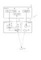
図1は、本発明に係る実施形態の測色装置(光分析装置)の概略構成を示す図である。
この測色装置1は、本発明の光分析装置であり、図1に示すように、検査対象Aに光を射出する光源装置2と、本発明の光モジュールである測色センサー3と、測色装置1の全体動作を制御する制御装置4とを備えている。そして、この測色装置1は、光源装置2から射出される光を検査対象Aにて反射させ、反射された検査対象光を測色センサー3にて受光し、測色センサー3から出力される検出信号に基づいて、検査対象光の色度、すなわち検査対象Aの色を分析して測定する装置である。
[First embodiment]
Hereinafter, a first embodiment according to the present invention will be described with reference to the drawings.
[1. Overall configuration of the color measuring device]
FIG. 1 is a diagram showing a schematic configuration of a color measurement device (light analysis device) according to an embodiment of the present invention.
The colorimetric device 1 is an optical analyzer according to the present invention. As shown in FIG. 1, a
〔2.光源装置の構成〕
光源装置2は、光源21、複数のレンズ22(図1には1つのみ記載)を備え、検査対象Aに対して白色光を射出する。複数のレンズ22には、コリメーターレンズが含まれていてもよく、この場合、光源装置2は、光源21から射出された白色光をコリメーターレンズにより平行光とし、図示しない投射レンズから検査対象Aに向かって射出する。
なお、本実施形態では、光源装置2を備える測色装置1を例示するが、例えば検査対象Aが液晶パネルなどの発光部材である場合、光源装置2が設けられない構成としてもよい。
[2. Configuration of light source device]
The
In the present embodiment, the colorimetric device 1 including the
〔3.測色センサーの構成〕
測色センサー3は、本発明の光モジュールを構成する。この測色センサー3は、図1に示すように、波長可変干渉フィルター5と、波長可変干渉フィルター5を透過した光を受光して検出する検出部31と、波長可変干渉フィルター5に駆動電圧を印加する電圧制御部32と、を備えている。また、測色センサー3は、波長可変干渉フィルター5に対向する位置に、検査対象Aで反射された反射光(検査対象光)を、内部に導光する図示しない入射光学レンズを備えている。そして、この測色センサー3は、波長可変干渉フィルター5により、入射光学レンズから入射した検査対象光のうち、所定波長の光のみを分光し、分光した光を検出部31にて受光する。
検出部31は、複数の光電交換素子により構成されており、受光量に応じた電気信号を生成する。そして、検出部31は、制御装置4に接続されており、生成した電気信号を受光信号として制御装置4に出力する。
[3. (Configuration of colorimetric sensor)
The
The
(3−1.波長可変干渉フィルターの構成)
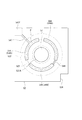
図2は、波長可変干渉フィルター5の概略構成を示す平面図であり、図3は、図2をIII−III線で断面した波長可変干渉フィルター5の断面図である。
波長可変干渉フィルター5は、図2に示すように、平面正方形状の板状の光学部材である。この波長可変干渉フィルター5は、図3に示すように、本発明の第一基板である固定基板51、および本発明の第二基板である可動基板52を備えている。これらの2枚の基板51,52は、それぞれ例えば、ソーダガラス、結晶性ガラス、石英ガラス、鉛ガラス、カリウムガラス、ホウケイ酸ガラス、無アルカリガラスなどの各種ガラスや、水晶などにより形成されている。そして、これらの2つの基板51,52は、外周部近傍に形成される接合部513,523が、例えば常温活性化接合やプラズマ重合膜を用いたシロキサン接合などにより、接合されることで、一体的に構成されている。
(3-1. Configuration of wavelength tunable interference filter)
FIG. 2 is a plan view showing a schematic configuration of the variable
As shown in FIG. 2, the wavelength
固定基板51には、本発明の第一反射膜を構成する固定反射膜56が設けられ、可動基板52には、本発明の第二反射膜を構成する可動反射膜57が設けられている。ここで、固定反射膜56は、固定基板51の可動基板52に対向する面に固定され、可動反射膜57は、可動基板52の固定基板51に対向する面に固定されている。また、これらの固定反射膜56および可動反射膜57は、ギャップを介して対向配置されている。
さらに、固定基板51と可動基板52との間には、固定反射膜56および可動反射膜57の間のギャップの寸法を調整するための静電アクチュエーター54が設けられている。この静電アクチュエーター54は、固定基板51側に設けられる本発明の第一電極としての固定電極541と、可動基板52側に設けられる本発明の第二電極としての可動電極542とを備えている。
The fixed
Further, an
(3−1−1.固定基板の構成)
図4は、第一実施形態の波長可変干渉フィルター5における固定基板51を可動基板52側から見た平面図である。
固定基板51は、厚みが例えば500μmに形成されるガラス基材を加工することで形成される。具体的には、図3に示すように、固定基板51には、エッチングにより電極形成溝511および反射膜固定部512が形成されている。この固定基板51は、可動基板52に対して厚み寸法が大きく形成されており、固定電極541および可動電極542間に電圧を印加した際の静電引力や、固定電極541の内部応力による固定基板51の撓みはない。
(3-1-1. Configuration of Fixed Substrate)
FIG. 4 is a plan view of the fixed
The fixed
電極形成溝511は、図4に示すように、平面視で、固定基板51の平面中心点を中心とした円形に形成されている。反射膜固定部512は、前記平面視において、電極形成溝511の中心部から可動基板52側に突出して形成される。
また、固定基板51には、電極形成溝511から、固定基板51の外周縁の頂点方向(例えば図4における左下方向、および右上方向)に向かって延出する一対の電極引出溝514(図示略)が設けられている。さらに、一対の電極引出溝のうちの一方の先端部(本実施形態では、図4において右上方向に延出した電極引出溝の先端部)には、図4に示すように、切欠部515が形成されている。
As shown in FIG. 4, the
Further, the fixed
そして、固定基板51の電極形成溝511の溝底部である電極形成面511Aには、固定電極541が形成されている。
この固定電極541は、図4に示すように、円弧状の複数の固定部分電極543(543A,543B,543C)により構成されている。これらの固定部分電極543は、本発明の第一部分電極を構成する。
これらの固定部分電極543A,543B,543Cは、それぞれ、基板厚み方向から見た平面視における平面形状が同一であり、かつ同一厚み寸法に形成されている。そして、これらの固定部分電極543A,543B,543Cは、平面視において、波長可変干渉フィルター5の平面中心を中心とした仮想円Pの円周に沿って、等角度間隔で配置されている。すなわち、これらの固定部分電極543A,543B,543Cは、各重心位置が120度間隔となるように、それぞれ配置されている。
A fixed
As shown in FIG. 4, the fixed
These fixed
ここで、3つの固定部分電極543のうち、固定部分電極543Aは、固定電極引出線545を備えている。この固定電極引出線545は、固定部分電極543Aの外周縁から、図4における左下方向に延出した電極引出溝514に沿って形成され、その先端部には、電圧制御部32に接続される電極パッド545Pが設けられている。
また、固定部分電極543Bと、固定部分電極543Cとは、固定電極接続線546により接続されている。
さらに、これらの固定部分電極543上には、固定電極541および可動電極542の間の放電を防止するための絶縁膜が積層されている。
Here, of the three fixed
The fixed
Further, an insulating film for preventing discharge between the fixed
反射膜固定部512は、上述したように、電極形成溝511と同軸上で、電極形成溝511よりも小さい径寸法となる円柱状に形成されている。なお、本実施形態では、図3に示すように、反射膜固定部512の可動基板52に対向する反射膜固定面512Aが、電極形成面511Aよりも可動基板52に近接して形成される例を示すが、これに限らない。電極形成面511Aおよび反射膜固定面512Aの高さ位置は、反射膜固定面512Aに固定される固定反射膜56、および可動基板52に形成される可動反射膜57の間のギャップの寸法、固定電極541および可動電極542の間の寸法、固定反射膜56や可動反射膜57の厚み寸法により適宜設定される。したがって、例えば、電極形成面511Aと反射膜固定面512Aとが同一面に形成される構成や、電極形成面511Aの中心部に、円柱凹溝上の反射膜固定溝が形成され、この反射膜固定溝の底面に反射膜固定面が形成される構成などとしてもよい。
As described above, the reflection
そして、反射膜固定面512Aには、円形状に形成される固定反射膜56が固定されている。この固定反射膜56としては、金属の単層膜により形成されるものであってもよく、誘電体多層膜により形成されるものであってもよく、さらには、誘電多層膜上にAg合金が形成される構成などとしてもよい。金属単層膜としては、例えばAg合金の単層膜を用いることができ、誘電体多層膜の場合は、例えば高屈折層をTiO2、低屈折層をSiO2とした誘電体多層膜を用いることができる。
A fixed
さらに、固定基板51は、可動基板52に対向する面とは反対側の面において、固定反射膜56に対応する位置に図示略の反射防止膜(AR)が形成されている。この反射防止膜は、低屈折率膜および高屈折率膜を交互に積層することで形成され、固定基板51の表面での可視光の反射率を低下させ、透過率を増大させる。
Further, the fixed
(3−1−2.可動基板の構成)
図5は、第一実施形態の波長可変干渉フィルター5における可動基板52を固定基板51側から見た平面図である。
可動基板52は、厚みが例えば200μmに形成されるガラス基材をエッチングにより加工することで形成される。
具体的には、可動基板52は、図2、図5に示すような平面視において、基板中心点を中心とした円形の可動部521と、可動部521と同軸であり可動部521を保持する保持部522と、を備えている。
また、可動基板52は、図2および図5に示すように、切欠部524を備えている。この切欠部524は、固定基板51の電極パッド545Pに対応する位置に設けられている。これにより、波長可変干渉フィルター5の可動基板52側から見た面に電極パッド545Pが露出する。
(3-1-2. Configuration of movable substrate)
FIG. 5 is a plan view of the
The
Specifically, the
In addition, the
可動部521は、保持部522よりも厚み寸法が大きく形成され、例えば、本実施形態では、可動基板52の厚み寸法と同一寸法である200μmに形成されている。また、可動部521は、反射膜固定部512に平行な可動面521Aを備え、この可動面521Aに、固定反射膜56とギャップを介して対向する可動反射膜57が固定されている。
ここで、この可動反射膜57は、上述した固定反射膜56と同一の構成の反射膜が用いられる。
The
Here, the movable
さらに、可動部521は、可動面521Aとは反対側の面において、可動反射膜57に対応する位置に図示略の反射防止膜(AR)が形成されている。この反射防止膜は、固定基板51に形成される反射防止膜と同様の構成を有し、低屈折率膜および高屈折率膜を交互に積層することで形成される。
Further, the
保持部522は、可動部521の周囲を囲うダイヤフラムであり、例えば厚み寸法が50μmに形成され、可動部521よりも厚み方向に対する剛性が小さく形成されている。
このため、保持部522は可動部521よりも撓みやすく、僅かな静電引力により固定基板51側に撓ませることが可能となる。この際、可動部521は、保持部522よりも厚み寸法が大きく、剛性が大きくなるため、静電引力により可動基板52を撓ませる力が作用した場合でも、可動部521の撓みはほぼなく、可動部521に形成された可動反射膜57の撓みも防止できる。
The holding
For this reason, the holding
そして、この保持部522の固定基板51に対向する面には、固定電極541と、初期状態において約1μmの隙間を介して対向する、可動電極542が形成されている。
この可動電極542は、図5に示すように、円弧状の複数の可動部分電極544(544A,544B,544C)により構成されている。これらの可動部分電極544は、本発明の第二部分電極を構成する。
これらの可動部分電極544A,544B,544Cは、それぞれ、基板厚み方向から見た平面視における平面形状が固定部分電極543A,543B,543Cと同一に形成されている。すなわち、可動部分電極544A,544B,544C、および固定部分電極543A,543B,543Cは、平面視において全て同一形状に形成される。また、各可動部分電極544A,544B,544Cは、それぞれ同一厚み寸法に形成されている。なお、可動部分電極544A,544B,544Cの厚み寸法が、固定部分電極543A,543B,543Cの厚み寸法と同一寸法に形成される構成としてもよい。
そして、これらの可動部分電極544A,544B,544Cは、図2に示すように、平面視において、それぞれ、固定部分電極543A,543B,543Cと重なる位置に配置されている。
A
As shown in FIG. 5, the
These movable
Then, as shown in FIG. 2, these movable
また、可動部分電極544のうち、可動部分電極544Cは、可動電極引出線547を備えている。この可動電極引出線547は、可動部分電極544Cの外周縁から、図2において左上方向に延出した電極引出溝514に沿って対向する位置に形成され、その先端部には、電圧制御部32に接続される電極パッド547Pが設けられている。この電極パッド547Pは、固定基板51の切欠部515に対応する部分に配置される。これにより、波長可変干渉フィルター5の固定基板51側から見た面に電極パッド547Pが露出する。
さらに、可動部分電極544Aと、可動部分電極544Bとは、可動電極接続線548により接続されている。
Of the movable
Furthermore, the movable
(3−1−3.静電アクチュエーターの構成)
図6は、第一実施形態の静電アクチュエーター54の配線図である。
静電アクチュエーター54は、図2に示すように、固定部分電極543Aおよび可動部分電極544Aにより構成される部分アクチュエーター55Aと、固定部分電極543Bおよび可動部分電極544Bにより構成される部分アクチュエーター55Bと、固定部分電極543Cおよび可動部分電極544Cにより構成される部分アクチュエーター55Cとを備えている。
(3-1-3. Structure of electrostatic actuator)
FIG. 6 is a wiring diagram of the
As shown in FIG. 2, the
ここで、上述したように、固定部分電極543Aに固定電極引出線545が形成され、可動部分電極544Cに可動電極引出線547が形成され、これらの固定電極引出線545および可動電極引出線547は、それぞれ電圧制御部32に接続されている。すなわち、固定部分電極543Aを有する部分アクチュエーター55A、および可動部分電極544Cを有する部分アクチュエーター55Cが本発明の電圧印加用部分アクチュエーターを構成する。
そして、部分アクチュエーター55A,55Bは、可動電極接続線548により接続され、部分アクチュエーター55B,55Cは、固定電極接続線546により接続されている。つまり、静電アクチュエーター54を構成する各部分アクチュエーター55(55A,55B,55C)は、図6に示すように、電気的に直列接続されている。
Here, as described above, the fixed
The
このような構成の静電アクチュエーター54では、固定電極引出線545および可動電極引出線547間に駆動電圧Vが印加されると、各部分アクチュエーター55A,55B,55Cには、容量リアクタンスに応じた分圧V1,V2,V3が印加される。
また、各部分アクチュエーター55A,55B,55Cにおける固定部分電極543と可動部分電極544との間の寸法(部分電極間ギャップ)をそれぞれd1、d2、d3、固定部分電極543および可動部分電極544の面積をS、誘電率をεとすると、各部分アクチュエーター55A,55B,55Cの静電容量C1,C2,C3はそれぞれ、以下の式(1)〜(3)で表される。
In the
Further, the dimensions (gap between the partial electrodes) between the fixed
[数1]
C1=εS/d1 …(1)
C2=εS/d2 …(2)
C3=εS/d3 …(3)
[Equation 1]
C 1 = εS / d 1 (1)
C 2 = εS / d 2 (2)
C 3 = εS / d 3 (3)
ここで、各部分アクチュエーター55A,55B,55Cは、電気的に直列接続されているため、これらの部分アクチュエーター55A,55B,55Cで保持される電荷量Qは同値となり、以下の式(4)が成立する。
Here, since the
[数2]
Q=C1V1=C2V2=C3V3 …(4)
[Equation 2]
Q = C 1 V 1 = C 2 V 2 = C 3 V 3 (4)
一方、各部分アクチュエーター55A,55B,55Cに作用する静電引力F1,F2,F3は、各部分アクチュエーター55A,55B,55Cの固定部分電極543と可動部分電極544との間の電界E1,E2,E3と、各部分アクチュエーター55A,55B,55Cで保持される電荷量Qとの積E1Q,E2Q,E3Qとなる。
したがって、静電引力F1,F2,F3は、上記式(1)〜(4)を代入すると、以下の式(5)〜(7)のように表せる。
On the other hand, the electrostatic attractive forces F 1 , F 2 , F 3 acting on the
Therefore, the electrostatic attractive forces F 1 , F 2 , and F 3 can be expressed as the following expressions (5) to (7) when the above expressions (1) to (4) are substituted.
[数3]
F1=E1Q=Q2/εS …(5)
F2=E2Q=Q2/εS …(6)
F3=E3Q=Q2/εS …(7)
[Equation 3]
F 1 = E 1 Q = Q 2 / εS (5)
F 2 = E 2 Q = Q 2 / εS (6)
F 3 = E 3 Q = Q 2 / εS (7)
すなわち、上記式(5)〜(7)に示されるように、各部分アクチュエーター55A,55B,55Cに作用する静電引力F1,F2,F3は、部分電極間ギャップd1、d2、d3の値によらず同値となる。
したがって、例えば、初期ギャップにおいて、部分電極間ギャップd1、d2、d3の値に、例えば測定精度に影響しない程度の僅かな差があり、静電アクチュエーター54に電圧を印加した場合であっても、これらの部分電極間ギャップd1、d2、d3の差が開くことがなく、保持部522を均一に撓ませることができる。
That is, as shown in the above formulas (5) to (7), the electrostatic attractive forces F 1 , F 2 and F 3 acting on the
Therefore, for example, there is a slight difference in the values of the gaps d 1 , d 2 , and d 3 between the partial electrodes in the initial gap, for example, so as not to affect the measurement accuracy, and the voltage is applied to the
(3−2.電圧制御手段の構成)
電圧制御部32は、制御装置4からの入力される制御信号に基づいて、静電アクチュエーター54に印加する電圧を制御する。
(3-2. Configuration of voltage control means)
The
〔4.制御装置の構成〕
制御装置4は、測色装置1の全体動作を制御する。
この制御装置4としては、例えば汎用パーソナルコンピューターや、携帯情報端末、その他、測色専用コンピューターなどを用いることができる。
そして、制御装置4は、図1に示すように、光源制御部41、測色センサー制御部42、および本発明の分析処理部を構成する測色処理部43などを備えて構成されている。
光源制御部41は、光源装置2に接続されている。そして、光源制御部41は、例えば利用者の設定入力に基づいて、光源装置2に所定の制御信号を出力し、光源装置2から所定の明るさの白色光を射出させる。
測色センサー制御部42は、測色センサー3に接続されている。そして、測色センサー制御部42は、例えば利用者の設定入力に基づいて、測色センサー3にて受光させる光の波長を設定し、この波長の光の受光量を検出する旨の制御信号を測色センサー3に出力する。これにより、測色センサー3の電圧制御部32は、制御信号に基づいて、利用者が所望する光の波長のみを透過させるよう、静電アクチュエーター54への印加電圧を設定する。
測色処理部43は、検出部31により検出された受光量から、測定対象Aの色度を分析する。
[4. Configuration of control device]
The control device 4 controls the overall operation of the color measurement device 1.
As the control device 4, for example, a general-purpose personal computer, a portable information terminal, other color measurement dedicated computer, or the like can be used.
As shown in FIG. 1, the control device 4 includes a light
The light
The colorimetric
The
〔5.本実施形態の作用効果〕
上述したように、上記実施形態の波長可変干渉フィルター5は、可動部521を固定基板51に向かって進退させるための静電引力を発生させる静電アクチュエーター54を備えている。そして、この静電アクチュエーター54は、複数の固定部分電極543により構成された固定電極541と、複数の可動部分電極544により構成された可動電極542とを備えている。そして、これらの各固定部分電極543および各可動部分電極544は、平面視において同一形状に形成され、固定部分電極543および可動部分電極544が対向して配置されることで部分アクチュエーター55が構成される。また、これらの部分アクチュエーター55は、仮想円Pの周方向に沿って等角度間隔(120度間隔)で配置され、電気的に直列接続されている。
このような構成では、静電アクチュエーター54に駆動電圧を印加した際に、上記式(5)〜(7)に示すように、各部分アクチュエーター55に同一大きさの静電引力が作用する。また、上述のように、各部分アクチュエーター55が等角度間隔に配置されているので、保持部522は、等角度間隔に配置されたこれらの部分アクチュエーター55により、均一な静電引力を受けて、固定基板51側に均一に撓み、可動部521も、初期状態の姿勢を保ったまま固定基板51側に移動可能となる。
したがって、固定反射膜56および可動反射膜57間のギャップを変動させた場合でも、固定反射膜56および可動反射膜57の平行性を維持することができ、分解能の低下を抑えることができる。
また、このような波長可変干渉フィルター5を備えた測色センサー3では、検出部31にて、高分解能で分光された光を検出することができ、正確な光量検出結果を得ることができる。さらに、測色装置1では、この測色センサー3により検出された光量により、検査対象Aの測色を行うことで、精度の高い測色処理を行うことができる。
[5. Effects of this embodiment]
As described above, the variable
In such a configuration, when a drive voltage is applied to the
Therefore, even when the gap between the fixed
Further, in the
また、電圧印加用部分アクチュエーターである部分アクチュエーター55A,55C間に駆動電圧を印加するだけで、各部分アクチュエーターの静電引力を容易に同値にすることができる。したがって、各部分アクチュエーター55を制御するために、各部分アクチュエーター55に印加する電圧をそれぞれ制御するなどといった複雑な制御方法を不要にでき、部分アクチュエーターを制御するための制御回路等も不要にできる。すなわち、簡単な構成および電圧制御で、反射膜56,57間のギャップを変動させた場合でも分解能の低下を抑えることができる。
Further, the electrostatic attractive force of each partial actuator can be easily made equal by simply applying a drive voltage between the
そして、静電アクチュエーター54の部分アクチュエーター55A,55B,55Cは、一方の電圧印加用部分アクチュエーターである部分アクチュエーター55Aから、他方の電圧印加用部分アクチュエーターである部分アクチュエーター55Cまで、仮想円Pの周方向に沿って配設される順に電気的に直列接続されている。
このような構成では、固定電極接続線546、可動電極接続線548の距離を短くすることができ、抵抗の増大を防止することができる。特に、静電アクチュエーター54を構成する部分アクチュエーターの個数が4つ以上となり、電圧印加用部分アクチュエーターの個数が増えるほど、各部分アクチュエーターを接続する接続線の本数が増える。このような場合、部分アクチュエーターが、不規則な順番で電気的に直列に接続される場合、固定電極接続線546や可動電極接続線548の構成も複雑化し、抵抗が増大するが、上記のように、仮想円Pの周方向に沿って配置される順に電気的に直列に接続される場合、効果的に抵抗増大を防止することができる。
The
In such a configuration, the distance between the fixed
〔第二実施形態〕
次に、本発明の第二実施形態について図面に基づいて説明する。
第二実施形態は、上記第一実施形態の測色装置1における波長可変干渉フィルター5を変形したものである。したがって、第二実施形態の波長可変干渉フィルター5Aについて、以下説明する。
図7は、第二実施形態の波長可変干渉フィルター5Aの概略構成を示す平面図である。図8は、波長可変干渉フィルター5Aの固定基板51を可動基板52側から見た平面図である。図9は、波長可変干渉フィルター5Aの可動基板52を固定基板51側から見た平面図である。図10は、波長可変干渉フィルター5Aにおける配線図である。なお、上記第一実施形態と同一の構成については同符号を付し、その説明を省略または簡略する。
[Second Embodiment]
Next, a second embodiment of the present invention will be described based on the drawings.
In the second embodiment, the variable
FIG. 7 is a plan view showing a schematic configuration of a variable
上述した第一実施形態の波長可変干渉フィルター5では、複数の部分アクチュエーター55が電気的に直列接続された静電アクチュエーター54が1つ設けられる例を示した。
これに対して、第二実施形態の波長可変干渉フィルター5Aでは、複数の静電アクチュエーター(第一静電アクチュエーター54A,第二静電アクチュエーター54B)が設けられ、これらが電気的に並列接続される構成となる。以下、このような波長可変干渉フィルター5Aの構成について詳述する。
In the wavelength
On the other hand, in the variable
〔6.波長可変干渉フィルターの構成〕
(6−1.固定基板の構成)
波長可変干渉フィルター5Aの固定基板51には、第一実施形態と同様に、エッチングにより電極形成溝511および反射膜固定部512が形成されている。また、第二実施形態の固定基板51には、切欠部515が形成されない。
[6. (Configuration of wavelength tunable interference filter)
(6-1. Configuration of fixed substrate)
In the fixed
そして、固定基板51の電極形成溝511の溝底部には、第一静電アクチュエーター54Aを構成する第一固定電極541Aと、第二静電アクチュエーター54Bを構成する第二固定電極541Bと、が形成されている。
第一固定電極541Aは、図8に示すように、円弧状の複数(第二実施形態では2つ)の第一固定部分電極543D(543D1,543D2)により構成されている。これらの第一固定部分電極543Dは、第一静電アクチュエーター54Aにおける本発明の第一部分電極を構成する。
第二固定電極541Bは、図8に示すように、円弧状の複数(第二実施形態では2つ)の第二固定部分電極543E(543E1,543E2)により構成されている。これらの第二固定部分電極543Eは、第二静電アクチュエーター54Bにおける本発明の第一部分電極を構成する。
A first fixed
As shown in FIG. 8, the first
As shown in FIG. 8, the second
これらの第一固定部分電極543Dは、それぞれ、平面視における平面形状が同一であり、かつ同一厚み寸法に形成され、仮想円Pの円周に沿って、等角度間隔(180度間隔)で配置されている。
第二固定部分電極543Eも、それぞれ、平面視における平面形状が同一であり、かつ同一厚み寸法に形成され、仮想円Pの円周に沿って、等角度間隔(180度間隔)で配置されている。
また、第一固定部分電極543Dおよび第二固定部分電極543Eは、それぞれ、平面視における平面形状が同一であり、同一厚み寸法に形成されることが好ましい。
さらに、第二固定部分電極543Eおよび第一固定部分電極543Dは、同一形状に形成され、かつ、これらの第一および第二固定部分電極543D,543Eが仮想円Pの円周方向に沿って等角度間隔(90度間隔)で配置されることが好ましい。
These first fixed
The second fixed
Further, it is preferable that the first fixed
Further, the second fixed
そして、第一固定部分電極543D1と第二固定部分電極543E1とは、固定電極接続線545Aにより接続されている。この固定電極接続線545Aからは、図7、図8における左下方向に延出する電極引出溝514に沿って、固定電極引出線546Aが延出形成されている。この固定電極引出線546Aの先端部には、電圧制御部32に接続される電極パッド546P1が設けられている。
また、第一固定部分電極543D2と第二固定部分電極543E2とは、固定電極接続線545Bにより接続されている。この固定電極接続線545Bからは、図7、図8における右上方向に延出する電極引出溝514に沿って、固定電極引出線546Bが延出形成されている。この固定電極引出線546Bの先端部には、電圧制御部32に接続される電極パッド546P2が設けられている。
さらに、これらの固定部分電極543上には、固定電極541および可動電極542の間の放電を防止するための絶縁膜が積層されている。
The first fixed partial electrode 543D1 and the second fixed partial electrode 543E1 are connected by a fixed
The first fixed partial electrode 543D2 and the second fixed partial electrode 543E2 are connected by a fixed
Further, an insulating film for preventing discharge between the fixed
反射膜固定部512および固定反射膜56の構成は、上記第一実施形態と同様であるため、ここでの説明は省略する。
The configurations of the reflective
(6−2.可動基板の構成)
波長可変干渉フィルター5Aの可動基板52は、第一実施形態と同様、エッチングにより形成される可動部521と、保持部522とを備えている。
また、波長可変干渉フィルター5Aの可動基板52は、図7および図9に示すように、固定基板51の電極パッド546P1、546P2に対応する位置に、それぞれ切欠部524を備えている。これらの切欠部524により、波長可変干渉フィルター5Aの可動基板52側の面に電極パッド546P1、546P2が露出する。
(6-2. Configuration of movable substrate)
Similar to the first embodiment, the
Further, the
可動部521および保持部522の構成は、上記第一実施形態と同様であるため、ここでの説明は省略する。
Since the structure of the
保持部522の固定基板51に対向する面には、第一固定電極541Aおよび第二固定電極541Bと対向する、第一可動電極542Aおよび第二可動電極542Bが形成されている。ここで、第一固定電極541Aおよび第一可動電極542Aにより第一静電アクチュエーター54Aが構成され、第二固定電極541Bおよび第二可動電極542Bにより第二静電アクチュエーター54Bが構成される。
A first
第一可動電極542Aは、図9に示すように、円弧状の複数(第二実施形態では2つ)の第一可動部分電極544D(544D1,544D2)により構成されている。これらの第一可動部分電極544Dは、第一静電アクチュエーター54Aにおける本発明の第二部分電極を構成する。
第二可動電極542Bも、同様に、円弧状の複数(第二実施形態では2つ)の第二可動部分電極544E(544E1,544E2)により構成されている。これらの第二可動部分電極544Eは、第二静電アクチュエーター54Bにおける本発明の第二部分電極を構成する。
As shown in FIG. 9, the first
Similarly, the second
そして、2つの第一可動部分電極544Dは、それぞれ、平面視における平面形状が、第一固定部分電極543Dと同一形状に形成されている。第二可動部分電極544Eも、同様に、それぞれ、平面視における平面形状が第二固定部分電極543Eと同一形状に形成されている。
また、第一可動部分電極544Dおよび第二可動部分電極544Eは、それぞれ、平面視における平面形状が同一形状に形成されることが好ましい。すなわち、第一固定部分電極543D、第一可動部分電極544D、第二固定部分電極543E、および第二可動部分電極544Eは、平面視において全て同一形状に形成されることが好ましい。
そして、これらの第一可動部分電極544Dおよび第二可動部分電極544Eは、図7に示すように、平面視において、それぞれ、第一固定部分電極543Dおよび第二固定部分電極543Eと重なる位置に配置されている。
The two first movable
Further, it is preferable that the first movable
Then, as shown in FIG. 7, the first movable
さらに、可動基板52には、平面中心を中心点としたリング状の内側可動接続電極547Aと、内側可動接続電極547Aと同心となるリング状の外側可動接続電極548Aと、を備えている。
内側可動接続電極547Aは、仮想円Pの内周側に形成され、第一可動部分電極544D1および第一可動部分電極544D2を接続する。外側可動接続電極548Aは、仮想円Pの外周側に形成され、第二可動部分電極544E1および第二可動部分電極544E2を接続する。
Further, the
The inner
(6−3.静電アクチュエーターの構成)
図10は、第二実施形態の静電アクチュエーター54A,54Bの配線図である。
第一静電アクチュエーター54Aおよび第二静電アクチュエーター54Bは、図10に示すように、電気的に並列に接続される。したがって、電極パッド546P1,546P2間に駆動電圧を印加すると、これらの第一静電アクチュエーター54Aおよび第二静電アクチュエーター54Bに同じ駆動電圧が印加される。
(6-3. Configuration of electrostatic actuator)
FIG. 10 is a wiring diagram of the
The first
一方、第一静電アクチュエーター54Aに着目すると、互いに対向する第一固定部分電極543D(543D1,543D2)および第一可動部分電極544D(544D1,544D2)により、第一部分アクチュエーター55D(55D1,55D2)が構成される。そして、これらの第一部分アクチュエーター55D1および第一部分アクチュエーター55D2は、上記第一実施形態と同様、電気的に直列に接続されている。
第二静電アクチュエーター54Bにおいても同様であり、互いに対向する第二固定部分電極543E(543E1,543E2)および第二可動部分電極544E(544E1,544E2)により、第二部分アクチュエーター55E(55E1,55E2)が構成される。そして、これらの第二部分アクチュエーター55E1および第二部分アクチュエーター55E2は、上記第一実施形態と同様、電気的に直列に接続されている。
On the other hand, paying attention to the first
The same applies to the second
したがって、上記式(5)〜(7)に示されるように、第一静電アクチュエーター54Aの各第一部分アクチュエーター55D1,55D2に作用する静電引力は、部分電極間ギャップの値によらず同値となる。第二静電アクチュエーター54Bにおいても同様であり、各第二部分アクチュエーター55E1,55E2に作用する静電引力は、部分電極間ギャップの値によらず同値となる。
これにより、例えば、初期ギャップにおいて、部分電極間ギャップの値に、例えば測定精度に影響しない程度の僅かな差があり、静電アクチュエーター54A,54Bに電圧を印加した場合であっても、これらの部分電極間ギャップの差が開くことがなく、保持部522を均一に撓ませることができる。
Therefore, as shown in the above formulas (5) to (7), the electrostatic attractive force acting on the first partial actuators 55D1 and 55D2 of the first
Thereby, for example, there is a slight difference in the value of the gap between the partial electrodes in the initial gap, for example, so as not to affect the measurement accuracy, and even when a voltage is applied to the
〔7.第二実施形態の作用効果〕
第二実施形態の波長可変干渉フィルター5Aは、第一静電アクチュエーター54Aおよび第二静電アクチュエーター54Bを備え、これらが電気的に並列に接続されている。また、第一静電アクチュエーター54Aは、第一部分アクチュエーター55D1,55D2が直列に接続されることで構成され、第二静電アクチュエーター54Bは、第二部分アクチュエーター55E1,55E2が直列に接続されることで構成されている。また、第一部分アクチュエーター55D1,55D2は180度間隔で配置され、すなわち、基板中心に対して点対称となる位置に配置されている。同様に、第二部分アクチュエーター55E1,55E2は、180度間隔で配置され、すなわち、基板中心に対して点対称となる位置に配置されている。さらに、第一部分アクチュエーター55D1,55D2を構成する第一固定部分電極543D1、543D2および第一可動部分電極544D1,544D2は、平面視において、同一形状に形成されており、第一固定部分電極543D1と第一可動部分電極544D1とが互いに対向し、第一固定部分電極543D2と第一可動部分電極544D2とが互いに対向して配置されている。第二部分アクチュエーター55E1,55E2を構成する第二固定部分電極543E(543E1,543E2)および第二可動部分電極544E(544E1,544E2)も、平面視において、同一形状に形成され、互いに対向して配置されている。
[7. Effect of Second Embodiment)
The variable
このため、上記第一実施形態と同様に、電極パッド546P1,546P2間に駆動電圧を印加すると、第一静電アクチュエーター54Aの各第一部分アクチュエーター55D1,55D2での静電引力が同値となり、第二静電アクチュエーター54Bの各第二部分アクチュエーター55E1,55E2での静電引力が同値となる。したがって、固定反射膜56および可動反射膜57間のギャップを変動させた場合でも、固定反射膜56および可動反射膜57の平行性を維持することができ、分解能の低下を抑えることができる。
また、このような波長可変干渉フィルター5を備えた測色センサー3では、検出部31にて、高分解能で分光された光を検出することができ、正確な光量検出結果を得ることができる。さらに、測色装置1では、この測色センサー3により検出された光量により、検査対象Aの測色を行うことで、精度の高い測色処理を行うことができる。
For this reason, as in the first embodiment, when a driving voltage is applied between the electrode pads 546P1 and 546P2, the electrostatic attractive force at the first partial actuators 55D1 and 55D2 of the first
Further, in the
そして、第二実施形態の波長可変干渉フィルター5Aでは、第一静電アクチュエーター54Aおよび第二静電アクチュエーター54Bが並列に接続されている。このような構成では、例えば、4つの部分アクチュエーターが直列に接続されている場合に比べて、各部分アクチュエーター55D,55Eに印加される電圧を大きくすることができ、省エネルギー化を促進できる。
In the variable
〔他の実施の形態〕
なお、本発明は前述の実施形態に限定されるものではなく、本発明の目的を達成できる範囲での変形、改良等は本発明に含まれるものである。
[Other Embodiments]
It should be noted that the present invention is not limited to the above-described embodiments, and modifications, improvements, and the like within the scope that can achieve the object of the present invention are included in the present invention.
例えば、上記実施形態では、ダイヤフラム状の保持部522を例示するが、例えば、可動部の中心に対して点対象となる位置に設けられる複数対の梁構造を有する保持部が設けられる構成などとしてもよい。
この場合、梁状保持部が等角度間隔で配置される構成とすることで、保持部が撓んだ際の応力バランスを均一にで、可動部の傾斜を抑えることができる。また、この場合、静電アクチュエーターは、各梁状保持部の位置に対応して部分アクチュエーターが配置される構成とすればよい。
For example, in the above-described embodiment, the diaphragm-shaped
In this case, by adopting a configuration in which the beam-shaped holding portions are arranged at equal angular intervals, the stress balance when the holding portion is bent can be made uniform, and the inclination of the movable portion can be suppressed. In this case, the electrostatic actuator may be configured such that the partial actuators are arranged corresponding to the positions of the beam-shaped holding portions.
また、上記第二実施形態において、第一静電アクチュエーター54Aおよび第二静電アクチュエーター54Bが、それぞれ2つの部分アクチュエーターにより構成される例を示したが、第一実施形態と同様、3つ以上の部分アクチュエーターにより構成されるものであってもよい。
In the second embodiment, the first
さらに、第二実施形態において、第一静電アクチュエーター54Aを構成する第一固定部分電極543Dおよび第一可動部分電極544Dと、第二静電アクチュエーター54Bを構成する第二固定部分電極543Eおよび第二可動部分電極544Eと、が全て平面視において同一形状に形成される例を示したが、これに限らない。例えば、第一固定部分電極543Dおよび第二固定部分電極543Eが、平面視において、異なる形状に形成されていてもよい。
Further, in the second embodiment, the first fixed
さらに、上記第一および第二実施形態では、波長可変干渉フィルター5、5Aとして、第二基板である可動基板52に可動部521が設けられ、可動基板52の可動部521が固定基板51側に向かって変位する例を示したが、これに限らない。例えば、固定基板51にも可動部が設けられ、この可動部が可動基板52側に変位可能な構成などとしてもよい。
Furthermore, in the first and second embodiments, as the wavelength
さらには、上記第二実施形態において、第一可動部分電極544D同士を接続するために、リング状の内側可動接続電極547Aを用い、第二可動部分電極544E同士を接続するために、リング状の外側可動接続電極548Aを用いたがこれに限定されない。すなわち、第一可動部分電極544D同士が接続される構成、第二可動部分電極544E同士が接続される構成であれば、いかなる形状の接続電極が形成されていてもよい。ただし、保持部522上に接続電極を形成する場合、保持部522の撓みを均一にして、可動部521を平行に維持する必要がある。したがって、基板中心(可動部521の中心)に対して点対称となる形状に接続電極を設けることが好ましく、上記第二実施形態のように、仮想円Pと同心となるリング状に形成することで、保持部522に対する応力バランスを均一に保つことができる。
Furthermore, in the second embodiment, the ring-shaped inner
そして、上記実施形態において、光モジュールとして、測色センサー3を例示し、光分析装置として測色装置1を例示したが、これに限定されない。
例えば、本発明の光モジュールを、波長可変干渉フィルター5により取り出された光を受光素子により受光することで、ガス特有の吸収波長を検出するガス検出モジュールとして用いることもでき、光分析装置として、ガス検出モジュールにより検出された吸収波長からガスの種類を判別するガス検出装置として用いることもできる。
さらには、例えば、光モジュールは、例えば光ファイバーなどの光伝達媒体により伝送された光から所望の波長の光を抽出する光通信モジュールとしても用いることができる。また、光分析装置として、このような光通信モジュールから抽出された光からデータをデコード処理し、光により伝送されたデータを抽出する光通信装置として用いることもできる。
In the above embodiment, the
For example, the optical module of the present invention can be used as a gas detection module that detects the absorption wavelength peculiar to gas by receiving light extracted by the wavelength
Furthermore, for example, the optical module can be used as an optical communication module that extracts light having a desired wavelength from light transmitted by an optical transmission medium such as an optical fiber. Moreover, it can also be used as an optical analyzer that decodes data from light extracted from such an optical communication module and extracts data transmitted by light.
その他、本発明の実施の際の具体的な構造および手順は、本発明の目的を達成できる範囲で他の構造などに適宜変更できる。 In addition, the specific structure and procedure for carrying out the present invention can be appropriately changed to other structures and the like within a range in which the object of the present invention can be achieved.
1…光分析装置としての測色装置、3…光モジュールとしての測色センサー、5…波長可変干渉フィルター、31…検出部、43…分析処理部である測色処理部、51…第一基板である固定基板、52…第二基板である可動基板、54…静電アクチュエーター、54A…第一静電アクチュエーター、54B…第二静電アクチュエーター、55(55A,55B,55C)…部分アクチュエーター、55D(55D1,55D2)…第一部分アクチュエーター、55E(55E1,55E2)…第二部分アクチュエーター、56…第一反射膜である固定反射膜、57…第二反射膜である可動反射膜、541…第一電極である固定電極、542…第二電極である可動電極、543(543A,543B,543C)…第一部分電極である固定部分電極、543D(543D1,543D2)…第一部分電極である第一固定部分電極、543E(543E1,543E2)…第一部分電極である第二固定部分電極、544(544A,544B,544C)…第二部分電極である可動部分電極、544D(544D1,544D2)…第二部分電極である第一可動部分電極、544E(544E1,544E2)…第二部分電極である第二可動部分電極。
DESCRIPTION OF SYMBOLS 1 ... Color measuring device as an optical analyzer, 3 ... Color measuring sensor as an optical module, 5 ... Wavelength variable interference filter, 31 ... Detection part, 43 ... Color measuring process part which is an analysis process part, 51 ... 1st board | substrate A fixed
Claims (6)
前記第一基板に対向する第二基板と、
前記第一基板に設けられた第一反射膜と、
前記第二基板に設けられ、前記第一反射膜とギャップを介して対向する第二反射膜と、
前記第一基板に設けられた第一電極、および前記第二基板に設けられて前記第一電極に対向する第二電極を備えた静電アクチュエーターと、を具備し、
前記第一電極は、前記第一基板および前記第二基板を基板厚み方向から見た平面視において、それぞれ同一面積となる形状に形成され、前記第一反射膜の中心点を中心とした仮想円上で、周方向に沿って等角度間隔で配置された複数の第一部分電極を備え、
前記第二電極は、前記平面視において、前記第一部分電極と同一形状に形成され、かつ、前記第一部分電極と重なる位置に設けられた複数の第二部分電極を備え、
前記静電アクチュエーターは、互いに対向する前記第一部分電極および前記第二部分電極により構成された部分アクチュエーターを3つ以上備えるとともに、前記3つ以上の部分アクチュエーターのうちのいずれか2つにより電圧印加用部分アクチュエーターが構成され、2つの前記電圧印加用部分アクチュエーター間で、前記3つ以上の部分アクチュエーターが電気的に直列に接続されている
ことを特徴とする波長可変干渉フィルター。 A first substrate;
A second substrate facing the first substrate;
A first reflective film provided on the first substrate;
A second reflective film provided on the second substrate and facing the first reflective film via a gap;
A first electrode provided on the first substrate, and an electrostatic actuator provided on the second substrate and provided with a second electrode facing the first electrode,
The first electrode is formed in a shape having the same area in a plan view when the first substrate and the second substrate are viewed from the thickness direction of the substrate , and is a virtual circle centered on the central point of the first reflective film Above, comprising a plurality of first partial electrodes arranged at equiangular intervals along the circumferential direction ,
The second electrode includes a plurality of second partial electrodes formed in the same shape as the first partial electrode in the plan view and provided at a position overlapping the first partial electrode,
The electrostatic actuator, as well as obtain Bei three or more configured partial actuators by the first partial electrode and the second partial electrodes facing each other, the voltage applied by any two of the three or more partial actuators A variable wavelength interference filter , wherein a partial actuator is configured, and the three or more partial actuators are electrically connected in series between the two voltage application partial actuators .
2つの前記電圧印加用部分アクチュエーターは、前記仮想円上で、互いに隣り合って配置され、
前記静電アクチュエーターにおいて、2つの前記電圧印加用部分アクチュエーター間で、前記仮想円の周方向に沿って配列された前記部分アクチュエーターが順に電気的に直列に接続された
ことを特徴とする波長可変干渉フィルター。 The tunable interference filter according to claim 1 ,
The two partial actuators for voltage application are arranged next to each other on the virtual circle,
In the electrostatic actuator, the partial actuators arranged in the circumferential direction of the virtual circle are electrically connected in series between the two voltage application partial actuators in order. filter.
前記静電アクチュエーターが複数設けられ、これらの静電アクチュエーターが電気的に並列に接続された
ことを特徴とした波長可変干渉フィルター。 In the wavelength tunable interference filter according to claim 1 or 2 ,
A variable wavelength interference filter, wherein a plurality of the electrostatic actuators are provided, and the electrostatic actuators are electrically connected in parallel.
前記第一基板に対向する第二基板と、
前記第一基板に設けられた第一反射膜と、
前記第二基板に設けられ、前記第一反射膜とギャップを介して対向する第二反射膜と、
前記第一基板に設けられた第一電極と前記第二基板に設けられた第二電極とが対向する第一容量部と、前記第一基板に設けられた第三電極と前記第二基板に設けられた第四電極とが対向する第二容量部と、前記第一基板に設けられた第五電極と前記第二基板に設けられた第六電極とが対向する第三容量部と、を有する静電アクチュエーターと、を備え、
前記第一電極、前記第二電極、前記第三電極、前記第四電極、前記第五電極および前記第六電極の面積は同一であり、
前記第一容量部と前記第二容量部と前記第三容量部とは、前記第一基板および前記第二基板を基板厚み方向から見た平面視において、前記第一反射膜の中心点を中心とした仮想円上で、周方向に沿って等角度間隔で配置され、かつ、電気的に直列に接続されている
ことを特徴とする波長可変干渉フィルター。 A first substrate;
A second substrate facing the first substrate;
A first reflective film provided on the first substrate;
A second reflective film provided on the second substrate and facing the first reflective film via a gap;
A first capacitor provided on the first substrate and a second capacitor provided on the second substrate are opposed to each other; a third electrode provided on the first substrate; and a second electrode provided on the second substrate. A second capacitor portion opposed to the provided fourth electrode; a fifth capacitor portion provided on the first substrate; and a third capacitor portion opposed to the sixth electrode provided on the second substrate. an electrostatic actuator over with, provided with,
The areas of the first electrode, the second electrode, the third electrode, the fourth electrode , the fifth electrode and the sixth electrode are the same,
The first capacitor portion, the second capacitor portion, and the third capacitor portion are centered on a center point of the first reflective film in a plan view of the first substrate and the second substrate viewed from the substrate thickness direction. The tunable interference filter is characterized by being arranged at equiangular intervals along the circumferential direction on the virtual circle and electrically connected in series.
前記波長可変干渉フィルターにより取り出された光を検出する検出部と、
を具備したことを特徴とする光モジュール。 The wavelength variable interference filter according to any one of claims 1 to 4 ,
A detection unit for detecting light extracted by the wavelength variable interference filter;
An optical module comprising:
前記光モジュールの前記検出部により検出された光に基づいて、前記光の光特性を分析する分析処理部と、
を具備したことを特徴とする光分析装置。 An optical module according to claim 5 ;
Based on the light detected by the detection unit of the optical module, an analysis processing unit for analyzing the light characteristics of the light;
An optical analyzer characterized by comprising:
Priority Applications (3)
| Application Number | Priority Date | Filing Date | Title |
|---|---|---|---|
| JP2010284574A JP5673075B2 (en) | 2010-12-21 | 2010-12-21 | Tunable interference filter, optical module, and optical analyzer |
| US13/331,568 US20120154915A1 (en) | 2010-12-21 | 2011-12-20 | Variable wavelength interference filter, optical filter device, optical module, and electronic apparatus |
| CN201110433595.6A CN102540312B (en) | 2010-12-21 | 2011-12-21 | Variable-wavelength interference filter, optical module and electronic equipment |
Applications Claiming Priority (1)
| Application Number | Priority Date | Filing Date | Title |
|---|---|---|---|
| JP2010284574A JP5673075B2 (en) | 2010-12-21 | 2010-12-21 | Tunable interference filter, optical module, and optical analyzer |
Publications (3)
| Publication Number | Publication Date |
|---|---|
| JP2012133093A JP2012133093A (en) | 2012-07-12 |
| JP2012133093A5 JP2012133093A5 (en) | 2014-02-13 |
| JP5673075B2 true JP5673075B2 (en) | 2015-02-18 |
Family
ID=46648777
Family Applications (1)
| Application Number | Title | Priority Date | Filing Date |
|---|---|---|---|
| JP2010284574A Expired - Fee Related JP5673075B2 (en) | 2010-12-21 | 2010-12-21 | Tunable interference filter, optical module, and optical analyzer |
Country Status (1)
| Country | Link |
|---|---|
| JP (1) | JP5673075B2 (en) |
Cited By (1)
| Publication number | Priority date | Publication date | Assignee | Title |
|---|---|---|---|---|
| JP2013088468A (en) * | 2011-10-13 | 2013-05-13 | Seiko Epson Corp | Wavelength variable interference filter, optical filter device, optical module, and electronic apparatus |
Families Citing this family (1)
| Publication number | Priority date | Publication date | Assignee | Title |
|---|---|---|---|---|
| JP2012150353A (en) * | 2011-01-20 | 2012-08-09 | Seiko Epson Corp | Wavelength variable interference filter, optical module, and optical analysis device |
Family Cites Families (4)
| Publication number | Priority date | Publication date | Assignee | Title |
|---|---|---|---|---|
| FR2768812B1 (en) * | 1997-09-19 | 1999-10-22 | Commissariat Energie Atomique | FABRY-PEROT INTERFEROMETER TUNABLE INTEGRATED |
| JP4561728B2 (en) * | 2006-11-02 | 2010-10-13 | セイコーエプソン株式会社 | Optical device, optical device manufacturing method, tunable filter, tunable filter module, and optical spectrum analyzer |
| JP2010230867A (en) * | 2009-03-26 | 2010-10-14 | Olympus Corp | Variable shape mirror system |
| JP5724557B2 (en) * | 2011-04-07 | 2015-05-27 | セイコーエプソン株式会社 | Tunable interference filter, optical module, and optical analyzer |
-
2010
- 2010-12-21 JP JP2010284574A patent/JP5673075B2/en not_active Expired - Fee Related
Cited By (1)
| Publication number | Priority date | Publication date | Assignee | Title |
|---|---|---|---|---|
| JP2013088468A (en) * | 2011-10-13 | 2013-05-13 | Seiko Epson Corp | Wavelength variable interference filter, optical filter device, optical module, and electronic apparatus |
Also Published As
| Publication number | Publication date |
|---|---|
| JP2012133093A (en) | 2012-07-12 |
Similar Documents
| Publication | Publication Date | Title |
|---|---|---|
| JP5724557B2 (en) | Tunable interference filter, optical module, and optical analyzer | |
| US9664890B2 (en) | Variable wavelength interference filter, optical module, and optical analyzer | |
| JP5641220B2 (en) | Wavelength variable interference filter, optical module, and optical analyzer | |
| JP5779852B2 (en) | Tunable interference filter, optical module, and optical analyzer | |
| JP6015090B2 (en) | Wavelength variable interference filter, optical filter device, optical module, and electronic apparatus | |
| JP5673049B2 (en) | Wavelength variable interference filter, optical module, and optical analyzer | |
| US20120019812A1 (en) | Interference filter, optical module, and analyzing device | |
| JP5707780B2 (en) | Wavelength variable interference filter, optical module, and optical analyzer | |
| US20120154915A1 (en) | Variable wavelength interference filter, optical filter device, optical module, and electronic apparatus | |
| JP2012150353A (en) | Wavelength variable interference filter, optical module, and optical analysis device | |
| JP2011053510A (en) | Wavelength variable interference filter, colorimetry sensor, colorimetry module and method of controlling wavelength variable interference filter | |
| JP5895414B2 (en) | Spectrometer and spectroscopic method | |
| JP2013072930A (en) | Wavelength variable interference filter, optical filter device, optical module and electronic apparatus | |
| US20200333519A1 (en) | Wavelength variable interference filter and optical module | |
| JP5445303B2 (en) | Optical filter element, optical filter module, and analytical instrument | |
| JP5673075B2 (en) | Tunable interference filter, optical module, and optical analyzer | |
| JP2014059497A (en) | Variable wavelength interference filter, optical filter device, optical module, electronic equipment, and mems device | |
| JP2012128136A (en) | Optical sensor | |
| JP5593671B2 (en) | Wavelength variable interference filter, colorimetric sensor, colorimetric module | |
| JP5617621B2 (en) | Wavelength variable interference filter, optical module, and optical analyzer | |
| JP2016048187A (en) | Optical module and electronic equipment | |
| JP2012088419A (en) | Optical module and optical analysis device | |
| JP2012141347A (en) | Wavelength variable interference filter, optical module, and optical analyzer | |
| JP2012150193A (en) | Wavelength variable interference filter, optical module and optical analysis device | |
| JP5884393B2 (en) | Wavelength variable interference filter, optical filter device, optical module, and electronic apparatus |
Legal Events
| Date | Code | Title | Description |
|---|---|---|---|
| A521 | Written amendment |
Free format text: JAPANESE INTERMEDIATE CODE: A523 Effective date: 20131219 |
|
| A621 | Written request for application examination |
Free format text: JAPANESE INTERMEDIATE CODE: A621 Effective date: 20131219 |
|
| A131 | Notification of reasons for refusal |
Free format text: JAPANESE INTERMEDIATE CODE: A131 Effective date: 20140527 |
|
| A977 | Report on retrieval |
Free format text: JAPANESE INTERMEDIATE CODE: A971007 Effective date: 20140528 |
|
| A521 | Written amendment |
Free format text: JAPANESE INTERMEDIATE CODE: A523 Effective date: 20140725 |
|
| TRDD | Decision of grant or rejection written | ||
| A01 | Written decision to grant a patent or to grant a registration (utility model) |
Free format text: JAPANESE INTERMEDIATE CODE: A01 Effective date: 20141202 |
|
| A61 | First payment of annual fees (during grant procedure) |
Free format text: JAPANESE INTERMEDIATE CODE: A61 Effective date: 20141215 |
|
| R150 | Certificate of patent or registration of utility model |
Ref document number: 5673075 Country of ref document: JP Free format text: JAPANESE INTERMEDIATE CODE: R150 |
|
| S531 | Written request for registration of change of domicile |
Free format text: JAPANESE INTERMEDIATE CODE: R313531 |
|
| R350 | Written notification of registration of transfer |
Free format text: JAPANESE INTERMEDIATE CODE: R350 |
|
| LAPS | Cancellation because of no payment of annual fees |