JP5724557B2 - Tunable interference filter, optical module, and optical analyzer - Google Patents
Tunable interference filter, optical module, and optical analyzer Download PDFInfo
- Publication number
- JP5724557B2 JP5724557B2 JP2011085172A JP2011085172A JP5724557B2 JP 5724557 B2 JP5724557 B2 JP 5724557B2 JP 2011085172 A JP2011085172 A JP 2011085172A JP 2011085172 A JP2011085172 A JP 2011085172A JP 5724557 B2 JP5724557 B2 JP 5724557B2
- Authority
- JP
- Japan
- Prior art keywords
- substrate
- electrode
- partial
- detection
- detection electrode
- Prior art date
- Legal status (The legal status is an assumption and is not a legal conclusion. Google has not performed a legal analysis and makes no representation as to the accuracy of the status listed.)
- Expired - Fee Related
Links
- 230000003287 optical effect Effects 0.000 title claims description 43
- 238000001514 detection method Methods 0.000 claims description 233
- 239000000758 substrate Substances 0.000 claims description 175
- 238000000605 extraction Methods 0.000 claims description 62
- 230000002093 peripheral effect Effects 0.000 claims description 13
- 238000004458 analytical method Methods 0.000 claims description 7
- 239000003990 capacitor Substances 0.000 claims 3
- 238000005259 measurement Methods 0.000 description 13
- 238000010586 diagram Methods 0.000 description 8
- 239000011521 glass Substances 0.000 description 7
- 239000010410 layer Substances 0.000 description 5
- 238000000034 method Methods 0.000 description 5
- 230000015572 biosynthetic process Effects 0.000 description 4
- 238000007689 inspection Methods 0.000 description 4
- 238000005452 bending Methods 0.000 description 3
- 230000014509 gene expression Effects 0.000 description 3
- 238000009434 installation Methods 0.000 description 3
- WABPQHHGFIMREM-UHFFFAOYSA-N lead(0) Chemical compound [Pb] WABPQHHGFIMREM-UHFFFAOYSA-N 0.000 description 3
- 239000002356 single layer Substances 0.000 description 3
- 229910001316 Ag alloy Inorganic materials 0.000 description 2
- 238000004737 colorimetric analysis Methods 0.000 description 2
- 238000005530 etching Methods 0.000 description 2
- 238000010030 laminating Methods 0.000 description 2
- 229910052751 metal Inorganic materials 0.000 description 2
- 239000002184 metal Substances 0.000 description 2
- ZLMJMSJWJFRBEC-UHFFFAOYSA-N Potassium Chemical compound [K] ZLMJMSJWJFRBEC-UHFFFAOYSA-N 0.000 description 1
- 229910004298 SiO 2 Inorganic materials 0.000 description 1
- VYPSYNLAJGMNEJ-UHFFFAOYSA-N Silicium dioxide Chemical compound O=[Si]=O VYPSYNLAJGMNEJ-UHFFFAOYSA-N 0.000 description 1
- CDBYLPFSWZWCQE-UHFFFAOYSA-L Sodium Carbonate Chemical compound [Na+].[Na+].[O-]C([O-])=O CDBYLPFSWZWCQE-UHFFFAOYSA-L 0.000 description 1
- 229910010413 TiO 2 Inorganic materials 0.000 description 1
- 238000010521 absorption reaction Methods 0.000 description 1
- 230000004913 activation Effects 0.000 description 1
- 239000005388 borosilicate glass Substances 0.000 description 1
- 230000015556 catabolic process Effects 0.000 description 1
- 238000004891 communication Methods 0.000 description 1
- 239000013078 crystal Substances 0.000 description 1
- 238000006731 degradation reaction Methods 0.000 description 1
- KPUWHANPEXNPJT-UHFFFAOYSA-N disiloxane Chemical class [SiH3]O[SiH3] KPUWHANPEXNPJT-UHFFFAOYSA-N 0.000 description 1
- 230000000694 effects Effects 0.000 description 1
- 230000005684 electric field Effects 0.000 description 1
- 239000000284 extract Substances 0.000 description 1
- 239000005355 lead glass Substances 0.000 description 1
- 239000004973 liquid crystal related substance Substances 0.000 description 1
- 238000004519 manufacturing process Methods 0.000 description 1
- 239000000463 material Substances 0.000 description 1
- 239000011591 potassium Substances 0.000 description 1
- 229910052700 potassium Inorganic materials 0.000 description 1
- 238000002834 transmittance Methods 0.000 description 1
Images


Classifications
-
- G—PHYSICS
- G02—OPTICS
- G02B—OPTICAL ELEMENTS, SYSTEMS OR APPARATUS
- G02B26/00—Optical devices or arrangements for the control of light using movable or deformable optical elements
- G02B26/001—Optical devices or arrangements for the control of light using movable or deformable optical elements based on interference in an adjustable optical cavity
-
- G—PHYSICS
- G01—MEASURING; TESTING
- G01J—MEASUREMENT OF INTENSITY, VELOCITY, SPECTRAL CONTENT, POLARISATION, PHASE OR PULSE CHARACTERISTICS OF INFRARED, VISIBLE OR ULTRAVIOLET LIGHT; COLORIMETRY; RADIATION PYROMETRY
- G01J3/00—Spectrometry; Spectrophotometry; Monochromators; Measuring colours
- G01J3/12—Generating the spectrum; Monochromators
- G01J3/26—Generating the spectrum; Monochromators using multiple reflection, e.g. Fabry-Perot interferometer, variable interference filters
Description
本発明は、特定波長の光を取得する波長可変干渉フィルター、光モジュール、および光分析装置に関する。 The present invention relates to a tunable interference filter, an optical module, and an optical analyzer that acquire light of a specific wavelength.
従来、複数波長の光から、特定波長の光を取り出す波長可変干渉フィルター(光フィルター素子)が知られている(例えば、特許文献1参照)。 Conventionally, a wavelength variable interference filter (optical filter element) that extracts light of a specific wavelength from light of a plurality of wavelengths is known (see, for example, Patent Document 1).
この特許文献1に記載の波長可変干渉フィルター(波長可変フィルター)は、基板に対向し、その厚さ方向に変位可能で可動反射膜が設けられた可動部と、基板に設けられた複数の駆動電極および検出電極と、基板に設けられ可動反射膜に対向する固定反射膜とを有している。基板には、その厚さ方向での位置が異なる2つの設置面を有し、2つの設置面のうち、一方の設置面上に駆動電極が設けられ、他方の設置面上に検出電極が設けられている。 The wavelength tunable interference filter (wavelength tunable filter) described in Patent Document 1 is opposed to a substrate and is movable in the thickness direction and provided with a movable reflective film, and a plurality of drives provided on the substrate. It has an electrode and a detection electrode, and a fixed reflective film provided on the substrate and facing the movable reflective film. The substrate has two installation surfaces whose positions in the thickness direction are different, the drive electrode is provided on one of the two installation surfaces, and the detection electrode is provided on the other installation surface It has been.
ところで、上記特許文献1に記載の波長可変干渉フィルターにおいて、検出電極と可動部との間の静電容量を検出するには、検出電極から延出する引き出し配線と、可動部とに、それぞれ異なる基板上に配線作業を実施する必要がある。このため、波長可変干渉フィルターをモジュールに組み込んで配線を接続する際に、配線作業が煩雑であるという問題がある。 By the way, in the wavelength tunable interference filter described in Patent Document 1, in order to detect the capacitance between the detection electrode and the movable part, the lead-out wiring extending from the detection electrode and the movable part are different from each other. Wiring work needs to be performed on the board. For this reason, there is a problem that wiring work is complicated when the wavelength variable interference filter is incorporated in the module and the wiring is connected.
本発明は上述のような問題に鑑みて、簡単な構成で、反射膜間のギャップ寸法を検出でき、かつ容易に配線を接続可能な波長可変干渉フィルター、光モジュール、および光分析装置を提供することを目的とする。 In view of the above-described problems, the present invention provides a variable wavelength interference filter, an optical module, and an optical analyzer that can detect a gap dimension between reflecting films with a simple configuration and can easily connect wiring. For the purpose.
本発明は、上記課題の少なくとも一部を解決するためになされたものであり、以下の形態または適用例として実現することが可能である。 SUMMARY An advantage of some aspects of the invention is to solve at least a part of the problems described above, and the invention can be implemented as the following forms or application examples.
[適用例1]本適用例にかかる波長可変干渉フィルターは、第一基板と、前記第一基板に対向する第二基板と、前記第一基板に設けられた第一反射膜と、前記第二基板に設けられ、前記第一反射膜とギャップを介して対向する第二反射膜と、前記第一基板に設けられた第一駆動電極、および前記第二基板に設けられて前記第一駆動電極に対向する第二駆動電極を備えた静電アクチュエーターと、前記第一基板に設けられた第一検出電極、および前記第二基板に設けられて前記第一検出電極に対向する第二検出電極を備えたギャップ検出電極と、を具備し、前記第二基板は、前記第二反射膜が設けられた可動部と、前記可動部を前記第一基板に対して進退可能に保持する保持部と、を備え、前記第一基板および前記第二基板を基板厚み方向から見た平面視において、前記可動部は円形状に形成され、前記保持部は前記可動部の外周に沿って形成され、前記第一駆動電極は、前記平面視において、前記可動部の中心点を中心とした仮想円に沿って設けられた第一部分駆動電極および第二部分駆動電極を備え、前記第一基板には、前記第一部分駆動電極から前記第一基板の外周縁に向かって延出する第一引出駆動電極と、前記第二部分駆動電極から前記第一基板の外周縁に向かって延出する第二引出駆動電極とが設けられ、前記第二駆動電極は、前記平面視において、前記第一部分駆動電極に重なる第一対向駆動領域と、前記第二部分駆動電極に重なる第二対向駆動領域とを備え、前記第一検出電極は、前記平面視において、前記可動部の中心点を中心とした仮想円に沿って設けられた第一部分検出電極および第二部分検出電極を備え、前記第一基板には、前記第一部分検出電極から前記第一基板の外周縁に向かって延出する第一引出検出電極と、前記第二部分検出電極から前記第一基板の外周縁に向かって延出する第二引出検出電極とが設けられ、前記第二検出電極は、前記平面視において、前記第一部分検出電極に重なる第一対向検出領域と、前記第二部分検出電極に重なる第二対向検出領域とを備えていることを特徴とする。 Application Example 1 A tunable interference filter according to this application example includes a first substrate, a second substrate facing the first substrate, a first reflective film provided on the first substrate, and the second substrate. A second reflective film provided on the substrate and facing the first reflective film via a gap; a first drive electrode provided on the first substrate; and the first drive electrode provided on the second substrate An electrostatic actuator having a second drive electrode facing the first detection electrode, a first detection electrode provided on the first substrate, and a second detection electrode provided on the second substrate and facing the first detection electrode. The second substrate has a movable portion provided with the second reflective film, and a holding portion that holds the movable portion so as to be movable back and forth with respect to the first substrate. The first substrate and the second substrate from the thickness direction of the substrate In the plan view, the movable part is formed in a circular shape, the holding part is formed along the outer periphery of the movable part, and the first drive electrode is centered on the central point of the movable part in the plan view. A first partial drive electrode and a second partial drive electrode provided along an imaginary circle, wherein the first substrate extends from the first partial drive electrode toward an outer peripheral edge of the first substrate. One extraction drive electrode and a second extraction drive electrode extending from the second partial drive electrode toward the outer peripheral edge of the first substrate are provided, and the second drive electrode is the first extraction electrode in the plan view. A first counter drive region that partially overlaps the drive electrode, and a second counter drive region that overlaps the second partial drive electrode, wherein the first detection electrode is centered on a central point of the movable portion in the plan view. Provided along the virtual circle A first detection electrode extending from the first partial detection electrode toward an outer peripheral edge of the first substrate; and a second partial detection electrode. A second extraction detection electrode extending from the electrode toward the outer peripheral edge of the first substrate, and the second detection electrode includes a first opposing detection region overlapping the first partial detection electrode in the plan view. And a second opposing detection region overlapping the second partial detection electrode.
この適用例では、第一基板に形成された第一駆動電極は、互いに絶縁された第一部分駆動電極および第二部分駆動電極を備え、第一部分駆動電極には第一引出駆動電極、第二部分駆動電極には第二引出駆動電極がそれぞれ接続されている。また、第二基板に形成された第二駆動電極は、第一部分駆動電極に対向する第一対向駆動領域、および第二部分駆動電極に対向する第二対向駆動領域を備えている。
第一基板に形成された第一検出電極は、互いに絶縁された第一部分検出電極および第二部分検出電極を備え、第一部分検出電極には第一引出検出電極、第二部分検出電極には第二引出検出電極がそれぞれ接続されている。また、第二基板に形成された第二検出電極は、第一部分検出電極に対向する第一対向検出領域、および第二部分検出電極に対向する第二対向検出領域を備えている。
このような構成では、第一引出駆動電極および第二引出駆動電極間に電圧を印加すると、第一部分駆動電極および第二駆動電極の第一対向駆動領域の間、第二部分駆動電極および第二駆動電極の第二対向駆動領域の間に、それぞれ電圧が印加される。これにより、これらの電極間で発生する静電引力により、第一基板および第二基板のうち少なくともいずれか一方を、他方の基板に向かって撓ませることが可能となり、第一反射膜および第二反射膜間のギャップの寸法を変更させることができる。
そして、第一部分検出電極と、第二検出電極の第一部分検出電極に対向する第一対向検出領域と、で第一部分静電容量を形成する。第二部分検出電極と、第二検出電極の第二部分検出電極に対向する第二対向検出領域と、で第二部分静電容量を形成する。第一部分静電容量、及び、第二部分静電容量はギャップに反比例した値となる。第一部分静電容量と第二部分静電容量は第二検出電極で電気的に直列に接続されている。第一引出駆動電極および第二引出駆動電極間の静電容量を測定することでギャップを検出することができる。
In this application example, the first drive electrode formed on the first substrate includes a first partial drive electrode and a second partial drive electrode that are insulated from each other. The first partial drive electrode includes the first extraction drive electrode and the second partial drive electrode. A second extraction drive electrode is connected to each drive electrode. The second drive electrode formed on the second substrate includes a first counter drive region facing the first partial drive electrode and a second counter drive region facing the second partial drive electrode.
The first detection electrode formed on the first substrate includes a first partial detection electrode and a second partial detection electrode that are insulated from each other. The first partial detection electrode includes a first extraction detection electrode, and the second partial detection electrode includes a first detection electrode. Two lead-out detection electrodes are connected to each other. The second detection electrode formed on the second substrate includes a first counter detection region facing the first partial detection electrode and a second counter detection region facing the second partial detection electrode.
In such a configuration, when a voltage is applied between the first extraction drive electrode and the second extraction drive electrode, between the first partial drive electrode and the first opposing drive region of the second drive electrode, the second partial drive electrode and the second extraction drive electrode A voltage is applied between the second opposing drive regions of the drive electrodes. Accordingly, it is possible to bend at least one of the first substrate and the second substrate toward the other substrate by the electrostatic attractive force generated between these electrodes, and the first reflective film and the second substrate. The dimension of the gap between the reflective films can be changed.
A first partial capacitance is formed by the first partial detection electrode and the first counter detection region of the second detection electrode facing the first partial detection electrode. A second partial capacitance is formed by the second partial detection electrode and the second opposing detection region of the second detection electrode facing the second partial detection electrode. The first partial capacitance and the second partial capacitance are values inversely proportional to the gap. The first partial capacitance and the second partial capacitance are electrically connected in series at the second detection electrode. The gap can be detected by measuring the capacitance between the first extraction drive electrode and the second extraction drive electrode.
そして、第一引出駆動電極、第二引出駆動電極、第一引出検出電極および第二引出検出電極は、第一基板に形成されているので、波長可変干渉フィルターを、センサー本体等の光モジュールに組み込む際でも、第一基板に形成された各引出電極に対して配線作業を実施するだけでよく、作業効率を向上させることができる。
また、例えば、第一基板および第二基板の双方に引出電極が形成され、第一基板を光モジュールの固定部に固定した状態で、これらの引出電極に配線作業を実施する場合、第二基板の引出電極に配線を接続する際に、第二基板を第一基板から引き離す方向に応力が加わる場合がある。この場合、第一基板および第二基板が剥離したり、応力により、基板が撓んで反射膜間のギャップが変動したりするおそれもあり、剥離や基板の撓みを防止するために弱い力で配線を実施すると、配線信頼性が低下してしまうおそれもある。
これに対して、本適用例では、第一基板にのみ第一引出駆動電極、第二引出駆動電極、第一引出検出電極および第二引出検出電極が形成されているため、例えば光モジュールの固定部に第一基板を固定して配線作業を行う場合、第二基板に対して応力が加わらず、剥離や基板撓み等の不都合を防止することができ、十分な配線信頼性をも得ることができる。
And since the 1st extraction drive electrode, the 2nd extraction drive electrode, the 1st extraction detection electrode, and the 2nd extraction detection electrode are formed in the 1st substrate, a wavelength variable interference filter is used for optical modules, such as a sensor main part. Even when it is incorporated, it is only necessary to carry out the wiring work for each extraction electrode formed on the first substrate, and the working efficiency can be improved.
In addition, for example, when the extraction electrode is formed on both the first substrate and the second substrate, and the first substrate is fixed to the fixing portion of the optical module, the wiring operation is performed on these extraction electrodes. When connecting the wiring to the lead electrode, stress may be applied in the direction of separating the second substrate from the first substrate. In this case, there is a possibility that the first substrate and the second substrate may be peeled off, or the substrate may be bent due to stress, and the gap between the reflective films may fluctuate. Wiring is performed with a weak force to prevent peeling or bending of the substrate. If this is implemented, the wiring reliability may be reduced.
On the other hand, in this application example, the first extraction drive electrode, the second extraction drive electrode, the first extraction detection electrode, and the second extraction detection electrode are formed only on the first substrate. When the wiring work is performed with the first substrate fixed to the part, no stress is applied to the second substrate, and it is possible to prevent inconveniences such as peeling and substrate bending and to obtain sufficient wiring reliability. it can.
[適用例2]上記適用例にかかる波長可変干渉フィルターにおいて、前記第一検出電極は、前記第一反射膜と同一面上に設けられ、前記第二検出電極は、前記第二反射膜と同一面上に設けられていることが好ましい。 Application Example 2 In the wavelength variable interference filter according to the application example, the first detection electrode is provided on the same plane as the first reflection film, and the second detection electrode is the same as the second reflection film. It is preferable to be provided on the surface.
この適用例では、第一検出電極と第一反射膜と、は同一面上に設けられ、第二検出電極と第二反射膜と、も同一面上に設けられている。このような構成では、第一反射膜と第二反射膜間のギャップと第一検出電極と第二検出電極間のギャップは等しくなり、反射膜間のギャップを高精度に検出することができる。 In this application example, the first detection electrode and the first reflection film are provided on the same surface, and the second detection electrode and the second reflection film are also provided on the same surface. In such a configuration, the gap between the first reflection film and the second reflection film and the gap between the first detection electrode and the second detection electrode are equal, and the gap between the reflection films can be detected with high accuracy.
[適用例3]上記適用例にかかる波長可変干渉フィルターにおいて、前記第一部分検出電極は、第一仮想円に沿う円弧形状であり、前記第二部分検出電極は、前記第一仮想円に沿う円弧形状であり、前記平面視において、前記第一部分検出電極と同一形状に形成され、かつ、前記可動部の中心点に対し、前記第一部分検出電極と点対称となる位置に設けられていることが好ましい。 Application Example 3 In the wavelength variable interference filter according to the application example, the first partial detection electrode has an arc shape along the first virtual circle, and the second partial detection electrode is an arc along the first virtual circle. And is formed in the same shape as the first partial detection electrode in the plan view, and provided in a position that is point-symmetric with the first partial detection electrode with respect to the center point of the movable part. preferable.
この適用例では、第一部分検出電極および第二部分検出電極は、同一の第一仮想円上に沿い、互いに点対称となる位置に設けられている。このような構成では、基板間のギャップが不均一な場合、すなわち、第一部分検出電極と第二検出電極の第一対向検出領域間のギャップ1と、第二部分検出電極と第二検出電極の第二対向検出領域間のギャップ2と、が異なる場合、第一部分静電容量と第二部分静電容量の直列合成静電容量はギャップ1とギャップ2の和に反比例するため、直列合成静電容量を検出することでギャップを容易に検出できる。
In this application example, the first partial detection electrode and the second partial detection electrode are provided at positions that are point-symmetric with each other along the same first virtual circle. In such a configuration, when the gap between the substrates is not uniform, that is, the gap 1 between the first opposing detection region of the first partial detection electrode and the second detection electrode, and the second partial detection electrode and the second detection electrode. When the
[適用例4]本適用例にかかる光モジュールは、上記の波長可変干渉フィルターと、前記波長可変干渉フィルターにより取り出された光を検出する検出部と、を具備したことを特徴とする。 Application Example 4 An optical module according to this application example includes the above-described variable wavelength interference filter and a detection unit that detects light extracted by the variable wavelength interference filter.
この適用例では、光モジュールは、上述したような波長可変干渉フィルターを備えている。波長可変干渉フィルターは、上記のように、光モジュールの組み込む際に容易に配線作業を実施でき、配線信頼性も向上させることができる。したがって、光モジュールにおいても、波長可変干渉フィルターを容易に組み込むことができ、製造効率を向上させることができ、かつ配線信頼性も向上させることができる。
また、簡単な構成で波長可変干渉フィルターのギャップを計測できるため、光モジュールにおいても、取り出す光の波長を高精度に制御することができ、測定対象となる光の正確な光量を測定することができる。
In this application example, the optical module includes the variable wavelength interference filter as described above. As described above, the wavelength tunable interference filter can easily perform wiring work when the optical module is assembled, and can improve wiring reliability. Therefore, also in the optical module, the variable wavelength interference filter can be easily incorporated, the manufacturing efficiency can be improved, and the wiring reliability can also be improved.
In addition, since the gap of the wavelength tunable interference filter can be measured with a simple configuration, the optical module can also control the wavelength of the extracted light with high accuracy and can measure the exact amount of light to be measured. it can.
[適用例5]本適用例にかかる光分析装置は、上記の光モジュールと、前記光モジュールの前記検出部により検出された光に基づいて、前記光の光特性を分析する分析処理部と、を具備したことを特徴とする。 Application Example 5 An optical analyzer according to this application example includes the above-described optical module, an analysis processing unit that analyzes optical characteristics of the light based on light detected by the detection unit of the optical module, It is characterized by comprising.
ここで、光分析装置としては、上記のような光モジュールから出力される電気信号に基づいて、光モジュールに入射した光の色度や明るさなどを分析する光測定器、ガスの吸収波長を検出してガスの種類を検査するガス検出装置、受光した光からその波長の光に含まれるデータを取得する光通信装置などを例示することができる。
この適用例では、光分析装置は、上述したような光モジュールを備えている。光モジュールは、上記のように、高い配線信頼性を有するため、このような光モジュールを備えた光分析装置においても、高い信頼性を得ることができる。
また、光分析装置は、光モジュールにより測定対象光の正確な光量を測定できるので、この測定された光量により、精度の高い光分析処理を実施することができる。
Here, as an optical analyzer, based on the electrical signal output from the optical module as described above, an optical measuring device that analyzes the chromaticity and brightness of light incident on the optical module, the absorption wavelength of the gas Examples thereof include a gas detection device that detects the type of gas by detecting it, and an optical communication device that acquires data included in light of that wavelength from received light.
In this application example, the optical analyzer includes the optical module as described above. Since the optical module has high wiring reliability as described above, high reliability can be obtained even in an optical analyzer equipped with such an optical module.
Moreover, since the optical analyzer can measure the exact light quantity of the measurement target light by the optical module, it is possible to perform a highly accurate optical analysis process with the measured light quantity.
[第一実施形態]
以下、本発明に係る第一実施形態について、図面に基づいて説明する。
〔1.測色装置の全体構成〕
図1は、本発明に係る実施形態の測色装置(光分析装置)の概略構成を示す図である。
この測色装置1は、本発明に係る光分析装置であり、図1に示すように、測定対象Aに光を射出する光源装置2と、本発明に係る光モジュールである測色センサー3と、測色装置1の全体動作を制御する制御装置4とを備えている。そして、この測色装置1は、光源装置2から射出される光を測定対象Aにて反射させ、反射された検査対象光を測色センサー3にて受光し、測色センサー3から出力される検出信号に基づいて、検査対象光の色度、すなわち測定対象Aの色を分析して測定する装置である。
[First embodiment]
Hereinafter, a first embodiment according to the present invention will be described with reference to the drawings.
[1. Overall configuration of the color measuring device]
FIG. 1 is a diagram showing a schematic configuration of a color measurement device (light analysis device) according to an embodiment of the present invention.
The colorimetric device 1 is an optical analyzer according to the present invention, and as shown in FIG. 1, a
〔2.光源装置の構成〕
光源装置2は、光源21、複数のレンズ22(図1には1つのみ記載)を備え、測定対象Aに対して白色光を射出する。複数のレンズ22には、コリメーターレンズが含まれていてもよく、この場合、光源装置2は、光源21から射出された白色光をコリメーターレンズにより平行光とし、図示しない投射レンズから測定対象Aに向かって射出する。
なお、本実施形態では、光源装置2を備える測色装置1を例示するが、例えば測定対象Aが液晶パネルなどの発光部材である場合、光源装置2が設けられない構成としてもよい。
[2. Configuration of light source device]
The
In the present embodiment, the colorimetric device 1 including the
〔3.測色センサーの構成〕
測色センサー3は、本発明に係る光モジュールを構成する。この測色センサー3は、図1に示すように、波長可変干渉フィルター5と、波長可変干渉フィルター5を透過した光を受光して検出する検出部31と、波長可変干渉フィルター5に駆動電圧を印加する電圧制御部32と、波長可変干渉フィルター5のギャップを検出するギャップ検出部33と、を備えている。また、測色センサー3は、波長可変干渉フィルター5に対向する位置に、測定対象Aで反射された反射光(検査対象光)を、内部に導光する図示しない入射光学レンズを備えている。そして、この測色センサー3は、波長可変干渉フィルター5により、入射光学レンズから入射した検査対象光のうち、所定波長の光のみを分光し、分光した光を検出部31にて受光する。
検出部31は、複数の光電交換素子により構成されており、受光量に応じた電気信号を生成する。そして、検出部31は、制御装置4に接続されており、生成した電気信号を受光信号として制御装置4に出力する。
[3. (Configuration of colorimetric sensor)
The
The
(3−1.波長可変干渉フィルターの構成)
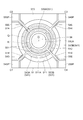
図2は、波長可変干渉フィルター5の概略構成を示す平面図であり、図3は、波長可変干渉フィルター5の断面図である。
波長可変干渉フィルター5は、図2に示すように、平面正方形状の板状の光学部材である。この波長可変干渉フィルター5は、図3に示すように、本発明に係る第一基板である固定基板51、および本発明に係る第二基板である可動基板52を備えている。これらの2枚の基板51,52は、それぞれ例えば、ソーダガラス、結晶性ガラス、石英ガラス、鉛ガラス、カリウムガラス、ホウケイ酸ガラス、無アルカリガラスなどの各種ガラスや、水晶などにより形成されている。そして、これらの2つの基板51,52は、外周部近傍に形成される接合部513,523が、例えば常温活性化接合やプラズマ重合膜を用いたシロキサン接合などにより、接合されることで、一体的に構成されている。
(3-1. Configuration of wavelength tunable interference filter)
FIG. 2 is a plan view showing a schematic configuration of the variable
As shown in FIG. 2, the wavelength
固定基板51には、本発明に係る第一反射膜を構成する固定反射膜56が設けられ、可動基板52には、本発明に係る第二反射膜を構成する可動反射膜57が設けられている。ここで、固定反射膜56は、固定基板51の可動基板52に対向する面に固定され、可動反射膜57は、可動基板52の固定基板51に対向する面に固定されている。また、これらの固定反射膜56および可動反射膜57は、ギャップを介して対向配置されている。
さらに、固定基板51と可動基板52との間には、固定反射膜56および可動反射膜57の間のギャップの寸法を調整するための静電アクチュエーター54が設けられている。この静電アクチュエーター54は、固定基板51側に設けられる第一駆動電極としての固定電極541と、可動基板52側に設けられる第二駆動電極としての可動駆動電極542とを備えている。
そして、固定基板51と可動基板52との間には、固定反射膜56および可動反射膜57の間のギャップを検出するためのギャップ検出センサー58が設けられている。このギャップ検出センサー58は、固定基板51側に設けられる本発明に係る第一検出電極としての固定検出電極551と、可動基板52側に設けられる本発明に係る第二検出電極としての可動検出電極552とを備えている。
The fixed
Further, an
A
(3−1−1.固定基板の構成)
図4は、第一実施形態の波長可変干渉フィルター5における固定基板51を可動基板52側から見た平面図である。
固定基板51は、厚みが例えば500μmに形成されるガラス基材を加工することで形成される。具体的には、図3に示すように、固定基板51には、エッチングにより電極形成溝511および反射膜固定部512が形成されている。この固定基板51は、可動基板52に対して厚み寸法が大きく形成されており、固定電極541および可動駆動電極542間に電圧を印加した際の静電引力や、固定電極541の内部応力による固定基板51の撓みはない。
(3-1-1. Configuration of Fixed Substrate)
FIG. 4 is a plan view of the fixed
The fixed
電極形成溝511は、図4に示すように、平面視で、固定基板51の平面中心点を中心とした円形に形成されている。反射膜固定部512は、前記平面視において、電極形成溝511の中心部から可動基板52側に突出して形成される。
また、固定基板51には、電極形成溝511から、固定基板51の外周縁の頂点C1,C3方向に向かって延出する一対の電極引出溝514が設けられている。
As shown in FIG. 4, the
In addition, the fixed
そして、固定基板51の電極形成溝511の溝底部である電極形成面511Aには、固定電極541が形成されている。
この固定電極541は、図4に示すように、固定反射膜56の中心点Oを中心とした仮想円Qの円周上に配置される円弧状の一対の固定部分電極(第一部分駆動電極を構成する第一固定部分電極543A、第二部分駆動電極を構成する第二固定部分電極543B)により構成されている。
これらの固定部分電極543A,543Bは、それぞれ、基板厚み方向から見た平面視における平面形状が同一で、略半円形状となる円弧状に形成され、かつ同一厚み寸法に形成されている。各固定部分電極543A,543Bの幅寸法(円弧の内径部と外径部との距離)は均一となっている。そして、これらの固定部分電極543A,543Bは、平面視において、固定反射膜56の中心点Oを中心とした仮想円Qの円周上で、中心点Oに対して互いに点対称となるように配置されている。
A fixed
As shown in FIG. 4, the fixed
These fixed
また、固定基板51には、第一固定部分電極543Aから延出する第一引出駆動電極545と、第二固定部分電極543Bから延出する第二引出駆動電極546と、を備えている。
第一引出駆動電極545は、第一固定部分電極543Aの外周縁から、図4における固定基板51の頂点C1方向に延出した電極引出溝514に沿って形成され、その先端部には、電圧制御部32に接続される第一駆動電極パッド545Pが設けられている。
また、第二引出駆動電極546は、第二固定部分電極543Bの外周縁から、図4における固定基板51の頂点C3方向に延出した電極引出溝514に沿って形成され、その先端部には、電圧制御部32に接続される第二駆動電極パッド546Pが設けられている。
さらに、これらの固定部分電極543A,543B上には、固定電極541および可動駆動電極542の間の放電を防止するための絶縁膜(図示略)が積層されている。
In addition, the fixed
The first
The second
Further, an insulating film (not shown) for preventing discharge between the fixed
反射膜固定部512は、上述したように、電極形成溝511と同軸上で、電極形成溝511よりも小さい径寸法となる円柱凹溝状に形成されている。なお、本実施形態では、図3に示すように、反射膜固定部512の可動基板52に対向する反射膜固定面512Aが、電極形成面511Aよりも可動基板52より放れて形成される例を示すが、これに限らない。電極形成面511Aおよび反射膜固定面512Aの高さ位置は、反射膜固定面512Aに固定される固定反射膜56、および可動基板52に形成される可動反射膜57の間のギャップの寸法、固定電極541および可動駆動電極542の間の寸法、固定反射膜56や可動反射膜57の厚み寸法により適宜設定される。したがって、例えば、電極形成面511Aと反射膜固定面512Aとが同一面に形成される構成や、電極形成面511Aの中心部に、円柱凸柱状の反射膜固定溝が形成され、この反射膜固定溝の底面に反射膜固定面が形成される構成などとしてもよい。
As described above, the reflective
そして、反射膜固定面512Aには、円形状に形成される固定反射膜56が固定されている。この固定反射膜56としては、金属の単層膜により形成されるものであってもよく、誘電体多層膜により形成されるものであってもよく、さらには、誘電多層膜上にAg合金が形成される構成などとしてもよい。金属単層膜としては、例えばAg合金の単層膜を用いることができ、誘電体多層膜の場合は、例えば高屈折層をTiO2、低屈折層をSiO2とした誘電体多層膜を用いることができる。
A fixed
さらに、反射膜固定面512Aには、本発明に係る固定検出電極551が固定されている。
この固定検出電極551は、図4に示すように、固定反射膜56の中心点Oを中心とした仮想円Rの円周上に配置される円弧状の一対の固定部分検出電極(本発明に係る第一部分検出電極を構成する第一固定部分検出電極553A、本発明に係る第二部分検出電極を構成する第二固定部分検出電極553B)により構成されている。
これらの固定部分検出電極553A,553Bは、それぞれ、基板厚み方向から見た平面視における平面形状が同一で、略半円形状となる円弧状に形成され、かつ同一厚み寸法に形成されている。各固定部分検出電極553A,553Bの幅寸法(円弧の内径部と外径部との距離)は均一となっている。そして、これらの固定部分検出電極553A,553Bは、平面視において、固定反射膜56の中心点Oを中心とした仮想円Rの円周上で、中心点Oに対して互いに点対称となるように配置されている。
Further, the fixed
As shown in FIG. 4, the fixed
These fixed
また、固定基板51には、第一固定部分検出電極553Aから延出する第一引出検出電極555と、第二固定部分検出電極553Bから延出する第二引出検出電極556と、を備えている。
第一引出検出電極555は、第一固定部分検出電極553Aの外周縁から、図4における固定基板51の頂点C2方向に延出した電極引出溝514に沿って形成され、その先端部には、ギャップ検出部33に接続される第一検出電極パッド555Pが設けられている。
また、第二引出検出電極556は、第二固定部分検出電極553Bの外周縁から、図4における固定基板51の頂点C4方向に延出した電極引出溝514に沿って形成され、その先端部には、ギャップ検出部33に接続される第二検出電極パッド556Pが設けられている。
The fixed
The first
Further, the second
さらに、固定基板51は、可動基板52に対向する面とは反対側の面において、固定反射膜56に対応する位置に図示略の反射防止膜が形成されている。この反射防止膜は、低屈折率膜および高屈折率膜を交互に積層することで形成され、固定基板51の表面での可視光の反射率を低下させ、透過率を増大させる。
Further, the fixed
(3−1−2.可動基板の構成)
図5は、第一実施形態の波長可変干渉フィルター5における可動基板52を固定基板51側から見た平面図である。
可動基板52は、厚みが例えば200μmに形成されるガラス基材をエッチングにより加工することで形成される。
具体的には、可動基板52は、図2、図5に示すような平面視において、基板中心点を中心とした円形の可動部521と、可動部521と同軸であり可動部521を保持する保持部522と、を備えている。
また、可動基板52は、図2および図5に示すように、第一駆動電極パッド545P、第二駆動電極パッド546P、第一検出電極パッド555Pおよび第二検出電極パッド556Pに対向する位置に、切欠部524を備えている。このような構成では、波長可変干渉フィルター5の可動基板52側から見た面に電極パッド545P、546P、555P、556Pが露出する。
(3-1-2. Configuration of movable substrate)
FIG. 5 is a plan view of the
The
Specifically, the
Further, as shown in FIGS. 2 and 5, the
可動部521は、保持部522よりも厚み寸法が大きく形成され、例えば、本実施形態では、可動基板52の厚み寸法と同一寸法である200μmに形成されている。また、可動部521は、反射膜固定部512に平行な可動面521Aを備え、この可動面521Aに、固定反射膜56とギャップを介して対向する可動反射膜57が固定されている。
ここで、この可動反射膜57は、上述した固定反射膜56と同一の構成の反射膜が用いられる。
The
Here, the movable
さらに、可動面521Aに、固定検出電極551とギャップを介して対向する本発明に係る可動検出電極552が固定されている。
この可動検出電極552は、図5に示すように、仮想円Rに沿い、内径寸法と外形寸法との差である幅寸法が仮想円Rの円周方向に沿って同一幅寸法となる円環状に形成されている。ここで、可動検出電極552は、図2に示すような基板厚み方向から見た平面視において、第一固定部分検出電極553Aと重なり合う第一対向検出領域554A、および第二固定部分検出電極553Bと重なり合う第二対向検出領域554Bを含む円環状に形成されている。そして、第一固定部分検出電極553Aと、可動検出電極552の第一対向検出領域554Aとにより、第一部分ギャップ検出センサー58Aが構成され、第二固定部分検出電極553Bと、可動検出電極552の第二対向検出領域554Bとにより、第二部分ギャップ検出センサー58Bが構成される。
Furthermore, the
As shown in FIG. 5, the
そして、可動部521は、可動面521Aとは反対側の面において、可動反射膜57に対応する位置に図示略の反射防止膜が形成されている。この反射防止膜は、固定基板51に形成される反射防止膜と同様の構成を有し、低屈折率膜および高屈折率膜を交互に積層することで形成される。
In the
保持部522は、可動部521の周囲を囲うダイヤフラムであり、例えば厚み寸法が50μmに形成され、可動部521よりも厚み方向に対する剛性が小さく形成されている。
このため、保持部522は可動部521よりも撓みやすく、僅かな静電引力により固定基板51側に撓ませることが可能となる。この際、可動部521は、保持部522よりも厚み寸法が大きく、剛性が大きくなるため、静電引力により可動基板52を撓ませる力が作用した場合でも、可動部521の撓みはほぼなく、可動部521に形成された可動反射膜57の撓みも防止できる。
The holding
For this reason, the holding
そして、この保持部522の固定基板51に対向する面には、固定電極541と、初期状態において約1μmの隙間を介して対向する、可動駆動電極542が固定されている。
この可動駆動電極542は、図5に示すように、仮想円Qに沿い、内径寸法と外形寸法との差である幅寸法が仮想円Qの円周方向に沿って同一幅寸法となる円環状に形成されている。ここで、可動駆動電極542は、図2に示すような基板厚み方向から見た平面視において、第一固定部分電極543Aと重なり合う第一対向駆動領域544A、および第二固定部分電極543Bと重なり合う第二対向駆動領域544Bを含む円環状に形成されている。そして、第一固定部分電極543Aと、可動駆動電極542の第一対向駆動領域544Aとにより、第一部分アクチュエーター55Aが構成され、第二固定部分電極543Bと、可動駆動電極542の第二対向駆動領域544Bとにより、第二部分アクチュエーター55Bが構成される。
A
As shown in FIG. 5, the
(3−1−3.静電アクチュエーターの構成)
図6は、第一実施形態の静電アクチュエーター54の配線図である。
静電アクチュエーター54は、上述したように、第一固定部分電極543Aおよび可動駆動電極542の第一対向駆動領域544Aにより構成される第一部分アクチュエーター55Aと、第二固定部分電極543Bおよび可動駆動電極542の第二対向駆動領域544Bにより構成される第二部分アクチュエーター55Bと、を備えている。
(3-1-3. Structure of electrostatic actuator)
FIG. 6 is a wiring diagram of the
As described above, the
このような静電アクチュエーター54では、第一引出駆動電極545の第一駆動電極パッド545Pと、第二引出駆動電極546の第二駆動電極パッド546Pとの間に駆動電圧Vが印加されると、各部分アクチュエーター55A,55Bには、容量リアクタンスに応じた分圧V1,V2が印加される。
また、各部分アクチュエーター55A,55Bは、波長可変干渉フィルター5を基板厚み方向から見た平面視において、同一形状に形成され、仮想円Q上で等角度間隔(180度)に配置されている。したがって、各部分アクチュエーター55A,55Bにおける電極間の寸法(電極間ギャップ)をそれぞれd1、d2、第一及び第二固定部分電極543A,543B、第一対向駆動領域544A、および第二対向駆動領域544Bの面積をSD、誘電率をεとすると、各部分アクチュエーター55A,55Bの静電容量CD1,CD2はそれぞれ、以下の式(1)〜(2)で表される。
In such an
In addition, the
CD1=εSD/d1 …(1)
CD2=εSD/d2 …(2)
C D1 = εS D / d 1 (1)
C D2 = εS D / d 2 (2)
ここで、各部分アクチュエーター55A,55Bは、電気的に直列接続されているため、これらの部分アクチュエーター55A,55Bで保持される電荷量Qは同値となり、以下の式(3)が成立する。
Here, since the
Q=CD1V1=CD2V2 …(3) Q = C D1 V 1 = C D2 V 2 (3)
一方、各部分アクチュエーター55A,55Bに作用する静電引力F1,F2は、各部分アクチュエーター55A,55Bの電極間の電界E1,E2と、各部分アクチュエーター55A,55Bで保持される電荷量Qとの積E1Q,E2Qとなる。
したがって、静電引力F1,F2は、上記式(1)〜(3)を代入すると、以下の式(4)〜(5)のように表せる。
On the other hand, the electrostatic attractive forces F 1 and F 2 acting on the
Therefore, the electrostatic attractive forces F 1 and F 2 can be expressed as the following expressions (4) to (5) when the above expressions (1) to (3) are substituted.
F1=E1Q=Q2/εSD …(4)
F2=E2Q=Q2/εSD …(5)
F 1 = E 1 Q = Q 2 / εS D ... (4)
F 2 = E 2 Q = Q 2 / εS D ... (5)
すなわち、上記式(4)〜(5)に示されるように、各部分アクチュエーター55A,55Bに作用する静電引力F1,F2は、部分電極間ギャップd1、d2の値によらず同値となる。
したがって、例えば、初期ギャップにおいて、電極間ギャップd1、d2の値に、例えば測定精度に影響しない程度の僅かな差があり、静電アクチュエーター54に電圧を印加した場合であっても、これらの電極間ギャップd1、d2の差が開くことがなく、保持部522を均一に撓ませることができる。
That is, as shown in the above formulas (4) to (5), the electrostatic attractive forces F 1 and F 2 acting on the
Therefore, for example, in the initial gap, the values of the gaps d 1 and d 2 between the electrodes have a slight difference that does not affect the measurement accuracy, for example, and even when a voltage is applied to the
(3−1−4.ギャップ検出センサーの構成)
図7は、第一実施形態のギャップ検出センサー58の配線図である。
ギャップ検出センサー58は、上述したように、第一固定部分検出電極553Aおよび可動検出電極552の第一対向検出領域554Aにより構成される第一部分ギャップ検出センサー58Aと、第二固定部分検出電極553Bおよび可動検出電極552の第二対向検出領域554Bにより構成される第二部分ギャップ検出センサー58Bと、を備えている。
(3-1-4. Configuration of Gap Detection Sensor)
FIG. 7 is a wiring diagram of the
As described above, the
各部分ギャップ検出センサー58A、58Bは、波長可変干渉フィルター5を基板厚み方向から見た平面視において、同一形状に形成され、仮想円R上で等角度間隔(180度)に配置されている。したがって、各部分ギャップ検出センサー58A、58Bにおける検出電極間の寸法(検出電極間ギャップ)をそれぞれh1、h2、第一及び第二固定部分検出電極553A、553B、第一対向検出領域554A、および第二対向検出領域554Bの面積をSS、誘電率をεとすると、各部分ギャップ検出センサー58A,58Bの静電容量CS1,CS2はそれぞれ、以下の式(6)〜(7)で表される。
The partial
CS1=εSS/h1 …(6)
CS2=εSS/h2 …(7)
C S1 = εS S / h 1 (6)
C S2 = εS S / h 2 (7)
このようなギャップ検出センサー58では、第一引出検出電極555の第一検出電極パッド555Pと、第二引出検出電極556の第二検出電極パッド556Pとの間の静電容量CSは、以下の式(8)で表される。
In such a
CS=CS1CS2/(CS1+CS2)=εSS/(h1+h2) …(8) C S = C S1 C S2 / (C S1 + C S2 ) = εS S / (h 1 + h 2 ) (8)
そして、検出電極間の平均寸法hは、以下の式(9)で表される。 And the average dimension h between detection electrodes is represented by the following formula | equation (9).
h=(h1+h2)/2=εSS/2CS …(9) h = (h 1 + h 2 ) / 2 = εS S / 2C S (9)
したがって、第一引出検出電極555の第一検出電極パッド555Pと、第二引出検出電極556の第二検出電極パッド556Pとの間の静電容量CSを測定することで検出電極間の平均寸法hを検出することができる。
なお、本実施形態では、第一検出電極と第一反射膜と、は同一面上に設けられ、第二検出電極と第二反射膜と、も同一面上に設けられている。このため、第一反射膜と第二反射膜間のギャップと第一検出電極と第二検出電極間のギャップは等しくなり、反射膜間のギャップを高精度に検出することができる。
Accordingly, the first
In the present embodiment, the first detection electrode and the first reflection film are provided on the same surface, and the second detection electrode and the second reflection film are also provided on the same surface. For this reason, the gap between the first reflection film and the second reflection film and the gap between the first detection electrode and the second detection electrode are equal, and the gap between the reflection films can be detected with high accuracy.
(3−1−5.波長可変干渉フィルターへの配線)
図8は、波長可変干渉フィルター5を測色センサー3に組み込んだ際の配線構造を示す図である。図9は、波長可変干渉フィルター5を測色センサー3に組み込んだ際の配線構造の他の例を示す図である。
(3-1-5. Wiring to wavelength variable interference filter)
FIG. 8 is a diagram showing a wiring structure when the variable
波長可変干渉フィルター5を測色センサー3に組み込む場合、一般には、測色センサー3に設けられたフィルター固定基板に直接波長可変干渉フィルター5を固定したり、ケースに波長可変干渉フィルター5を保持し、ケースをフィルター固定基板に固定したりする。
When the wavelength
そして、波長可変干渉フィルター5の電極パッド545P、546Pと、測色センサー3の電圧制御部32とを接続する場合、及び、波長可変干渉フィルター5の電極パッド555P、556Pと、測色センサー3のギャップ検出部33とを接続する場合、波長可変干渉フィルター5が固定部34に固定された状態で配線が施される。
この時、波長可変干渉フィルター5への配線方法としては、例えば、図8に示すように、電極パッド545P、546P、555P、556P上に溶融状態のAgペースト等の導電性部材35を設け、導電性部材35が固化する前に、波長可変干渉フィルター5の可動基板52側から、リード線36を接続する。この場合、配線作業を、波長可変干渉フィルター5の可動基板52側から容易にリード線36を接続することができる。
When the
At this time, as a wiring method to the wavelength
また、波長可変干渉フィルター5への他の配線方法としては、例えば、図9に示すように、FPC37(Flexible Printed Circuits)を、異方性導電フィルム(ACF:Anisotropic Conductive Film)または、異方性導電ペースト(ACP:Anisotropic Conductive Paste)等の異方性導電層38を介して接続してもよい。この場合、電極パッド545P、546P、555P、556P上に異方性導電層38を形成し、FPC37を被せた後、波長可変干渉フィルター5の可動基板52側からFPC37を押圧する。この場合でも、可動基板52に応力が加わらないため、固定基板51と可動基板52との剥離や、可動基板52の撓みなどがなく、波長可変干渉フィルター5の性能を維持することができる。
As another wiring method to the wavelength
(3−2.電圧制御手段の構成)
電圧制御部32は、制御装置4からの入力される制御信号に基づいて、静電アクチュエーター54に印加する電圧を制御する。
(3-2. Configuration of voltage control means)
The
(3−3.ギャップ検出手段の構成)
ギャップ検出部33は、波長可変干渉フィルター5のギャップ検出センサー58の静電容量を検出し、検出信号を制御装置4へ出力する。
(3-3. Configuration of Gap Detection Unit)
The
〔4.制御装置の構成〕
制御装置4は、測色装置1の全体動作を制御する。
この制御装置4としては、例えば汎用パーソナルコンピューターや、携帯情報端末、その他、測色専用コンピューターなどを用いることができる。
そして、制御装置4は、図1に示すように、光源制御部41、測色センサー制御部42、および本発明に係る分析処理部を構成する測色処理部43などを備えて構成されている。
光源制御部41は、光源装置2に接続されている。そして、光源制御部41は、例えば利用者の設定入力に基づいて、光源装置2に所定の制御信号を出力し、光源装置2から所定の明るさの白色光を射出させる。
測色センサー制御部42は、測色センサー3に接続されている。そして、測色センサー制御部42は、例えば利用者の設定入力に基づいて、測色センサー3にて受光させる光の波長を設定し、この波長の光の受光量を検出する旨の制御信号を測色センサー3に出力する。このとき、測色センサー制御部42は測色センサー3のギャップ検出部33の検出信号に基づいて制御信号を補正することができる。これにより、測色センサー3の電圧制御部32は、制御信号に基づいて、利用者が所望する光の波長のみを透過させるよう、静電アクチュエーター54への印加電圧を設定する。
測色処理部43は、検出部31により検出された受光量から、測定対象Aの色度を分析する。
[4. Configuration of control device]
The
As the
As shown in FIG. 1, the
The light
The colorimetric
The
〔5.本実施形態の作用効果〕
上述したように、上記実施形態の波長可変干渉フィルター5は、固定電極541が互いに絶縁された第一固定部分電極543Aおよび第二固定部分電極543Bにより構成され、可動駆動電極542は、第一固定部分電極543Aに対向する第一対向駆動領域544Aおよび第二固定部分電極543Bに対向する第二対向駆動領域544Bを含むリング状に形成されている。そして、第一固定部分電極543Aには第一引出駆動電極545が形成され、第二固定部分電極543Bには第二引出駆動電極546が形成されている。
このような構成では、第一引出駆動電極545の第一駆動電極パッド545Pと、第二引出駆動電極546の第二駆動電極パッド546Pとの間に駆動電圧を印加することで、第一固定部分電極543Aおよび可動駆動電極542の第一対向駆動領域544Aにより構成された第一部分アクチュエーター55Aと、第二固定部分電極543Bおよび可動駆動電極542の第二対向駆動領域544Bにより構成された第二部分アクチュエーター55Bを駆動させることができる。
[5. Effects of this embodiment]
As described above, the wavelength
In such a configuration, by applying a driving voltage between the first
さらに、固定検出電極551が互いに絶縁された第一固定部分検出電極553Aおよび第二固定部分検出電極553Bにより構成され、可動検出電極552は、第一固定部分検出電極553Aに対向する第一対向検出領域554Aおよび第二固定部分検出電極553Bに対向する第二対向検出領域554Bを含むリング状に形成されている。そして、第一固定部分検出電極553Aには第一引出検出電極555が形成され、第二固定部分検出電極553Bには第二引出検出電極556が形成されている。
このような構成では、第一引出検出電極555の第一検出電極パッド555Pと、第二引出検出電極556の第二検出電極パッド556Pとの間の静電容量を検出することで、反射膜56,57間のギャップ寸法を検出することができる。
Further, the fixed
In such a configuration, the
そして、第一引出駆動電極545、および第二引出駆動電極546は、固定基板51上に形成され、それぞれ固定基板51の外周縁に形成された第一駆動電極パッド545P、および第二駆動電極パッド546Pに接続されている。
また、第一引出検出電極555、および第二引出検出電極556は、固定基板51上に形成され、それぞれ固定基板51の外周縁に形成された第一検出電極パッド555P、および第二検出電極パッド556Pに接続されている。
このため、波長可変干渉フィルター5を測色センサー3に組み込む際、Agペーストなどの導電性部材35を介してリード線36を接続する際でも、異方性導電層38を介してFPC37を接続する際でも、波長可変干渉フィルター5の可動基板52側から配線作業を簡単に実施できる。また、配線により、固定部34に固定される固定基板51に対して応力が加わることがあったとしても、可動基板52には応力が加わらないので、固定基板51および可動基板52の剥離や、可動基板52の傾斜が発生せず、波長可変干渉フィルターの性能低下を防止できる。また、固定基板51の各電極パッド545P、546P、555P、556Pに対して確実に配線することができるので、配線信頼性が向上し、測色センサー3や測色装置1の信頼性をも向上させることができる。
The first
The first
For this reason, when the variable
また、可動基板52には、電極パッド545P、546P、555P、556Pの位置に対応して切欠部524が形成されている。このため、配線作業時に、可動基板52が邪魔になることがない。また、可動基板52に応力を加えることなく配線を実施できる。
Further, the
また、各部分アクチュエーター55A,55Bにおける、仮想円Qの周方向および基板厚み方向に対して直交する幅寸法は、均一に形成されている。このため、各部分アクチュエーター55A,55Bにおいて、周方向に沿った静電引力のムラがなく、可動部521を精度よく変位させることができる。
Further, in each of the
そして、固定電極541の第一固定部分電極543Aおよび第二固定部分電極543Bは、平面視において同一形状に形成されており、仮想円Qの円周上で、中心点Oに対して点対称となる位置に配置されている。また、第一固定部分電極543Aおよび第一対向駆動領域544Aにより構成された第一部分アクチュエーター55Aと、第二固定部分電極543Bおよび第二対向駆動領域544Bにより構成された第二部分アクチュエーター55Bとは、電気的に直列に接続されている。
このため、静電アクチュエーター54に駆動電圧を印加した際に、各部分アクチュエーター55A,55Bに同一大きさの静電引力が作用する。したがって、固定反射膜56および可動反射膜57間のギャップを変動させた場合でも、固定反射膜56および可動反射膜57の平行性を維持することができ、分解能の低下を抑えることができる。
The first fixed
For this reason, when a drive voltage is applied to the
さらに、可動駆動電極542は、可動基板52の保持部522上で、仮想円Qの円周に沿うリング上に形成されている。すなわち、可動部521の中心点に対して点対称となる形状に形成されている。さらには、可動基板52には、可動駆動電極542から延出する引出電極等が不要であり、引出電極による膜応力なども発生しない。
このため、保持部522に作用する可動駆動電極542の膜応力が均一となり、保持部522の応力バランスを均一に保つことができ、可動部521の傾斜を抑えることができる。したがって、反射膜56,57間のギャップ寸法を均一にすることができ、波長可変干渉フィルター5の分解能を高精度に維持することができる。
Furthermore, the
Therefore, the film stress of the
1…光分析装置としての測色装置、3…光モジュールとしての測色センサー、5…波長可変干渉フィルター、31…検出部、43…分析処理部である測色処理部、51…第一基板である固定基板、52…第二基板である可動基板、54…静電アクチュエーター、55A…第一部分アクチュエーター、55B…第二部分アクチュエーター、56…第一反射膜である固定反射膜、57…第二反射膜である可動反射膜、58…ギャップ検出センサー、58A…第一部分ギャップ検出センサー、58B…第二部分ギャップ検出センサー、521…可動部、522…保持部、541…第一駆動電極である固定駆動電極、542…第二駆動電極である可動駆動電極、543A…第一部分駆動電極である第一固定部分駆動電極、543B…第二部分駆動電極である第二固定部分駆動電極、544A…第一対向駆動領域、544B…第二対向駆動領域、545…第一引出駆動電極、546…第二引出駆動電極、551…第一検出電極である固定検出電極、552…第二検出電極である可動検出電極、553A…第一部分検出電極である第一固定部分検出電極、553B…第二部分検出電極である第二固定部分検出電極、554A…第一対向検出領域、554B…第二対向検出領域、555…第一引出検出電極、556…第二引出検出電極。
DESCRIPTION OF SYMBOLS 1 ... Color measuring device as an optical analyzer, 3 ... Color measuring sensor as an optical module, 5 ... Wavelength variable interference filter, 31 ... Detection part, 43 ... Color measuring process part which is an analysis process part, 51 ... 1st board | substrate A fixed
Claims (9)
前記第一基板に対向する第二基板と、
前記第一基板に設けられた第一反射膜と、
前記第二基板に設けられ、前記第一反射膜とギャップを介して対向する第二反射膜と、
前記第一基板に設けられた第一駆動電極、および前記第二基板に設けられて前記第一駆動電極に対向する第二駆動電極を備えた静電アクチュエーターと、
前記第一基板に設けられた第一検出電極、および前記第二基板に設けられて前記第一検出電極に対向する第二検出電極を備えたギャップ検出電極と、
を具備し、
前記第二基板は、前記第一基板および前記第二基板を基板厚み方向から見た平面視において、円形状に設けられ前記第二反射膜が設けられた可動部と、前記可動部を前記第一基板に対して進退可能に保持する保持部と、を備え、
前記第一検出電極は、前記平面視において、前記可動部の中心点を中心とした仮想円に沿って設けられた第一部分検出電極および第二部分検出電極を備え、
前記第二検出電極は、前記平面視において、前記第一部分検出電極に重なる第一対向検出領域と、前記第二部分検出電極に重なる第二対向検出領域とを備え、
前記第一部分電極に電気的に接続される第一電極と、前記第二部分検出電極に電気的に接続される第二電極と、の間の静電容量を測定することにより、前記ギャップの検出が行われることを特徴とする波長可変干渉フィルター。 A first substrate;
A second substrate facing the first substrate;
A first reflective film provided on the first substrate;
A second reflective film provided on the second substrate and facing the first reflective film via a gap;
An electrostatic actuator comprising a first drive electrode provided on the first substrate and a second drive electrode provided on the second substrate and facing the first drive electrode;
A first detection electrode provided on the first substrate, and a gap detection electrode including a second detection electrode provided on the second substrate and facing the first detection electrode;
Comprising
The second substrate includes a movable portion provided in a circular shape and provided with the second reflective film in a plan view of the first substrate and the second substrate as viewed from the substrate thickness direction, and the movable portion as the first substrate. A holding portion that holds the substrate so as to be capable of moving forward and backward,
The first detection electrode includes a first partial detection electrode and a second partial detection electrode provided along a virtual circle centered on a central point of the movable part in the plan view,
The second detection electrode includes a first opposing detection region that overlaps the first partial detection electrode and a second opposing detection region that overlaps the second partial detection electrode in the plan view ,
Detection of the gap by measuring a capacitance between a first electrode electrically connected to the first partial electrode and a second electrode electrically connected to the second partial detection electrode A tunable interference filter characterized in that is performed .
前記第一基板には、前記第一部分検出電極から前記第一基板の外周縁に向かって延出する第一引出検出電極と、前記第二部分検出電極から前記第一基板の外周縁に向かって延出する第二引出検出電極とが設けられていることを特徴とする波長可変干渉フィルター。 The tunable interference filter according to claim 1,
The first substrate includes a first extraction detection electrode extending from the first partial detection electrode toward the outer peripheral edge of the first substrate, and the second partial detection electrode toward the outer peripheral edge of the first substrate. A tunable interference filter, characterized in that an extended second extraction detection electrode is provided.
前記第一駆動電極は、前記平面視において、前記可動部の中心点を中心とした仮想円に沿って設けられた第一部分駆動電極および第二部分駆動電極を備え、
前記第二駆動電極は、前記平面視において、前記第一部分駆動電極に重なる第一対向駆動領域と、前記第二部分駆動電極に重なる第二対向駆動領域とを備え、
前記第一基板には、前記第一部分駆動電極から前記第一基板の外周縁に向かって延出する第一引出駆動電極と、前記第二部分駆動電極から前記第一基板の外周縁に向かって延出する第二引出駆動電極とが設けられたことを特徴とする波長可変干渉フィルター。 In the wavelength tunable interference filter according to claim 1 or 2,
The first drive electrode includes a first partial drive electrode and a second partial drive electrode provided along a virtual circle centered on a central point of the movable part in the plan view,
The second drive electrode includes a first counter drive region that overlaps the first partial drive electrode and a second counter drive region that overlaps the second partial drive electrode in the plan view,
The first substrate includes a first extraction drive electrode extending from the first partial drive electrode toward the outer periphery of the first substrate, and a second partial drive electrode toward the outer periphery of the first substrate. A variable wavelength interference filter, characterized in that an extended second extraction drive electrode is provided.
前記第一検出電極は、前記第一反射膜と同一面上に設けられ、
前記第二検出電極は、前記第二反射膜と同一面上に設けられたことを特徴とする波長可変干渉フィルター。 In the wavelength tunable interference filter according to any one of claims 1 to 3,
The first detection electrode is provided on the same plane as the first reflective film,
The variable wavelength interference filter, wherein the second detection electrode is provided on the same plane as the second reflective film.
前記第一部分検出電極は、第一仮想円に沿う円弧形状であり、
前記第二部分検出電極は、前記第一仮想円に沿う円弧形状であり、前記平面視において、前記第一部分検出電極と同一形状に形成され、かつ、前記可動部の中心点に対し、前記第一部分検出電極と点対称となる位置に設けられたことを特徴とする波長可変干渉フィルター。 In the wavelength variable interference filter according to any one of claims 1 to 4,
The first partial detection electrode has an arc shape along a first virtual circle,
The second partial detection electrode has an arc shape along the first virtual circle, and is formed in the same shape as the first partial detection electrode in the plan view, and the second partial detection electrode is formed with respect to the center point of the movable part. A wavelength tunable interference filter characterized in that a part of the wavelength tunable interference filter is provided at a position that is point-symmetric with respect to a detection electrode.
前記第一基板に対向する第二基板と、
前記第一基板に設けられた第一反射膜と、
前記第二基板に設けられ、前記第一反射膜とギャップを介して対向する第二反射膜と、
前記第一基板に設けられた第一部分検出電極と前記第二基板に設けられた第二検出電極とが対向する第一検出容量部、及び前記第一基板に設けられた第二部分検出電極と前記第二検出電極とが対向する第二検出容量部を有するギャップ検出電極と、
を備え、
前記第一検出容量部と前記第二検出容量部とが電気的に直列に接続され、
前記第一部分電極に電気的に接続される第一電極と、前記第二部分検出電極に電気的に接続される第二電極と、の間の静電容量を測定することにより、前記ギャップの検出が行われることを特徴とする波長可変干渉フィルター。 A first substrate;
A second substrate facing the first substrate;
A first reflective film provided on the first substrate;
A second reflective film provided on the second substrate and facing the first reflective film via a gap;
A first detection capacitor portion on which the first partial detection electrode provided on the first substrate and a second detection electrode provided on the second substrate face each other; and a second partial detection electrode provided on the first substrate; A gap detection electrode having a second detection capacitance portion opposed to the second detection electrode;
With
The first detection capacitor unit and the second detection capacitor unit are electrically connected in series ,
Detection of the gap by measuring a capacitance between a first electrode electrically connected to the first partial electrode and a second electrode electrically connected to the second partial detection electrode A tunable interference filter characterized in that is performed .
平面視において、前記第二検出電極は円環状であることを特徴とする波長可変干渉フィルター。 The wavelength variable interference filter according to claim 2, wherein the second detection electrode has an annular shape in plan view.
前記波長可変干渉フィルターにより取り出された光を検出する検出部と、
を具備したことを特徴とする光モジュール。 The wavelength variable interference filter according to any one of claims 1 to 7 ,
A detection unit for detecting light extracted by the wavelength variable interference filter;
An optical module comprising:
前記光モジュールの前記検出部により検出された光に基づいて、前記光の光特性を分析する分析処理部と、
を具備したことを特徴とする光分析装置。 An optical module according to claim 8 ,
Based on the light detected by the detection unit of the optical module, an analysis processing unit for analyzing the light characteristics of the light;
An optical analyzer characterized by comprising:
Priority Applications (2)
| Application Number | Priority Date | Filing Date | Title |
|---|---|---|---|
| JP2011085172A JP5724557B2 (en) | 2011-04-07 | 2011-04-07 | Tunable interference filter, optical module, and optical analyzer |
| US13/441,342 US9482857B2 (en) | 2011-04-07 | 2012-04-06 | Tunable interference filter, optical module, and photometric analyzer |
Applications Claiming Priority (1)
| Application Number | Priority Date | Filing Date | Title |
|---|---|---|---|
| JP2011085172A JP5724557B2 (en) | 2011-04-07 | 2011-04-07 | Tunable interference filter, optical module, and optical analyzer |
Publications (3)
| Publication Number | Publication Date |
|---|---|
| JP2012220656A JP2012220656A (en) | 2012-11-12 |
| JP2012220656A5 JP2012220656A5 (en) | 2014-05-22 |
| JP5724557B2 true JP5724557B2 (en) | 2015-05-27 |
Family
ID=46965891
Family Applications (1)
| Application Number | Title | Priority Date | Filing Date |
|---|---|---|---|
| JP2011085172A Expired - Fee Related JP5724557B2 (en) | 2011-04-07 | 2011-04-07 | Tunable interference filter, optical module, and optical analyzer |
Country Status (2)
| Country | Link |
|---|---|
| US (1) | US9482857B2 (en) |
| JP (1) | JP5724557B2 (en) |
Families Citing this family (9)
| Publication number | Priority date | Publication date | Assignee | Title |
|---|---|---|---|---|
| JP5673075B2 (en) * | 2010-12-21 | 2015-02-18 | セイコーエプソン株式会社 | Tunable interference filter, optical module, and optical analyzer |
| JP5919728B2 (en) * | 2011-10-26 | 2016-05-18 | セイコーエプソン株式会社 | Spectrometer |
| JP5811789B2 (en) * | 2011-11-09 | 2015-11-11 | セイコーエプソン株式会社 | Spectrometer |
| JP6098051B2 (en) | 2012-07-04 | 2017-03-22 | セイコーエプソン株式会社 | Spectrometer |
| JP2015066611A (en) * | 2013-09-27 | 2015-04-13 | セイコーエプソン株式会社 | Actuator drive system, optical module, and electronic equipment |
| JP2015177564A (en) * | 2014-03-13 | 2015-10-05 | パイオニア株式会社 | actuator |
| JP6115519B2 (en) * | 2014-05-27 | 2017-04-19 | セイコーエプソン株式会社 | MEMS driving device, electronic device, and MEMS driving method |
| CN112424574A (en) * | 2018-05-17 | 2021-02-26 | 尤尼斯拜特罗有限责任公司 | Optical device and bonding method |
| JP2020171191A (en) * | 2020-06-03 | 2020-10-15 | パイオニア株式会社 | Actuator |
Family Cites Families (19)
| Publication number | Priority date | Publication date | Assignee | Title |
|---|---|---|---|---|
| JPH0194312A (en) * | 1987-10-06 | 1989-04-13 | Sharp Corp | Variable interference device |
| FR2768812B1 (en) | 1997-09-19 | 1999-10-22 | Commissariat Energie Atomique | FABRY-PEROT INTERFEROMETER TUNABLE INTEGRATED |
| US5914804A (en) * | 1998-01-28 | 1999-06-22 | Lucent Technologies Inc | Double-cavity micromechanical optical modulator with plural multilayer mirrors |
| JP3450180B2 (en) * | 1998-04-20 | 2003-09-22 | 日本電気株式会社 | Tunable laser |
| JP2002071562A (en) | 2000-09-04 | 2002-03-08 | Yokogawa Electric Corp | Infrared spectrometric apparatus |
| JP3835525B2 (en) | 2001-03-19 | 2006-10-18 | ホーチキ株式会社 | Wavelength tunable filter controller |
| GB2375184A (en) * | 2001-05-02 | 2002-11-06 | Marconi Caswell Ltd | Wavelength selectable optical filter |
| JP4548245B2 (en) * | 2005-06-27 | 2010-09-22 | セイコーエプソン株式会社 | Tunable filter |
| JP4548288B2 (en) | 2005-09-22 | 2010-09-22 | セイコーエプソン株式会社 | Tunable filter |
| JP4466634B2 (en) | 2006-01-19 | 2010-05-26 | セイコーエプソン株式会社 | Optical device, wavelength tunable filter, wavelength tunable filter module, and optical spectrum analyzer |
| JP4379457B2 (en) | 2006-01-19 | 2009-12-09 | セイコーエプソン株式会社 | Optical device, wavelength tunable filter, wavelength tunable filter module, and optical spectrum analyzer |
| CN100538432C (en) | 2006-01-19 | 2009-09-09 | 精工爱普生株式会社 | Wave length variable filter, wave length variable filter module and optical spectrum analyser |
| GB2445956B (en) * | 2007-01-26 | 2009-12-02 | Valtion Teknillinen | A spectrometer and a method for controlling the spectrometer |
| JP2008183350A (en) * | 2007-01-31 | 2008-08-14 | Olympus Corp | Variable spectroscopic element, spectroscopic device and endoscopic system |
| FI125817B (en) * | 2009-01-27 | 2016-02-29 | Teknologian Tutkimuskeskus Vtt Oy | Improved electronically controlled Fabry-Perot interferometer, an intermediate product, an electrode system and a method for producing an electronically controlled Fabry-Perot interferometer |
| JP2010224011A (en) | 2009-03-19 | 2010-10-07 | Olympus Corp | Etalon device and optical unit equipped with the same |
| JP4831242B2 (en) | 2010-05-28 | 2011-12-07 | セイコーエプソン株式会社 | Tunable filter |
| JP4831244B2 (en) | 2010-05-28 | 2011-12-07 | セイコーエプソン株式会社 | Tunable filter |
| JP4831243B2 (en) | 2010-05-28 | 2011-12-07 | セイコーエプソン株式会社 | Tunable filter |
-
2011
- 2011-04-07 JP JP2011085172A patent/JP5724557B2/en not_active Expired - Fee Related
-
2012
- 2012-04-06 US US13/441,342 patent/US9482857B2/en not_active Expired - Fee Related
Also Published As
| Publication number | Publication date |
|---|---|
| JP2012220656A (en) | 2012-11-12 |
| US20120257205A1 (en) | 2012-10-11 |
| US9482857B2 (en) | 2016-11-01 |
Similar Documents
| Publication | Publication Date | Title |
|---|---|---|
| JP5724557B2 (en) | Tunable interference filter, optical module, and optical analyzer | |
| US10473913B2 (en) | Variable wavelength interference filter, optical module, and optical analysis device | |
| US9664890B2 (en) | Variable wavelength interference filter, optical module, and optical analyzer | |
| JP5779852B2 (en) | Tunable interference filter, optical module, and optical analyzer | |
| JP5673049B2 (en) | Wavelength variable interference filter, optical module, and optical analyzer | |
| JP5707780B2 (en) | Wavelength variable interference filter, optical module, and optical analyzer | |
| US20140240513A1 (en) | Spectroscopic camera and spectroscopic image processing method | |
| JP2012150353A (en) | Wavelength variable interference filter, optical module, and optical analysis device | |
| JP2011053510A (en) | Wavelength variable interference filter, colorimetry sensor, colorimetry module and method of controlling wavelength variable interference filter | |
| JP2013072930A (en) | Wavelength variable interference filter, optical filter device, optical module and electronic apparatus | |
| JP5445303B2 (en) | Optical filter element, optical filter module, and analytical instrument | |
| US20140285799A1 (en) | Spectroscopic camera and alignment adjustment method | |
| JP5673075B2 (en) | Tunable interference filter, optical module, and optical analyzer | |
| JP5617621B2 (en) | Wavelength variable interference filter, optical module, and optical analyzer | |
| JP5999213B2 (en) | Wavelength variable interference filter, optical module, and optical analyzer | |
| JP2012088419A (en) | Optical module and optical analysis device | |
| JP2012047858A (en) | Wavelength variable interference filter, optical module, optical analyzer, and manufacturing method of wavelength variable interference filter | |
| JP2012141347A (en) | Wavelength variable interference filter, optical module, and optical analyzer | |
| JP2012150193A (en) | Wavelength variable interference filter, optical module and optical analysis device | |
| JP2016090251A (en) | Spectrometer and spectrometric method | |
| JP2012128136A (en) | Optical sensor | |
| JP5884393B2 (en) | Wavelength variable interference filter, optical filter device, optical module, and electronic apparatus | |
| JP5673117B2 (en) | Optical module and optical analyzer | |
| JP2016095526A (en) | Wavelength variable interference filter, optical module and optical analysis device |
Legal Events
| Date | Code | Title | Description |
|---|---|---|---|
| A521 | Written amendment |
Free format text: JAPANESE INTERMEDIATE CODE: A523 Effective date: 20140401 |
|
| A621 | Written request for application examination |
Free format text: JAPANESE INTERMEDIATE CODE: A621 Effective date: 20140401 |
|
| A131 | Notification of reasons for refusal |
Free format text: JAPANESE INTERMEDIATE CODE: A131 Effective date: 20141216 |
|
| A977 | Report on retrieval |
Free format text: JAPANESE INTERMEDIATE CODE: A971007 Effective date: 20141217 |
|
| RD04 | Notification of resignation of power of attorney |
Free format text: JAPANESE INTERMEDIATE CODE: A7424 Effective date: 20150106 |
|
| A521 | Written amendment |
Free format text: JAPANESE INTERMEDIATE CODE: A523 Effective date: 20150213 |
|
| TRDD | Decision of grant or rejection written | ||
| A01 | Written decision to grant a patent or to grant a registration (utility model) |
Free format text: JAPANESE INTERMEDIATE CODE: A01 Effective date: 20150303 |
|
| A61 | First payment of annual fees (during grant procedure) |
Free format text: JAPANESE INTERMEDIATE CODE: A61 Effective date: 20150316 |
|
| R150 | Certificate of patent or registration of utility model |
Ref document number: 5724557 Country of ref document: JP Free format text: JAPANESE INTERMEDIATE CODE: R150 |
|
| S531 | Written request for registration of change of domicile |
Free format text: JAPANESE INTERMEDIATE CODE: R313531 |
|
| R350 | Written notification of registration of transfer |
Free format text: JAPANESE INTERMEDIATE CODE: R350 |
|
| LAPS | Cancellation because of no payment of annual fees |