EP0902874B1 - Interferometre destine a la mesure des variations d'epaisseur de plaquettes de semi-conducteurs - Google Patents
Interferometre destine a la mesure des variations d'epaisseur de plaquettes de semi-conducteurs Download PDFInfo
- Publication number
- EP0902874B1 EP0902874B1 EP97927809A EP97927809A EP0902874B1 EP 0902874 B1 EP0902874 B1 EP 0902874B1 EP 97927809 A EP97927809 A EP 97927809A EP 97927809 A EP97927809 A EP 97927809A EP 0902874 B1 EP0902874 B1 EP 0902874B1
- Authority
- EP
- European Patent Office
- Prior art keywords
- test piece
- parallel
- light source
- beams
- parallel surfaces
- Prior art date
- Legal status (The legal status is an assumption and is not a legal conclusion. Google has not performed a legal analysis and makes no representation as to the accuracy of the status listed.)
- Expired - Lifetime
Links
- 239000004065 semiconductor Substances 0.000 title claims abstract description 42
- 235000012431 wafers Nutrition 0.000 title abstract description 81
- 238000012360 testing method Methods 0.000 claims description 67
- 230000003287 optical effect Effects 0.000 claims description 25
- 238000000034 method Methods 0.000 claims description 13
- 230000005540 biological transmission Effects 0.000 claims description 5
- 238000005259 measurement Methods 0.000 abstract description 10
- 230000002452 interceptive effect Effects 0.000 abstract description 8
- 239000000463 material Substances 0.000 description 9
- 238000010586 diagram Methods 0.000 description 4
- 230000001427 coherent effect Effects 0.000 description 3
- 238000002329 infrared spectrum Methods 0.000 description 3
- 238000002310 reflectometry Methods 0.000 description 3
- 229910052710 silicon Inorganic materials 0.000 description 3
- 239000010703 silicon Substances 0.000 description 3
- JBRZTFJDHDCESZ-UHFFFAOYSA-N AsGa Chemical compound [As]#[Ga] JBRZTFJDHDCESZ-UHFFFAOYSA-N 0.000 description 2
- 229910001218 Gallium arsenide Inorganic materials 0.000 description 2
- 238000005286 illumination Methods 0.000 description 2
- 238000005305 interferometry Methods 0.000 description 2
- 239000005304 optical glass Substances 0.000 description 2
- 238000001429 visible spectrum Methods 0.000 description 2
- 238000004458 analytical method Methods 0.000 description 1
- 238000011156 evaluation Methods 0.000 description 1
- 239000013307 optical fiber Substances 0.000 description 1
- 230000005855 radiation Effects 0.000 description 1
- 230000035945 sensitivity Effects 0.000 description 1
- 238000000926 separation method Methods 0.000 description 1
- 238000001228 spectrum Methods 0.000 description 1
- 230000009897 systematic effect Effects 0.000 description 1
Images


Classifications
-
- G—PHYSICS
- G01—MEASURING; TESTING
- G01B—MEASURING LENGTH, THICKNESS OR SIMILAR LINEAR DIMENSIONS; MEASURING ANGLES; MEASURING AREAS; MEASURING IRREGULARITIES OF SURFACES OR CONTOURS
- G01B11/00—Measuring arrangements characterised by the use of optical techniques
- G01B11/02—Measuring arrangements characterised by the use of optical techniques for measuring length, width or thickness
- G01B11/06—Measuring arrangements characterised by the use of optical techniques for measuring length, width or thickness for measuring thickness ; e.g. of sheet material
- G01B11/0616—Measuring arrangements characterised by the use of optical techniques for measuring length, width or thickness for measuring thickness ; e.g. of sheet material of coating
- G01B11/0675—Measuring arrangements characterised by the use of optical techniques for measuring length, width or thickness for measuring thickness ; e.g. of sheet material of coating using interferometry
-
- G—PHYSICS
- G01—MEASURING; TESTING
- G01B—MEASURING LENGTH, THICKNESS OR SIMILAR LINEAR DIMENSIONS; MEASURING ANGLES; MEASURING AREAS; MEASURING IRREGULARITIES OF SURFACES OR CONTOURS
- G01B11/00—Measuring arrangements characterised by the use of optical techniques
- G01B11/30—Measuring arrangements characterised by the use of optical techniques for measuring roughness or irregularity of surfaces
- G01B11/306—Measuring arrangements characterised by the use of optical techniques for measuring roughness or irregularity of surfaces for measuring evenness
Definitions
- the invention relates to the field of optical metrology and particularly to the use of interferometry for measuring thickness variations of semiconductor wafers.
- Interferometry is used in the testing of semiconductor wafers to provide measures of flatness and thickness variations.
- the opposite side surfaces of the wafers are both measured for flatness, and the two flatness measures are compared to determine variations in thickness.
- the measurement of thickness variations is of most importance because the semiconductor wafers, which have a very high aspect ratio of diameter to thickness, tend to conform to their mounts.
- Semiconductor materials such as silicon and gallium arsenide, are generally not transmissive within the visible spectrum.
- the opposite side surfaces of some semiconductor wafers are highly polished so that both side surfaces can be measured by reflecting a test beam from each surface and by combining the reflected test beam with a reference beam to produce an interference pattern representative of surface variations.
- One available technique using a single interferometer measures one side surface at a time. Between measures, the semiconductor wafer is remounted. Each mounting can cause distortions in the shape of the semiconductor wafer, which reduces accuracy of both flatness measurements as well as the calculated thickness variations. The remounting is also time consuming.
- Another available technique measures both side surfaces simultaneously using two interferometers. Although mounting distortions can still affect the flatness measurements, the relative measure of thickness variations is largely independent of the mounting. However, the positions of the two interferometers must be exactly known with respect to the mounting. Also, the two interferometers are expensive and difficult to maintain in the exactly known positions.
- U.S. Patent 4,653,922 to Järisch et al. discloses an interferometer that includes an arrangement of reflective optics for traversing both side surface of "non-transparent" wafers with a single test beam. Any variation in the optical path length of the test beam with respect to a reference beam is interpreted as a variation in thickness.
- One embodiment combines two flat mirrors with a diffraction grating for guiding the test beam, and another embodiment substitutes a folding mirror for the grating. All of these reflective optics are quite large and cumbersome to position in required alignment.
- US4221486 discloses a method for interferometric measurement in which light is directed onto front and rear surfaces of an object and is reflected from the front and rear surfaces to pass through a lens and onto a concave mirror. The light is reflected from the concave mirror to pass through the lens again and strikes the object at a different angle and is then reflected again by the front and rear faces of the object towards a second mirror which deflects the light onto a screen to form an interference pattern. All of the light used to form the interference pattern has been reflected from either the front or rear face of the object which is being measured.
- Polished semiconductor wafers exhibit unique qualities of reflectivity and transmissivity within the infrared spectrum, and I have discovered that these qualities enable the opposite side surface of the wafers to be compared by new interferometric configurations. In fact, it is possible to compare the two surfaces with interferometric techniques that would not be possible with similar plane-parallel objects made of optical glass.
- a first aspect of the present invention provides an interferometric method of measuring thickness variations of parallel-surface test pieces in a non-null condition comprising the steps of:
- a second aspect of the present invention provides an interferometer for measuring thickness variations of parallel-surface test pieces comprising:
- an interferometer operating within a spectrum at which the semiconductor materials are at least partially transmissive (e.g. wavelengths greater than one micron, i.e. one micrometre), can be used to compare the opposite side surfaces of the semi conductor wafers in a non-null condition. Recombining the two relatively modified beams produces an interference pattern that can be evaluated to distinguish differences between the optical path lengths of the relatively modified beams as a function of distances between the opposite side surfaces.
- the optical components of the interferometer may be limited to only a point source of coherent illumination and a viewing system.
- a coherent light beam diverging from the point source illuminates the semiconductor wafer.
- the viewing system includes a viewing screen and a camera sensitive to infrared radiation focused on the viewing screen.
- the two beam portions illuminate the viewing screen with an interference pattern formed by differences between their optical path lengths. Some of the optical path differences between the two beam portions are a result of thickness variations in the wafer, but other of these differences are attributable to variations in the angles of incidence at which the wafers are illuminated. These latter differences can be calculated in advance and used as a frame of reference (i.e. a known non-null condition) against which the further differences due to thickness variations can be compared.
- Fringes recorded by a camera for the non-null condition of measurement are preferably further evaluated by modulation to obtain more accurate measures of thickness variations or flatness in the wafers.
- modulation For example, either the wavelength or the relative position of the point source can be varied in a controlled manner to modulate the fringes.
- the modulation allows the calculation of thickness or flatness differences between adjacent points on the wafers, and the rate of fringe modulation can be used to calculate the absolute thickness.
- An interferometer 10 depicted in FIG. 1 includes a point source 12 of coherent infrared illumination, a transmissive viewing screen 14, and a camera 16 all aligned with a common optical axis 18.
- a semiconductor wafer 20 under test includes a front surface 22 facing the point source 12 and a back surface 24 facing the viewing screen 14.
- the wafer 20 is made from silicon or gallium arsenide, and the front and back side surfaces 22 and 24 are finely polished to at least approximate flatness and parallelism. Conventional mounting arrangements (not shown) can be used to support the semiconductor wafer 20 in the interferometer 10.
- the point source 12 can be the output of a single-mode optical fiber, a tightly focused and spatially filtered laser beam, or the direct output of a laser diode.
- a nominally spherical wavefront 26 diverges from the point source 12 and impinges on the front surface 22 at angles of incidence that progressively increase with radial distance from the optical axis 18.
- a portion of the diverging wavefront 26 is transmitted through the semiconductor wafer 20 to the back surface 24 where it is divided into two comparable wavefronts 30 and 32.
- Rays of the wavefront 30 refract from the back side surface 24 onto paths that are substantially parallel but laterally offset from the paths of their originating rays from the diverging wavefront 26. The amount of offset varies with the incident angles of the originating rays.
- Rays of the wavefront 32 reflect first from the back surface 24 and then from the front surface 22 before finally refracting from the back surface 24 along paths that are also substantially parallel but laterally offset in an opposite direction with respect to their originating rays from the diverging wavefront 26.
- the two wavefronts 30 and 32 can be considered longitudinally sheared because they appear to diverge from imaginary points that are displaced along the optical axis 18.
- a pattern of interference is formed by the two wavefronts 30 and 32 on the viewing screen 14 and is recorded by the camera 16 that is sensitive to infrared light.
- the interference pattern produced by even a perfect semiconductor wafer 20 contains a fringe pattern representing optical path length differences associated with the varying angles of incidence at which the semiconductor wafer 20 is illuminated.
- This non-null condition contains a fringe density that is of approximately the same order of magnitude as the fringe density expected from normal variations in wafer thickness "t" and cannot be removed by adjusting the relative position or orientation of the semiconductor wafer 20.
- optical path length differences that produce the non-null interference pattern can be easily calculated by a processor 34 for each point in the recorded interference pattern and subtracted from the path length differences represented by the actual interference pattern illuminating the viewing screen 14.
- What remain are optical path length differences caused by differences between a theoretically perfect wafer and the actual semiconductor wafer 20. Although wafer deformations and material inhomogeneities can enter into these differences, the largest remaining differences are attributable to variations in wafer thickness "t".
- FIG. 2 An example of the systematic errors attributable to the non-null condition are graphed in FIG. 2.
- the semiconductor wafer 20 is assumed to have a nominal thickness of 0.75 mm and a diameter of 300 mm.
- the point source 12 emits light having a wavelength of 1.523 ⁇ m through a numerical aperture of 0.1, and the viewing screen 14 is positioned with a 1.0 mm separation from the wafer 20.
- the absolute value of the optical path length difference associated with the non-null condition increases with radial distance on the viewing screen 14 from the optical axis 18.
- the fringe analysis also includes conventional modulation to more accurately determine local variations in thickness. For example, either the emitted wavelength or the relative position of the point source can be varied to modulate the fringes.
- the rate of fringe modulation can be used to determine the absolute thickness of the wafer 20. This rate is a known function of several variables including absolute thickness, refractive index, angle of incidence, and wavelength and can be solved for absolute thickness as the only unknown.
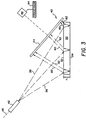
- FIG. 3 Another interferometer 40 is depicted in FIG. 3.
- Optical components of this interferometer 40 which include a point source 42, a viewing screen 44, and a camera 46, are similar to those of the interferometer 10 but are arranged much differently.
- a semiconductor wafer 50 has polished front and back side surfaces 52 and 54; but in contrast to the wafer 20, the front side surface 52 faces both the point source 42 and the viewing screen 44. Also, the wafer 50 is inclined from normal incidence to rays along an optical axis 48 of the point source 42.
- the diverging wavefront 56 is divided into two comparable wavefronts 60 and 62 by respective reflections from the front and back surfaces 52 and 54 of the wafer. Rays of the wavefront 60 reflect from the front surface 52 at respective angles of reflection equal but opposite to the angles of incidence formed by their originating rays from the diverging wavefront 56.
- Rays from the wavefront 62 refract upon entry into the wafer 50, reflect from the back surface 54, and re-refract upon exiting the wafer on paths that are parallel but laterally offset with respect to the paths of the corresponding rays of the wavefront 60.
- Both of the comparable wavefronts 60 and 62 retain substantially spherical forms, but they now appear to emanate from imaginary point sources that are relatively displaced. Since the two comparable wavefronts 60 and 62 depart from each other, a non-null interference pattern is formed on the viewing screen 44 for theoretically perfect wafers.
- the optical path length differences associated with the null condition can be calculated by a processor 64 and subtracted from the optical path length differences represented by the actual interference pattern as a measure of variations in wafer thickness "t". More exact measures of thickness variations as well as a measure of absolute thickness are obtained by modulation.
- the viewing screen 44 which functions as a diffuser, is preferably viewed by the camera 46 through light that is transmitted by the viewing screen 44.
- the camera 46 could also be positioned to view the screen 44 through light that is reflected by the screen 44.
- a fresnel lens or other focusing optic could be used in this or any of the other embodiments to collect light from the viewing screen 44 and to direct it to the camera 46.
- An interferometer 70 depicted in FIG. 4 is arranged similar to the interferometer 10 but operates in a null condition.
- a point source 72 produces a diverging spherical wavefront 86 that is reshaped into a planar wavefront 88 by a collimator 73, which can be formed by refractive, reflective, or diffractive optics.
- the planar wavefront 88 illuminates a front side surface 82 of a semiconductor wafer at normal incidence.
- the point source 72 and the collimator 73, as well as a viewing screen 74 and a camera 76, are all preferably aligned with a common optical axis 78.
- the planar wavefront 88 could also be oriented to impinge upon the front side surface 82 at a non-normal angle of incidence while preserving a null condition.
- the planar wavefront 88 is divided into two comparable wavefronts 90 and 92.
- the wavefront 90 transmits directly through the second side surface 84 to the viewing screen 74.
- the wavefront 92 reflects first from a back side surface 84 and then again from the front side surface 82 before emanating from the back side surface 84 along substantially the same path as the wavefront 90 to the viewing screen 74. Assuming that the surfaces 82 and 84 are substantially flat, the optical path length difference between the two comparable wavefronts 90 and 92 is equal to twice the thickness of the wafer 80 times the refractive index of the semiconductor material of the wafer 80.
- a processor 94 can be used to perform a conventional evaluation of the fringes appearing on the viewing screen 74 and recorded by the camera 76. Since the interfering wavefronts 90 and 92 remain substantially collimated, it would also be possible to arrange the camera 76 to view an interference pattern on the back side surface 84 of the wafer.
- FIGS. 1 and 4 The simplified interferometers of FIGS. 1 and 4 are made possible by my discovery that semiconductor wafers are both sufficiently reflective and sufficiently transmissive in the infrared spectrum to permit an interferometric comparison between a first portion of an infrared beam that is transmitted through a semiconductor wafer and a remaining portion of the infrared beam that is reflected from opposite sides of the wafer.
- C 2 I 1 • I 2 I 1 + I 2 x 100 where "I 1 " is the intensity of one of the beam portions reaching the viewing screen and "I 2 " is the intensity of the other beam portion reaching the viewing screen.
- I 1 is the intensity of one of the beam portions reaching the viewing screen
- I 2 is the intensity of the other beam portion reaching the viewing screen.
- a contrast of approximately forty percent is possible with semiconductor wafers measured in accordance with my invention.
- transmissive optical materials including optical glass do not have an index of refraction that is sufficiently different from air to maintain a beam intensity through two reflections large enough to achieve the required contrast with a portion of the same original beam that is merely transmitted.
- semiconductor materials are not transmissive. However, beginning at wavelengths near 1 ⁇ m in the infrared spectrum, semiconductor materials such as silicon become transmissive and exhibit a sufficient index of refraction to provide the required reflectivity. The precise wavelength of infrared light can be chosen to vary the sensitivity of the measurement.
- the point source 102 is similar to the point sources of the preceding embodiments, emitting a diverging beam of light 108 having a wavelength within a range at which the semiconductor wafer 106 is at least partially transmissive.
- the point source 104 emits a diverging beam 110 having a wavelength at which the semiconductor wafer 106 is substantially opaque.
- the first point source 102 can be a diode laser operating at a wavelength of 1550 nanometers
- the second point source 104 can be a HeNe laser operating at 633 nanometers.
- Collimators 112 and 114 convert the diverging beams 108 and 110 into collimated beams 116 and 118, which respectively transmit through half-wave retardation plates 120 and 122 to polarizing beamsplitters 124 and 126.
- the half-wave retardation plate 120 is adjusted with respect to the beamsplitter 124 so that substantially all of the collimated beam 116 is reflected by the beamsplitter 124 on route through a quarter-wave retardation plate 128 to a dichroic beamsplitter 130.
- the half-wave retardation plate 122 is adjusted with respect to the beamsplitter 126 to divide the collimated beam 118 into a reference beam 132 that is transmitted and a test beam 134 that is reflected.
- the reference beam 132 transmits through a quarter-wave retardation plate 136 to a reference mirror 138.
- the test beam 134 transmits through a quarter-wave retardation plate 140 to the dichroic beamsplitter 130.
- the dichroic beamsplitter 130 is wavelength sensitive for reflecting the collimated beam 116 and transmitting the collimated test beam 134.
- Both collimated beams 116 and 134 are similarly expanded by a focusing optic 142 and a collimator 144.
- the focusing optic 142 and the collimator 144 form a beam expander, which can be made either achromatic or spherochromatic with a focusing adjustment to accommodate the wavelength differences between the collimated beams 116 and 134.
- the expanded beam 116 has a wavelength that is partially transmitted and partially reflected by the semiconductor wafer 106
- the expanded test beam 134 has a wavelength that is substantially reflected by the semiconductor wafer 106.
- One portion 148 of the expanded beam 116 reflects from a front surface 150 of the wafer 106, and another portion 152 transmits through the wafer 106 and reflects from a back surface 154 of the wafer 106.
- the two beam portions 148 and 152 which have path length differences that are a function of the wafer thickness, interfere on the front surface 150 of the wafer 106 and return to the dichroic beamsplitter 130 as a first interfering beam 156.
- the quarter-wave retardation plate 128 is adjusted so the first interfering beam 156 is substantially transmitted through the beamsplitter 124.
- a focusing optic 158 forms an image of the interference pattern carried by the first interfering beam 156 on a recording surface of an infrared camera 160, and a processor 162 evaluates fringes of the interference pattern to measure thickness variations between the front and back surfaces 150 and 154 of the wafer 106.
- the expanded test beam 134 reflects from the front surface 150 of the wafer and returns to the dichroic beamsplitter 130 as a modified test beam 164 incorporating path length variations caused by irregularities in the front surface 150.
- the modified test beam 164 interferes with the reflected reference beam 132 at the beamsplitter 126 forming a second interfering beam 166 that records the path length variations undergone by the test beam 134 at the front surface 150 of the wafer 106.
- the two quarter-wave retardation plates 136 and 140 are adjusted to improve reflection and transmission efficiencies of the beamsplitter 126 for combining the reflected reference beam 132 and the modified test beam 164.
- the plates 136 and 140 also prevent light from returning to the point source 104.
- a polarizing plate 168 is adjusted to enhance contrast between the reference beam 132 and modified test beam 164 components of the second interfering beam 166.
- a focusing optic 170 forms an image of the interference pattern carried by the second interfering beam 166 on a recording surface of a CCD camera 172.
- a processor 174 which can be the same processor as the processor 162, evaluates fringes of the interference pattern to measure flatness of the wafer's front surface 150.
- a single camera sensitive to both wavelengths of the returning beams could also be used.
- the flatness of the back surface 154 can be calculated by relating both measures within a common frame of reference.
- Other configurations could also be used for simultaneously measuring flatness and thickness variations, including combinations in which flatness continues to be measured in a null condition and thickness variations are measured in a non-null condition as depicted in one of the first two embodiments.
Landscapes
- Physics & Mathematics (AREA)
- General Physics & Mathematics (AREA)
- Length Measuring Devices By Optical Means (AREA)
Claims (10)
- Procédé interférométrique pour mesurer des variations d'épaisseur de pièces de test à surfaces parallèles dans un état non-zéro, comprenant les étapes consistant à :éclairer une première de deux surfaces nominalement parallèles (22, 24) d'une pièce de test (20) avec un faisceau non collimaté (26) qui heurte la première surface parallèle (22) selon des angles d'incidence variés et qui émane d'une source de lumière (12) située d'une manière adjacente à la première surface parallèle (22) de la pièce de test (20) et qui est éloigné d'une seconde des surfaces parallèles (24) de la pièce de test (20) ;utiliser une combinaison de transmission à travers la première surface parallèle (22) et des réflexions des deux surfaces parallèles (22, 24) pour diviser le faisceau non collimaté (26) en deux faisceaux relativement modifiés (30, 32) par :la réflexion d'un des faisceaux modifiés (32) des deux surfaces parallèles (22, 24) de la pièce de test ; et la transmission des deux faisceaux relativement modifiés (30, 32) à travers les deux surfaces parallèles (22, 24) de la pièce de test (20) de telle sorte que les deux faisceaux (30, 32) émergent de la seconde surface parallèle (24) de la pièce de test (20) éloignée de la source de lumière (12) ;former un motif d'interférence entre les deux faisceaux relativement modifiés (30, 32) qui sont transmis à travers la pièce de test (20) incluant un faisceau modifié précité (32) qui réfléchit des deux surfaces parallèles (22, 24) de la pièce de test ;placer des optiques de vision (14) d'une manière adjacente à la seconde surface parallèle (24) de la pièce de test (20) et à distance de la source de lumière (12) pour observer le motif d'interférence ; et évaluer le motif d'interférence pour distinguer des variations de longueur de pas entre les deux faisceaux relativement modifiés (30, 32) pouvant être attribuées à des variations d'épaisseur, des variations de longueur des pas entre les deux faisceaux relativement modifiés (30, 32) pouvant être attribuées à des variations des angles d'incidence selon lesquels la première surface parallèle (22) de la pièce de test (20) est éclairée.
- Procédé selon la revendication 1, où ladite étape d'éclairage comprend l'éclairage de la première surface parallèle (22) de la pièce de test (20) avec un faisceau divergent (26).
- Procédé selon la revendication 2, où ladite étape d'utilisation divise le faisceau divergent (26) en deux autres faisceaux divergents (30, 32).
- Procédé selon la revendication 1, où ladite étape de placement comprend la mise en place d'un écran de vision (14) d'une manière adjacente à la seconde (24) des surfaces parallèles de la pièce de test (20) et éloigné de la source de lumière (12).
- Procédé selon la revendication 4, où ladite étape de placement comprend l'alignement de la source de lumière (12), de la pièce de test (20) et de l'écran de vision (14) le long d'un axe optique commun (18).
- Procédé selon la revendication 1, où la pièce de test (20) est une plaquette de semi-conducteur qui est sensiblement opaque à des longueurs d'ondes inférieures à 1 micromètre.
- Procédé selon la revendication 6, où le faisceau (26) émanant de la source de lumière (12) a une longueur d'ondes supérieure à 1 micromètre.
- Interféromètre (10) pour mesurer des variations d'épaisseur des pièces de test à surfaces parallèles (20) comprenant :une source de lumière (12) qui produit un faisceau de lumière divergent (26) pour éclairer une première de deux surfaces nominalement parallèles (22, 24) d'une pièce de test (20) avec le faisceau divergent (26) selon des angles d'incidence variés ;ladite source de lumière étant située d'une manière adjacente à la première surface parallèle (22) de la pièce de test (20) et éloignée d'une seconde (24) des surfaces parallèles de la pièce de test (20) ;un écran de vision (14) qui produit un motif d'interférence formé entre les première (32) et seconde (30) portions du faisceau divergent (26) qui transmet à travers les deux surfaces parallèles (22, 24) de la pièce de test (20) , la première portion de faisceau (32) étant relativement modifiée par rapport à la seconde portion de faisceau (30) par des réflexions des deux surfaces parallèles (22, 24) de la pièce de test (20) ;un processeur (34) pour évaluer le motif d'interférence pour distinguer des variations de longueur de pas entre les deux portions de faisceau relativement modifiées (30, 32) pouvant être attribuées à des variations d'épaisseur, des variations de longueur de chemin entre les deux portions de faisceau relativement modifiées (30, 32) pouvant être attribuées à des angles d'incidence variés selon lesquels la première surface de la pièce de test (20) est éclairée ;ladite pièce de test (20) étant alignée le long d'un axe optique commun (18) entre ladite source de lumière (12) et ledit écran de vision (14) ; etledit écran de vision (14) étant situé d'une manière adjacente à la seconde surface parallèle (24) de la pièce de test (20) et éloigné de ladite source de lumière (12).
- Interféromètre selon la revendication 8, où ladite source de lumière (12) produit un faisceau de lumière divergent (26) d'une longueur d'ondes supérieure à un micromètre.
- Interféromètre selon la revendication 8, où la pièce de test (20) est localisée plus près dudit écran de vision (14) que ladite source de lumière (12).
Applications Claiming Priority (3)
| Application Number | Priority Date | Filing Date | Title |
|---|---|---|---|
| US1876996P | 1996-05-31 | 1996-05-31 | |
| US18769P | 1996-05-31 | ||
| PCT/US1997/009081 WO1997045698A1 (fr) | 1996-05-31 | 1997-05-30 | Interferometre destine a la mesure des variations d'epaisseur de plaquettes de semi-conducteurs |
Publications (2)
| Publication Number | Publication Date |
|---|---|
| EP0902874A1 EP0902874A1 (fr) | 1999-03-24 |
| EP0902874B1 true EP0902874B1 (fr) | 2004-01-28 |
Family
ID=21789697
Family Applications (1)
| Application Number | Title | Priority Date | Filing Date |
|---|---|---|---|
| EP97927809A Expired - Lifetime EP0902874B1 (fr) | 1996-05-31 | 1997-05-30 | Interferometre destine a la mesure des variations d'epaisseur de plaquettes de semi-conducteurs |
Country Status (7)
| Country | Link |
|---|---|
| US (1) | US5909282A (fr) |
| EP (1) | EP0902874B1 (fr) |
| JP (1) | JP3392145B2 (fr) |
| KR (1) | KR20000016177A (fr) |
| AT (1) | ATE258675T1 (fr) |
| DE (1) | DE69727376D1 (fr) |
| WO (1) | WO1997045698A1 (fr) |
Families Citing this family (24)
| Publication number | Priority date | Publication date | Assignee | Title |
|---|---|---|---|---|
| US6381356B1 (en) * | 1996-10-23 | 2002-04-30 | Nec Corporation | Method and apparatus for inspecting high-precision patterns |
| US6366688B1 (en) * | 1998-06-13 | 2002-04-02 | Samsung Electronics Co., Ltd. | Apparatus and method for contact failure inspection in semiconductor devices |
| US6418604B1 (en) * | 1998-07-31 | 2002-07-16 | Imation Corp. | Method of fabricating die coater parts |
| US6368881B1 (en) * | 2000-02-29 | 2002-04-09 | International Business Machines Corporation | Wafer thickness control during backside grind |
| JP4080866B2 (ja) * | 2000-07-31 | 2008-04-23 | エーディーイー コーポレーション | 新校正方法を使った形状精度の改良 |
| DE10130902A1 (de) * | 2001-06-27 | 2003-01-16 | Zeiss Carl | Interferometersystem, Verfahren zum Aufnehmen eines Interferogramms und Verfahren zum Bereitstellen und Herstellen eines Objekts mit einer Soll-Oberfläche |
| US6690690B2 (en) | 2002-05-29 | 2004-02-10 | Lightgage, Inc. | Tunable laser system having an adjustable external cavity |
| AU2003258951A1 (en) * | 2002-06-24 | 2004-01-06 | Lightgage, Inc. | Multi-stage data processing for frequency-scanning interferometer |
| US7130059B2 (en) * | 2002-06-24 | 2006-10-31 | Light Gage, Inc | Common-path frequency-scanning interferometer |
| JP4216805B2 (ja) * | 2002-07-01 | 2009-01-28 | ライトゲイジ インコーポレイテッド | 非鏡面基準表面をもつ周波数走査型干渉計 |
| AU2003247725A1 (en) | 2002-07-01 | 2004-01-19 | Lightgage, Inc. | Interferometer system of compact configuration |
| JP3742801B2 (ja) * | 2003-03-18 | 2006-02-08 | 独立行政法人科学技術振興機構 | 膜厚取得方法 |
| US6847458B2 (en) * | 2003-03-20 | 2005-01-25 | Phase Shift Technology, Inc. | Method and apparatus for measuring the shape and thickness variation of polished opaque plates |
| US20050168753A1 (en) * | 2004-02-03 | 2005-08-04 | Infineon Technologies North America Corp. | Optical measurement of device features using interferometric illumination |
| WO2007044786A2 (fr) * | 2005-10-11 | 2007-04-19 | Zygo Corporation | Procédé et système d'interférométrie à décomposition spectrale |
| KR100933313B1 (ko) * | 2007-11-06 | 2009-12-22 | 한국표준과학연구원 | 웨이퍼 두께변화 측정 방법 및 장치 |
| KR100988454B1 (ko) * | 2008-01-31 | 2010-10-18 | 에스엔유 프리시젼 주식회사 | 두께 측정방법 |
| KR100942236B1 (ko) | 2008-04-08 | 2010-02-16 | 충북대학교 산학협력단 | 판유리 두께의 측정오차 보정방법 |
| EP2603790B1 (fr) | 2010-11-12 | 2016-03-30 | Ev Group E. Thallner GmbH | Équipement de mesure et procédé de mesure d'épaisseurs de couches et de défauts d'un empilement de plaquettes |
| US8687204B2 (en) * | 2011-03-24 | 2014-04-01 | Canon Kabushiki Kaisha | Method and apparatus for measuring refractive index based on a ratio between a number of second fringes divided by a difference of the number of second fringes minus a number of first fringes |
| US9341580B2 (en) | 2014-06-27 | 2016-05-17 | Applied Materials, Inc. | Linear inspection system |
| CN109001209A (zh) * | 2018-05-29 | 2018-12-14 | 宁国中辰密封件有限公司 | 一种密封条的注胶检测装置 |
| EP3896386A1 (fr) * | 2020-04-16 | 2021-10-20 | Taylor Hobson Limited | Dispositif de mesure interférométrique |
| US20250012560A1 (en) * | 2023-07-07 | 2025-01-09 | Applied Materials, Inc. | Sample thickness metrology using focused beam interference |
Family Cites Families (21)
| Publication number | Priority date | Publication date | Assignee | Title |
|---|---|---|---|---|
| US2518647A (en) * | 1948-01-07 | 1950-08-15 | Celanese Corp | Interferometer means for thickness measurements |
| US3735036A (en) * | 1970-10-26 | 1973-05-22 | Express I M Co | Real time interferometry contour mapping system |
| DE2758149C2 (de) * | 1977-12-27 | 1979-10-04 | Ibm Deutschland Gmbh, 7000 Stuttgart | Interferometrisches Verfahren mit λ /4-Auflösung zur Abstands-, Dicken- und/oder Ebenheitsmessung |
| JPS5535214A (en) * | 1978-09-04 | 1980-03-12 | Asahi Chem Ind Co Ltd | Method and device for film-thickness measurement making use of infrared-ray interference |
| DE3048558A1 (de) * | 1980-12-22 | 1982-07-22 | Battelle-Institut E.V., 6000 Frankfurt | Verfahren und vorrichtung zur beruehrungslosen vermessung von kontaktlinsen |
| US4606638A (en) * | 1983-11-03 | 1986-08-19 | Zygo Corporation | Distance measuring interferometer and method of use |
| EP0179935B1 (fr) * | 1984-10-31 | 1988-05-18 | Ibm Deutschland Gmbh | Analyseur interférométrique de l'épaisseur et méthode de mesure |
| DD265055A3 (de) * | 1986-07-29 | 1989-02-22 | Technisches Glas Veb K | Anordnung zur interferometrischen abstands- und dickenmessung |
| JPS63222207A (ja) * | 1987-03-11 | 1988-09-16 | Japan Spectroscopic Co | 凹部深さ・膜厚測定装置 |
| SU1747877A1 (ru) * | 1990-02-28 | 1992-07-15 | Северо-Западный Заочный Политехнический Институт | Интерференционный способ измерени толщины полупроводниковых слоев |
| US5333049A (en) * | 1991-12-06 | 1994-07-26 | Hughes Aircraft Company | Apparatus and method for interferometrically measuring the thickness of thin films using full aperture irradiation |
| US5386119A (en) * | 1993-03-25 | 1995-01-31 | Hughes Aircraft Company | Apparatus and method for thick wafer measurement |
| JP3234353B2 (ja) * | 1993-06-15 | 2001-12-04 | 富士写真フイルム株式会社 | 断層情報読取装置 |
| JPH074922A (ja) * | 1993-06-21 | 1995-01-10 | Jasco Corp | 半導体多層薄膜膜厚測定装置およびその測定方法 |
| US5555472A (en) * | 1993-12-22 | 1996-09-10 | Integrated Process Equipment Corp. | Method and apparatus for measuring film thickness in multilayer thin film stack by comparison to a reference library of theoretical signatures |
| US5471303A (en) * | 1994-04-29 | 1995-11-28 | Wyko Corporation | Combination of white-light scanning and phase-shifting interferometry for surface profile measurements |
| US5513553A (en) * | 1994-07-13 | 1996-05-07 | Gleasman; Vernon E. | Hydraulic machine with gear-mounted swash-plate |
| US5515167A (en) * | 1994-09-13 | 1996-05-07 | Hughes Aircraft Company | Transparent optical chuck incorporating optical monitoring |
| US5502564A (en) * | 1994-09-13 | 1996-03-26 | Hughes Aircraft Company | Substrate thickness measurement using oblique incidence multispectral interferometry |
| US5596409A (en) * | 1995-03-22 | 1997-01-21 | Eastman Kodak Company | Associated dual interferometric measurement method for determining a physical property of an object |
| US5555471A (en) * | 1995-05-24 | 1996-09-10 | Wyko Corporation | Method for measuring thin-film thickness and step height on the surface of thin-film/substrate test samples by phase-shifting interferometry |
-
1997
- 1997-05-30 DE DE69727376T patent/DE69727376D1/de not_active Expired - Lifetime
- 1997-05-30 JP JP54291297A patent/JP3392145B2/ja not_active Expired - Fee Related
- 1997-05-30 WO PCT/US1997/009081 patent/WO1997045698A1/fr not_active Ceased
- 1997-05-30 US US08/866,540 patent/US5909282A/en not_active Expired - Fee Related
- 1997-05-30 KR KR1019980709745A patent/KR20000016177A/ko not_active Withdrawn
- 1997-05-30 EP EP97927809A patent/EP0902874B1/fr not_active Expired - Lifetime
- 1997-05-30 AT AT97927809T patent/ATE258675T1/de not_active IP Right Cessation
Also Published As
| Publication number | Publication date |
|---|---|
| WO1997045698A1 (fr) | 1997-12-04 |
| EP0902874A1 (fr) | 1999-03-24 |
| ATE258675T1 (de) | 2004-02-15 |
| DE69727376D1 (de) | 2004-03-04 |
| US5909282A (en) | 1999-06-01 |
| KR20000016177A (ko) | 2000-03-25 |
| JP2000501508A (ja) | 2000-02-08 |
| JP3392145B2 (ja) | 2003-03-31 |
Similar Documents
| Publication | Publication Date | Title |
|---|---|---|
| EP0902874B1 (fr) | Interferometre destine a la mesure des variations d'epaisseur de plaquettes de semi-conducteurs | |
| US4872755A (en) | Interferometer for measuring optical phase differences | |
| KR101232204B1 (ko) | 등경로 간섭계 | |
| US6249351B1 (en) | Grazing incidence interferometer and method | |
| JP2997047B2 (ja) | 光学式計測装置 | |
| JP4223349B2 (ja) | 耐振動型干渉計装置 | |
| WO2003067182A1 (fr) | Procede de mesure d'interference differentielle et interferometre differentiel, procede de production d'un systeme optique de projection, systeme optique de projection, et systeme d'exposition par projection | |
| US7538890B2 (en) | Wavefront-measuring interferometer apparatus, and light beam measurement apparatus and method thereof | |
| US4105335A (en) | Interferometric optical phase discrimination apparatus | |
| US6590654B1 (en) | Polarized illumination and detection for metrological applications | |
| CN114577111A (zh) | 面形检测系统及检测方法 | |
| JP2006343121A (ja) | 光ビーム測定装置 | |
| JPH08334606A (ja) | レンズ | |
| JP2000088513A (ja) | 非球面波発生レンズ系組立調整装置 | |
| JPH05500853A (ja) | ガラス管壁の厚さを決定するための方法及び装置 | |
| JP3461566B2 (ja) | 円錐形状測定用干渉計 | |
| JP3010085B2 (ja) | ホログラム干渉計 | |
| CN109764963A (zh) | 一种棱镜型空间外差光谱仪基准波长设置及调试方法 | |
| JP2966950B2 (ja) | 試料変位測定装置 | |
| JPH0611308A (ja) | ホログラム干渉計 | |
| GB2333834A (en) | Interferometer with deadpath error compensation | |
| JPH11325848A (ja) | 非球面形状測定装置 | |
| JPH02259512A (ja) | 一体型干渉測定装置 | |
| SU1728650A1 (ru) | Интерферометр дл контрол вогнутых асферических поверхностей | |
| SU1762116A1 (ru) | Дифракционный интерферометр |
Legal Events
| Date | Code | Title | Description |
|---|---|---|---|
| PUAI | Public reference made under article 153(3) epc to a published international application that has entered the european phase |
Free format text: ORIGINAL CODE: 0009012 |
|
| 17P | Request for examination filed |
Effective date: 19981221 |
|
| AK | Designated contracting states |
Kind code of ref document: A1 Designated state(s): AT BE CH DE FR GB IE IT LI SE |
|
| 17Q | First examination report despatched |
Effective date: 20020729 |
|
| GRAP | Despatch of communication of intention to grant a patent |
Free format text: ORIGINAL CODE: EPIDOSNIGR1 |
|
| GRAS | Grant fee paid |
Free format text: ORIGINAL CODE: EPIDOSNIGR3 |
|
| GRAA | (expected) grant |
Free format text: ORIGINAL CODE: 0009210 |
|
| AK | Designated contracting states |
Kind code of ref document: B1 Designated state(s): AT BE CH DE FR GB IE IT LI SE |
|
| PG25 | Lapsed in a contracting state [announced via postgrant information from national office to epo] |
Ref country code: LI Free format text: LAPSE BECAUSE OF FAILURE TO SUBMIT A TRANSLATION OF THE DESCRIPTION OR TO PAY THE FEE WITHIN THE PRESCRIBED TIME-LIMIT Effective date: 20040128 Ref country code: IT Free format text: LAPSE BECAUSE OF FAILURE TO SUBMIT A TRANSLATION OF THE DESCRIPTION OR TO PAY THE FEE WITHIN THE PRESCRIBED TIME-LIMIT;WARNING: LAPSES OF ITALIAN PATENTS WITH EFFECTIVE DATE BEFORE 2007 MAY HAVE OCCURRED AT ANY TIME BEFORE 2007. THE CORRECT EFFECTIVE DATE MAY BE DIFFERENT FROM THE ONE RECORDED. Effective date: 20040128 Ref country code: FR Free format text: LAPSE BECAUSE OF FAILURE TO SUBMIT A TRANSLATION OF THE DESCRIPTION OR TO PAY THE FEE WITHIN THE PRESCRIBED TIME-LIMIT Effective date: 20040128 Ref country code: CH Free format text: LAPSE BECAUSE OF FAILURE TO SUBMIT A TRANSLATION OF THE DESCRIPTION OR TO PAY THE FEE WITHIN THE PRESCRIBED TIME-LIMIT Effective date: 20040128 Ref country code: BE Free format text: LAPSE BECAUSE OF FAILURE TO SUBMIT A TRANSLATION OF THE DESCRIPTION OR TO PAY THE FEE WITHIN THE PRESCRIBED TIME-LIMIT Effective date: 20040128 Ref country code: AT Free format text: LAPSE BECAUSE OF FAILURE TO SUBMIT A TRANSLATION OF THE DESCRIPTION OR TO PAY THE FEE WITHIN THE PRESCRIBED TIME-LIMIT Effective date: 20040128 |
|
| REG | Reference to a national code |
Ref country code: GB Ref legal event code: FG4D |
|
| REG | Reference to a national code |
Ref country code: CH Ref legal event code: EP |
|
| REG | Reference to a national code |
Ref country code: IE Ref legal event code: FG4D |
|
| REF | Corresponds to: |
Ref document number: 69727376 Country of ref document: DE Date of ref document: 20040304 Kind code of ref document: P |
|
| PG25 | Lapsed in a contracting state [announced via postgrant information from national office to epo] |
Ref country code: SE Free format text: LAPSE BECAUSE OF FAILURE TO SUBMIT A TRANSLATION OF THE DESCRIPTION OR TO PAY THE FEE WITHIN THE PRESCRIBED TIME-LIMIT Effective date: 20040428 |
|
| PG25 | Lapsed in a contracting state [announced via postgrant information from national office to epo] |
Ref country code: DE Free format text: LAPSE BECAUSE OF FAILURE TO SUBMIT A TRANSLATION OF THE DESCRIPTION OR TO PAY THE FEE WITHIN THE PRESCRIBED TIME-LIMIT Effective date: 20040429 |
|
| PG25 | Lapsed in a contracting state [announced via postgrant information from national office to epo] |
Ref country code: IE Free format text: LAPSE BECAUSE OF NON-PAYMENT OF DUE FEES Effective date: 20040531 |
|
| PGFP | Annual fee paid to national office [announced via postgrant information from national office to epo] |
Ref country code: GB Payment date: 20040623 Year of fee payment: 8 |
|
| REG | Reference to a national code |
Ref country code: CH Ref legal event code: PL |
|
| PLBE | No opposition filed within time limit |
Free format text: ORIGINAL CODE: 0009261 |
|
| STAA | Information on the status of an ep patent application or granted ep patent |
Free format text: STATUS: NO OPPOSITION FILED WITHIN TIME LIMIT |
|
| 26N | No opposition filed |
Effective date: 20041029 |
|
| EN | Fr: translation not filed | ||
| REG | Reference to a national code |
Ref country code: IE Ref legal event code: MM4A |
|
| PG25 | Lapsed in a contracting state [announced via postgrant information from national office to epo] |
Ref country code: GB Free format text: LAPSE BECAUSE OF NON-PAYMENT OF DUE FEES Effective date: 20050530 |
|
| GBPC | Gb: european patent ceased through non-payment of renewal fee |
Effective date: 20050530 |