EP0899683A2 - Chipkarte mit Gebrauchsanzeige und Anordnung dafür - Google Patents
Chipkarte mit Gebrauchsanzeige und Anordnung dafür Download PDFInfo
- Publication number
- EP0899683A2 EP0899683A2 EP98402122A EP98402122A EP0899683A2 EP 0899683 A2 EP0899683 A2 EP 0899683A2 EP 98402122 A EP98402122 A EP 98402122A EP 98402122 A EP98402122 A EP 98402122A EP 0899683 A2 EP0899683 A2 EP 0899683A2
- Authority
- EP
- European Patent Office
- Prior art keywords
- card
- writer
- state
- short
- usage
- Prior art date
- Legal status (The legal status is an assumption and is not a legal conclusion. Google has not performed a legal analysis and makes no representation as to the accuracy of the status listed.)
- Granted
Links
Images


Classifications
-
- G—PHYSICS
- G06—COMPUTING OR CALCULATING; COUNTING
- G06K—GRAPHICAL DATA READING; PRESENTATION OF DATA; RECORD CARRIERS; HANDLING RECORD CARRIERS
- G06K19/00—Record carriers for use with machines and with at least a part designed to carry digital markings
- G06K19/06—Record carriers for use with machines and with at least a part designed to carry digital markings characterised by the kind of the digital marking, e.g. shape, nature, code
- G06K19/067—Record carriers with conductive marks, printed circuits or semiconductor circuit elements, e.g. credit or identity cards also with resonating or responding marks without active components
- G06K19/07—Record carriers with conductive marks, printed circuits or semiconductor circuit elements, e.g. credit or identity cards also with resonating or responding marks without active components with integrated circuit chips
- G06K19/077—Constructional details, e.g. mounting of circuits in the carrier
- G06K19/0772—Physical layout of the record carrier
- G06K19/07726—Physical layout of the record carrier the record comprising means for indicating first use, e.g. a frangible layer
-
- G—PHYSICS
- G06—COMPUTING OR CALCULATING; COUNTING
- G06K—GRAPHICAL DATA READING; PRESENTATION OF DATA; RECORD CARRIERS; HANDLING RECORD CARRIERS
- G06K19/00—Record carriers for use with machines and with at least a part designed to carry digital markings
- G06K19/06—Record carriers for use with machines and with at least a part designed to carry digital markings characterised by the kind of the digital marking, e.g. shape, nature, code
- G06K19/067—Record carriers with conductive marks, printed circuits or semiconductor circuit elements, e.g. credit or identity cards also with resonating or responding marks without active components
- G06K19/07—Record carriers with conductive marks, printed circuits or semiconductor circuit elements, e.g. credit or identity cards also with resonating or responding marks without active components with integrated circuit chips
- G06K19/077—Constructional details, e.g. mounting of circuits in the carrier
- G06K19/07749—Constructional details, e.g. mounting of circuits in the carrier the record carrier being capable of non-contact communication, e.g. constructional details of the antenna of a non-contact smart card
- G06K19/07773—Antenna details
- G06K19/07777—Antenna details the antenna being of the inductive type
- G06K19/07779—Antenna details the antenna being of the inductive type the inductive antenna being a coil
- G06K19/07783—Antenna details the antenna being of the inductive type the inductive antenna being a coil the coil being planar
-
- G—PHYSICS
- G06—COMPUTING OR CALCULATING; COUNTING
- G06K—GRAPHICAL DATA READING; PRESENTATION OF DATA; RECORD CARRIERS; HANDLING RECORD CARRIERS
- G06K19/00—Record carriers for use with machines and with at least a part designed to carry digital markings
- G06K19/06—Record carriers for use with machines and with at least a part designed to carry digital markings characterised by the kind of the digital marking, e.g. shape, nature, code
- G06K19/067—Record carriers with conductive marks, printed circuits or semiconductor circuit elements, e.g. credit or identity cards also with resonating or responding marks without active components
- G06K19/07—Record carriers with conductive marks, printed circuits or semiconductor circuit elements, e.g. credit or identity cards also with resonating or responding marks without active components with integrated circuit chips
- G06K19/077—Constructional details, e.g. mounting of circuits in the carrier
- G06K19/07749—Constructional details, e.g. mounting of circuits in the carrier the record carrier being capable of non-contact communication, e.g. constructional details of the antenna of a non-contact smart card
- G06K19/07773—Antenna details
- G06K19/07777—Antenna details the antenna being of the inductive type
- G06K19/07784—Antenna details the antenna being of the inductive type the inductive antenna consisting of a plurality of coils stacked on top of one another
-
- H—ELECTRICITY
- H05—ELECTRIC TECHNIQUES NOT OTHERWISE PROVIDED FOR
- H05K—PRINTED CIRCUITS; CASINGS OR CONSTRUCTIONAL DETAILS OF ELECTRIC APPARATUS; MANUFACTURE OF ASSEMBLAGES OF ELECTRICAL COMPONENTS
- H05K1/00—Printed circuits
- H05K1/02—Details
- H05K1/0286—Programmable, customizable or modifiable circuits
Definitions
- the present invention relates to an IC card which is fed electricity by an IC card reader-writer via electromagnetic or electrostatic coupling (that is, power is supplied from the IC card reader-writer to the IC card), and between these IC card and IC card reader-writer, data transmission is performed.
- the present invention relates to an IC card having a function of indicating its state of usage and a system therefor, and a method for indicating a state of usage.
- figures and punch holes are provided for indicating whether the card has already been used, or how much the card has been used.
- figures indicating charges and corresponding degrees of use are previously indicated from a lower limit to an upper limit, and by punching a hole near each figure, the present state of usage is shown to a user.
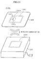
- Fig. 11 is a perspective view showing electromagnetic coupling type contactless IC card C100.
- the IC card C100 comprises card substrate 100B, coil 100C for electromagnetic coupling, IC chip 100CH, and outside terminals (or pads) 100T 1 and 100T 2 for the IC chip.
- a PVC (polyvinyl chloride) resin, an ABS resin, or a PET (polyethylene terephthalate) resin may be used for making card substrate 100B.
- the IC chip 100CH and electromagnetic coupling coil 100C which are connected to each other via outside terminals 100T 1 and 100T 2 , are arranged inside the card substrate 100B or are put between two portions of the substrate.
- the contactless IC card C100 is electromagnetically coupled with IC card reader-writer 200 having electromagnetic coupling coil 200C, and thereby the IC card and the reader-writer are wirelessly communicated with each other.
- the IC card reader-writer 200 comprises the electromagnetic coupling coil 200C which is electromagnetically coupled with coil 100C of IC card C100.
- the thickness of conventional contact and contactless IC cards is larger than that of magnetic cards; thus, it is difficult to punch a hole and indicate a state of usage as in the case of a magnetic prepaid card.
- a function of punching a hole is provided in public telephones, construction of the public telephone becomes complicated and thus trouble may be caused.
- the contactless IC card C100 wirelessly communicates with an external device including IC card reader-writer 200, the contactless IC card C100 is not attached to the above external device; thus, it is impossible to record, in a specified or predetermined area on a surface of the card, a state of usage of the card by, for example, punching a hole, as in the case of a magnetic prepaid card.
- an object of the present invention is to provide an IC card whose state of usage can be judged by a user from an appearance of the card, a relevant IC card system, and a method for indicating a state of usage of an IC card.
- the present invention provides an IC card fed electricity from an IC card reader-writer via feeding means using one of electromagnetic coupling and electrostatic coupling, and the IC card having an IC chip which communicates with the IC card reader-writer, wherein the possible/impossible state of usage of the card by a user is determined using electric means for disconnecting or non-disconnecting the feeding means or providing another circuit and disconnecting this circuit, and the appearance of the IC card is also changed at the time of the change caused by such electric means and thereby the state of usage of the card is indicated to the user.
- the IC card may have a notch and a portion of the conductor is exposed at the notch, and the short-circuited state may be freed by cutting the exposed conductor.
- the IC card may have a notch and a portion of the means for generating the current having the reversed polarity is exposed at the notch, and the current of the reversed polarity may be disconnected by cutting the exposed portion of said means.
- the IC card may comprise indicating means for indicating information relating to a state of usage of the IC card.
- indicating means can be easily realized using a fuse or a thermochromic material.
- a plurality of the fuses or thermochromic materials may be provided, and thereby it is possible to indicate whether the card reaches each of predetermined degrees of use.
- the present invention also provides an IC card system comprising an IC card which has any of the above-described features and an IC card reader-writer.
- the present invention further provides a method of indicating a state of usage of an IC card having a corresponding feature.
- the user who obtains the IC card can easily and surely confirm that the IC card has not yet been used before the user suitably starts to use the card. It is also possible for the user to obtain information relating to a state of usage of the card in use.
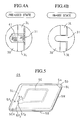
- Fig. 1 is a perspective view of contactless IC card C1 of the first embodiment according to the present invention.
- Fig. 2 is a perspective view of contactless IC card C2 of the second embodiment according to the present invention.
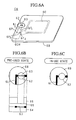
- Fig. 3A is a perspective view of contactless IC card C3 of the third embodiment according to the present invention
- Figs. 3B and 3C are enlarged views of notch 31 area of the card C3 in the pre-used and in-use states.
- Figs. 4A and 4B are enlarged views of notch 31 area of the card C4 in the pre-used and in-use states.
- Fig. 5 is a perspective view of contactless IC card C5 of the fifth embodiment according to the present invention.
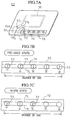
- Fig. 6A is a perspective view of contactless IC card C6 of the sixth embodiment according to the present invention
- Figs. 6B and 6C are diagrams showing usage state indicator 62 of the card C6 in the pre-used and in-use states.
- Fig. 7A is a perspective view of contactless IC card C7 of the seventh embodiment according to the present invention
- Figs. 7B and 7C are diagrams showing usage state indicator 72 of the card C7 in the pre-used and in-use states.
- Fig. 8A is a perspective view of contactless IC card C8 of the eighth embodiment according to the present invention
- Figs. 8B and 8C are diagrams showing usage state indicator 82 of the card C8 in the pre-used and in-use states.
- Fig. 9A is a perspective view of contactless IC card C9 of the ninth embodiment according to the present invention
- Figs. 9B and 9C are diagrams showing usage state indicator 92 of the card C9 in the pre-used and in-use states.
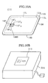
- Fig. 10A is a perspective view of contact IC card C10 of the tenth embodiment according to the present invention
- Fig. 10B shows the structure of IC card reader-writer 300 for communicating with the contact IC card C10.
- Fig. 11 is a perspective view showing electromagnetic coupling type contactless IC card C100 as a conventional example.
- Fig. 1 is a perspective view of contactless IC card C1 of the first embodiment according to the present invention.
- the contactless IC card C1 comprising card substrate 1B is composed of main body 1M and separable portion 1D.
- the main body 1M comprises electromagnetic coupling coil 1C, IC chip 1CH, and outside terminals 1T 1 and 1T 2 , etc.
- the separable portion 1D has a portion of line 1S for short-circuiting electromagnetic coupling coil 1C.
- the short-circuiting line 1S is connected with electromagnetic coupling coil 1C and connected to outside terminals 1T 1 and 1T 2 of IC chip 1CH so as to short-circuit electromagnetic coupling coil 1C. Between the main body 1M and separable portion 1D, perforation 1m is provided. By bending or twisting the IC card C1 with respect to the perforation 1m as a boundary, it is possible to separate the separable portion 1D from the main body 1M. According to this separation, short-circuiting line 1S is cut at perforation 1m as the boundary, and the line is opened.
- the main body 1M and the separable portion 1D should be separated from each other. According to this separation, the short-circuiting line 1S is opened, and thereby when the card receives an electromagnetic wave from the IC card reader-writer, current caused by the electromagnetic induction flows in IC chip 1CH and the chip is fed electricity. Communication between the card and the reader-writer then becomes possible.
- the general formation of the IC card including separable portion 1D in Fig. 1 conforms to the standard ISO/IEC 7810 1D-1.
- the main body 1M may conform to the above standard ISO/IEC 7810 1D-1 and separable portion 1D may be provided as a projecting portion.
- the above short-circuiting line 1S may be a lead wire or a pattern using a copper foil or a silver paste. Such a variation is also possible for the second embodiment explained below.
- the user may divide the two portions using hands, or a device like a blade cutter equipped in a cutter may be provided in an external device which includes an IC card reader-writer like reader-writer 200 as shown in Fig. 11, in a vending machine of contactless IC cards, or in a collection box for used contactless IC cards, so as to separate the portion 1D from the card.
- a device like a blade cutter equipped in a cutter may be provided in an external device which includes an IC card reader-writer like reader-writer 200 as shown in Fig. 11, in a vending machine of contactless IC cards, or in a collection box for used contactless IC cards, so as to separate the portion 1D from the card.
- Fig. 2 is a perspective view of contactless IC card C2 of the second embodiment according to the present invention.
- the contactless IC card C2 comprising card substrate 2B is composed of main body 2M and separable portion 2D.
- the main body 2M comprises electromagnetic coupling coils 2C 1 and 2C 2 , IC chip 2CH, outside terminals 2T 1 and 2T 2 .
- the separable portion 2D has a portion of electromagnetic coupling coil 2C 2 .
- the electromagnetic coupling coils 2C 1 and 2C 2 have the same size and the same number of winding rounds, and the coils are respectively wound in reverse directions. Between the main body 2M and separable portion 2D, perforation 2m is provided. By bending or twisting the IC card C2 with respect to the perforation 2m as a boundary, it is possible to separate the separable portion 2D from the main body 2M. According to this separation, electromagnetic coupling coil 2C 2 is cut at perforation 1m as the boundary, and the coil is opened.
- the main body 2M and the separable portion 2D should be separated from each other. According to this separation, the electromagnetic coupling coil 2C 2 is opened and the signal from this coil cannot be transmitted.
- a pre-used contactless IC card C2 can be safely handed over from an issuer to a user, and possible fraudulent usage before proper use by the user can be prevented.
- the electromagnetic coupling coils 2C 1 and 2C 2 can be formed using the same coil (material) and thus the cost can be reduced.
- Fig. 3A is a perspective view of contactless IC card C3 of the third embodiment according to the present invention.
- the contactless IC card C3 comprises card substrate 3B, electromagnetic coupling coil 3C, IC chip 3CH, outside terminals 3T 1 and 3T 2 , lead wire 3L having a rounded-square shape, lead wire connecting terminals (or pads) 3P 1 and 3P 2 , and U-shaped notch 31.
- a user can cut lead wire 3L by, for example, hooking the wire at the user's nail, and thereby the user can start to use this IC card (refer to Fig. 3C).
- the contactless IC card C3 even in a pre-used state, that is, in a state in which the lead wire 3L has not yet been cut, electromagnetic coupling coil 3C is not short-circuited; thus, communication with the IC card reader-writer is possible.
- an initial anti-collision operation using the IC card reader-writer an initial response request is sent to the contactless IC card C3, and the IC card C3 returns information relating to a protocol to be used, the kind of the IC card, and a possible degree of use, as a response.
- IC chip 3CH checks whether the lead wire connecting terminals 3P 1 and 3P 2 are connected with each other, by, for example, applying a voltage to lead wire connecting terminal 3P 1 .
- the contactless IC card C3 if the contactless IC card C3 has not yet been used, current is generated around the rounded-square shaped lead wire 3L by applying voltage to the lead wire connecting terminal. Therefore, by detecting the current, the IC chip CH3 can recognize that the contactless IC card C3 has not yet been used. The contactless IC card C3 then sends the IC card reader-writer 200 information indicating that the IC card C3 has not yet been used, as an initial response.
- the state that the contactless IC card C3 has not yet been used is shown in a display (such as an LCD display) of an external device which includes the IC card reader-writer 200.
- the contactless IC card C3 After sending the information indicating a pre-used state, the contactless IC card C3 does not communicate with the IC card reader-writer. Therefore, the user can recognize that it is impossible to use the IC card in the present state and understand the necessity of cutting lead wire 3L so as to start to use the card.
- restricted communication may be continued after sending the information indicating a pre-used state. That is, information relating to functions other than the subtraction of the degree of use, such as a "telephone directory" function, may be communicated and be operable.
- IC card C3 in a first state in which lead wire connecting terminals 3P 1 and 3P 2 are connected with each other via lead wire 3L, IC card C3 can perform only restricted communication (that is, communication relating to functions to be previously performed before ordinary usage) with IC card reader-writer 200.
- the contactless IC card C3 is used as a phone card, it is possible to display the degree of use, for example, "50” (units) and a message like "PLEASE MAKE THE CARD POSSIBLE TO USE", so as to advise the user to start to use the card.
- a lead wire cutting device having a projecting portion or the like may be attached to an external device including IC card reader-writer 200 (as shown in Fig. 11), to a contactless IC card vending machine, or to a collection box for used contactless IC cards.
- lead wire 3L can be cut by hooking the wire on the cutting device.
- contactless IC card C3 Before the contactless IC card C3 sends an initial response to IC card reader-writer 200, it is possible for contactless IC card C3 itself to check the possible degree of use recorded and stored in IC chip 3CH and judge whether the checked degree corresponds to a pre-used state, and only in the case in which the degree indicates the pre-used state, contactless IC card C3 may detect the state of the lead wire connecting terminals, by its own processing.
- detection of the state of the lead wire connecting terminals is performed with reference to the degree of use.
- a starting flag is used and is set to be in an "on" state when the usage is started, and that the state of the usage of the card is judged according to the state of this flag.
- the contactless IC card C3 sends internal information as an initial response to an external device including IC card reader-writer 200, the external device may send the contactless IC card C3 a request for checking the state of the lead wire connecting terminals 3P 1 and 3P 2 , and the above judgment operation is performed according to a response to the request.
- contactless IC card C4 as the fourth embodiment of the present invention will be explained.
- the basic structure of the contactless IC card C4 is the same as the above explained contactless IC card C3.
- Fig. 4A is an enlarged view of the U-shaped notch 31 in the contactless IC card C4.
- the contactless IC card C4 is the same as the contactless IC card C3 except that seal 41 for protecting the IC card C4 is provided.
- contactless IC card C4 corresponds to contactless IC card C3 with protection seal 41.
- the protection seal 41 is peeled from the contactless IC card C4 and lead wire 3L is cut, the contactless IC card C4 is just the same as the contactless IC card C3, as shown in Fig. 4B.
- the protection seal 41 is provided for preventing the lead wire 3L, which is exposed at notch 31, from breaking during transportation of the card, or the like.
- the protection seal 41 and the lead wire 3L may be stuck to each other so as to automatically cut the wire at the time of peeling the seal. In this case, the user's operation of cutting the lead wire, performed after peeling the protection seal 41, can be saved.
- the above-explained structure having a notch may be applied to the second embodiment. That is, a portion of electromagnetic coupling coil 2C 2 in Fig. 2 is exposed at a notch like notch 31 and the exposed portion is cut so as to make the card usable.
- Fig. 5 is a perspective view of contactless IC card C5 of the fifth embodiment according to the present invention.
- the contactless IC card C5 comprising card substrate 5B is composed of main body 5M and separable portion 5D.
- the main body 5M comprises electromagnetic coupling coil 5C, IC chip 5CH, outside terminals 5T 1 and 5T 2 , lead wire 5L having a rounded-square shape, and lead wire connecting terminals 5P 1 and 5P 2 .
- the separable portion 5D includes a portion of lead wire 5L. Between the main body 5M and separable portion 5D, perforation 5m is provided. By bending or twisting the contactless IC card C5 with respect to the perforation 5m as a boundary, it is possible to separate the separable portion 5D from the main body 5M. According to this separation, lead wire 5L is cut at perforation 5m as the boundary, and the lead wire connecting terminals 5P 1 and 5P 2 are opened.
- the contactless IC card C5 As in the third (or fourth) embodiment, even in a pre-used state in which main body 5M and separable portion 5D has not yet been separated, electromagnetic coupling coil 5C is not short-circuited; thus, communication with the IC card reader-writer is possible in this state. Therefore, as in the third embodiment, when an initial response request is sent from the IC card reader-writer to contactless IC card C5, the IC card C5 can return information relating to a protocol to be used, the kind of the IC card, and the degree of use, as a response. In this operation, IC chip CH5 checks whether the lead wire connecting terminals 5P 1 and 5P 2 are connected with each other by, for example, applying a voltage to lead wire connecting terminal 5P 1 .
- the contactless IC card C5 In a pre-used state of the contactless IC card, the main body 5M and the separable portion 5D are not separated and main portions of the lead wire 5L included in the main body 5M and the remaining portion of lead wire 5L included in the separable portion 5D are connected with each other. Therefore, if voltage is applied to the lead wire connecting terminal, then current is generated around the roundedsquared lead wire 5L.
- the following operations are similar to those performed in the third embodiment. That is, after sending information relating to the pre-used state, the contactless IC card C5 does not perform communication with the IC card reader-writer. Therefore, the user recognizes that the contactless IC card C5 cannot be used in the present state and understands the necessity of separating the separable portion 5D from the main body 5M so as to use the card.
- the separable portion 5D is separated from the main body 5M and IC chip 5CH detects the state of lead wire connecting terminals 5P 1 and 5P 2 by applying voltage to the lead wire connecting terminal, then no current flows in lead wire 5L and the IC chip 5CH recognizes that the contactless IC card C5 is in use.
- the chip 5CH performs the following communication.
- contactless IC card C5 before the contactless IC card C5 sends an initial response to IC card reader-writer 200, it is possible for contactless IC card C5 itself to check the possible degree of use recorded and stored in IC chip 5CH and judge whether the degree corresponds to a pre-used state, and only in the case in which the degree indicates the pre-used state, contactless IC card C5 may detect the state of the lead wire connecting terminals, of its own initiative.
- the contactless IC card C5 instead of providing the function of detecting "whether the lead wire is cut" to the contactless IC card C5 itself, the following operation is possible in which when the contactless IC card C5 sends internal information as an initial response to an external device including IC card reader-writer 200, the external device may send the contactless IC card C5 a request for checking the state of the lead wire connecting terminals 5p 1 and 5P 2 , and the above judgment operation is performed according to a response to the request.
- a core sheet in which an IC chip and an antenna like an electromagnetic coupling coil are mounted is made, (ii) an IC card is made by putting the core sheet between over sheets, and (iii) necessary information is written (or encoded) via wireless communication. That is, in the processes from manufacturing to issuance, the encoding operation can be performed for a finished IC card as shown in Fig. 5. In this case, manufacturing costs can be reduced.
- IC chip 5CH is mounted at the opposite corner on a diagonal line with respect to perforation 5m.
- the IC chip 5CH can be protected from a stress or impact imposed when a user separates the separable portion 5M from the main body 5D.
- test pads used in a screening process of chips (such as the burn-in process) performed in the manufacturing of IC chips 5CH may be used as lead wire connecting terminals 5P 1 and 5P 2 .
- a countermeasure for blocking unfair access to the IC chip 5CH from the cut portion at the perforation 5m must be taken in the IC chip 5CH.
- Fig. 6A is a perspective view of contactless IC card C6 of the sixth embodiment according to the present invention.
- the contactless IC card C6 comprises card substrate 6B, electromagnetic coupling coil 6C, IC chip 6CH, outside terminals 6T 1 and 6T 2 , lead wires 6L, lead wire connecting terminals 6P 1 and 6P 2 , indicator 62 for indicating the state of usage, and fuse 63.
- the bold circle in Fig. 6A corresponds to enlarged views in Figs. 6B and 6C.
- fuse 63 is not fused, and once the contactless IC card C6 is used, then the fuse 63 is fused by IC chip 6CH.
- fuse 63 exists in usage state indicator 62, and is connected to lead wires 6L in the neighborhood of the indicator 62.
- the lead wires 6L are connected to IC chip 6CH via lead wire connecting terminals 6P 1 and 6P 2 which are independent of outside terminals 6T 1 and 6T 2 .
- the user can confirm whether or not the fuse 63 is fused by peeping into the usage state indicator 62 from the surface side of the card.
- a design indicated by the user may be printed on the surface of the card C6; thus, it is preferable that usage state indicator 62 be provided on the back face of the card.
- a circular hole is provided in over sheet 64 on the back face of the card and the state of fuse 63 can be observed through transparent core sheet 65 (from above the core sheet).
- the fuse 63 can be protected from the outside. If fuse 63 is positioned on the core sheet 65, this area should be covered with a transparent protection sheet.
- electromagnetic coupling coil 6C is not short-circuited; thus, communication with IC card reader-writer 200 is possible even though the contactless IC card C6 has not yet been used.
- the card C6 checks whether the two lead wire connecting terminals 6P 1 and 6P 2 are connected with each other by, for example, applying a voltage to the lead wire connecting terminals, before returning an initial response with respect to an initial response request sent from the IC card reader-writer 200.
- a voltage which cannot disconnect fuse 63 is applied between the lead wire connecting terminals 6P 1 and 6P 2 ; thus, current flows while fuse 63 is not disconnected and the two lead wires 6L are connected with each other via the fuse.
- the IC chip 6CH recognizes that the contactless IC card C6 has not yet been used.
- the IC chip 6CH which recognized the pre-used state of the IC card enters into a charge mode and power accumulation starts.
- the accumulated power is discharged to the lead wire connecting terminals 6P 1 and 6P 2 and a large current flows through the lead wire 6L and the fuse 63 is fused and disconnected.
- the state of the disconnected fuse 63 is shown in Fig. 6C.
- the contactless IC card C6 is in use (that is, fuse 63 is disconnected)
- the IC chip 6CH checks the state of lead wire connecting terminals 6P 1 and 6P 2 (that is, a voltage is applied between the terminals)
- no current flows in lead wires 6L Therefore, current injection is not detected, and thereby the IC chip 6CH can detect that the contactless IC card C6 has already been used. In this case, the following communication is performed.
- the contactless IC card C6 may send the possible degree of use and the kind of the card to an external device which includes IC card reader-writer 200.
- the external device judges whether the contactless IC card C6 has not yet been used, based on the sent information, and if it was judged that the card has not yet been used, then the external device sends a signal for commanding a charge operation to the contactless IC card C6 and the IC chip 6CH which received the command enters into a charge mode.
- Another operation is possible in which the external device sends a command for subtracting the first unit, and when this sending operation is normally finished, a fusing command is sent to the contactless IC card C6 and the IC chip 6CH which received the command discharges a charged power to the lead wire connecting terminals 6P 1 and 6P 2 .
- a pre-used contactless IC card C6 can be safely handed over from an issuer to a user, and when subtraction of the first unit is performed, it is possible to notify the user that the card is already in use.
- a contact less IC card C6 it is unnecessary for the user to take any measures for the card so as to change its appearance; thus, the user can more easily handle the card.
- Fig. 7A is a perspective view of contactless IC card C7 of the seventh embodiment according to the present invention.
- the contactless IC card C7 comprises card substrate 7B, electromagnetic coupling coil 7C, IC chip 7CH, outside terminals 7T 1 and 7T 2 , lead wires 7L, indicator 72 for indicating the state of usage, lead wire connecting terminals 7P 1 and 7P 2 , and fuses 73.
- the difference of contactless IC card C7 from contactless IC card C6 is that plural fuses 73 are provided in usage state indicator 72, as shown in Figs. 7B and 7C. These figures show an example in which five fuses 73 are connected with lead wires 7L connected to the lead wire connecting terminals 7P 1 and 7P 2 , in an initial state.
- the contactless IC card C7 has a degree of usage of 100 units.
- a fuse corresponding to the "100 units" in the usage state indicator 72 is fused at the time of deducting the first unit.
- the IC chip 7CH recognizes that the present internal degree of use is 50 units and enters into a charge mode.
- the IC chip 7CH discharges the charged power to lead wire connecting terminals connected to the fuse which exists in an indicating area corresponding to the fiftieth unit.
- the user of the contactless IC card C7 can understand the state of usage of this card in detail and can approximately estimate the present possible degree of use without observing a display of an external device including IC card reader-writer 200, in which the accurate possible degree of use is shown.
- Fig. 8A is a perspective view of contactless IC card C8 of the eighth embodiment according to the present invention.
- the contactless IC card C8 comprises card substrate 8B, electromagnetic coupling coil 8C, IC chip 8CH, outside terminals 8T 1 and 8T 2 , lead wires 8L, lead wire connecting terminals 8P 1 and 8P 2 , and indicator 82 for indicating the state of usage.
- the bold circle in Fig. 8A corresponds to enlarged views in Figs. 8B and 8C.
- usage state indicator 82 includes heater 83 and thermochromic (or thermochromatic) material 84.
- thermochromic material 84 A thermochromic material whose change of color is irreversible is selected as material 84.
- thermochromic material 84 which receives the heat changes its color.
- current is stored in the IC chip and the charged current is discharged at a stoke, as the above-explained method relating to the contactless IC card C6, or current is gradually supplied to heater 83.
- a suitable method is selected in dependence on thermal characteristics of the heater 83 and the thermochromic material 84.
- the user can more clearly judge whether the card has already been used (that is, whether subtraction of the degree of use has already been performed).
- pairs of the heater 83 and thermochromic material 84 are respectively provided at plural areas in usage state indicator 82, and temperature applied to each thermochromic material 84 is adjusted by controlling the amount of heat generated in the corresponding heater 83 so that the temperature is changed for each thermochromic material 84.
- the plural areas in the usage state indicator 82 respectively experience different changes of color; thus, it is possible to indicate the usage state of the contactless IC card C8 step by step as in the case of the contactless IC card C7.
- Fig. 9A is a perspective view of contactless IC card C9 of the ninth embodiment according to the present invention.
- the contactless IC card C9 comprises card substrate 9B, electromagnetic coupling coil 9C, IC chip 9CH, outside terminals 9T 1 and 9T 2 , lead wires 9L, lead wire connecting terminals 9P 1 and 9P 2 , and indicator 92 for indicating the state of usage.
- the contactless IC card C9 has a structure similar to that of the contactless IC card C8, and the internal structure of the usage state indicator 92 has plural divided areas as shown in the contactless IC card C7.
- Figs. 9B and 9C show an example in which five pairs of heater 93 and thermochromic material 94 are connected with lead wires 9L which are connected to the lead wire connecting terminals 9P 1 and 9P 2 .
- two heaters 93 corresponding to units 100 and 50 (of use) are heated with different amounts of energy and relevant thermochromic materials 94 are respectively changed to have different colors.
- a user of the contactless IC card C9 can clearly understand the state of usage by visual observation, and can estimate the remaining possible degree of use.
- such an indicator may be provide to an outside area (of the card substrate) in a manner such that the indicator is contacted with the substrate.
- a fuse or the like is attached to a side face of the substrate.
- an IC module of the contactless IC card has a substrate of about one centimeters square, on which an IC chip and an antenna are mounted.
- the contactless IC card there are two types such that (i) the antenna is buried in most of the area of the card, as shown in the above-explained embodiments, and (ii) the card includes an IC module which has a substrate of about one centimeter square, only in which an antenna is buried inside. The basic difference between these types is only a size of the antenna; thus, the above-explained embodiments can be applied to both types.
- Fig. 10A is a perspective view of contact IC card C10 of the tenth embodiment according to the present invention.
- contact IC card C10 is an embodiment obtained by applying the indicating method of the contactless IC card C5 to a contact IC card.
- the contact IC card C10 comprises main body 10M and separable portion 10D.
- the main body 10M includes IC module 10MD and lead wire 10L having a rounded-square shape, and separable portion 10D includes a portion of lead wire 10L.
- the IC module 10MD has an integrated structure having an IC chip, outside terminals 10T 1 , 10T 2 , ... (six divided and exposed areas in IC module 10MD in Fig. 10A, which are golden metallic portions), and connection lines which connect the IC chip and each outside terminal.
- perforation 10m is provided between the main body 10M and the separable portion 10D.
- the separable portion 10D By bending or twisting the IC card C10 with respect to the perforation 10m as a boundary, it is possible to separate the separable portion 10D from the main body 10M. According to this separation, lead wire 10L is cut at perforation 10m as the boundary.
- the lead wire 10L is connected to terminals which are provided in IC module 10MD for exclusive use.
- Fig. 10B shows the structure of IC card reader-writer 300 for communicating with the contact IC card C10.
- the contact IC card C10 is put on fitting area 310 which includes six probes 320 for connecting with six outside terminal 10T 1 , 10T 2 , ... of the contact IC card. That is, communication between the contact IC card C10 and IC card reader-writer 300 is realized by contacting communication probes 320 of IC card reader-writer 300 with outside terminals 10T 1 , 10T 2 , ... of the contact IC card C10.
- an initial response request is sent via the communication probes from IC card reader-writer 300.
- the contact IC card C10 returns information such as a protocol to be used, the kind of the card, and the possible degree of use, as a response.
- the IC module 10MD checks whether the lead wire 10L is linked via separable portion 10D (that is, whether the lead wire is not disconnected) by, for example, applying a voltage to lead wire 10L.
- the IC module 10MD can recognize that the card is in a pre-used state and outputs information indicating the pre-used state as the initial response.
- the IC card reader-writer 300 which received the above output information displays information, which indicates that the contact IC card C10 has not yet been used, to a display (like an LCD display) attached to the IC card reader-writer 300. After that, contact IC card C10 does not continue the communication.
- the user can understand the necessity of finishing this pre-used state and making the card possible for use (that is, separable portion 10D must be separated from the main body 10M). If the contact IC card C10 is in use (that is, the separable portion 10D is separated from the main body 10M), when the IC module 10MD checks the state of lead wire 10L (by applying a voltage), no current flows in lead wire 10L and thereby it can be detected that the card has already been used. In this state, the following communication is continued.
- the contact IC card C10 itself checks the possible degree of use stored in the IC module 10MD and judges whether the degree indicates a pre-used state, and that only when the degree indicates the pre-used state, the contact IC card C10 itself performs the checking operation of the lead wire.
- Another method is also possible in which the function of judging the state of lead wire 10L is not provided to the contact IC card C10 itself and the IC card C10 sends internal information relating to the card to an external device including IC card reader-writer 300, and that the external device judges whether the card has not yet been used based on information with respect to the kind of the card C10 and the possible degree of use.
- the external device sends the contact IC card C10 a request for checking the state of lead wire 10L, and according to a response to the request, it is confirmed whether or not the main body 10M and separable portion 10D are separated.
- a pre-used contact IC card (C10) can be safely handed over from an issuer to a user.
- Each of the above-mentioned embodiments functions as an IC card system consisting of an IC card and an IC card reader-writer.
- the IC card is fed electricity via electromagnetic coupling so as to realize data transmission with the IC card reader-writer.
- electrostatic coupling may by used for supplying electric power to an IC card and for performing similar data transmission.
Landscapes
- Engineering & Computer Science (AREA)
- Computer Hardware Design (AREA)
- Microelectronics & Electronic Packaging (AREA)
- Physics & Mathematics (AREA)
- General Physics & Mathematics (AREA)
- Theoretical Computer Science (AREA)
- Computer Networks & Wireless Communication (AREA)
- Credit Cards Or The Like (AREA)
- Meter Arrangements (AREA)
- Telephone Function (AREA)
- Control Of Vending Devices And Auxiliary Devices For Vending Devices (AREA)
Applications Claiming Priority (3)
| Application Number | Priority Date | Filing Date | Title |
|---|---|---|---|
| JP247713/97 | 1997-08-28 | ||
| JP24771397 | 1997-08-28 | ||
| JP24771397A JP3418322B2 (ja) | 1997-08-28 | 1997-08-28 | 使用状態表示機能付きicカードおよびicカードシステム |
Publications (3)
| Publication Number | Publication Date |
|---|---|
| EP0899683A2 true EP0899683A2 (de) | 1999-03-03 |
| EP0899683A3 EP0899683A3 (de) | 2000-02-23 |
| EP0899683B1 EP0899683B1 (de) | 2006-08-16 |
Family
ID=17167568
Family Applications (1)
| Application Number | Title | Priority Date | Filing Date |
|---|---|---|---|
| EP98402122A Expired - Lifetime EP0899683B1 (de) | 1997-08-28 | 1998-08-26 | Chipkarte mit Gebrauchsanzeige und Anordnung dafür |
Country Status (4)
| Country | Link |
|---|---|
| US (2) | US6465880B1 (de) |
| EP (1) | EP0899683B1 (de) |
| JP (1) | JP3418322B2 (de) |
| DE (1) | DE69835563T2 (de) |
Cited By (8)
| Publication number | Priority date | Publication date | Assignee | Title |
|---|---|---|---|---|
| EP0901101A3 (de) * | 1997-09-05 | 2000-12-06 | Dai Nippon Printing Co., Ltd. | Kontaktlose IC-Vorrichtung |
| EP1220137A1 (de) * | 2000-12-25 | 2002-07-03 | Sony Corporation | Datenverarbeitungsvorrichtung und Datenkommunikationsverfahren |
| EP1068590B1 (de) * | 1998-03-30 | 2003-12-03 | Gemplus | Kontaklose ic karte mit sperrmitteln |
| FR2871603A1 (fr) * | 2004-06-11 | 2005-12-16 | K Sa As | Dispositif d'identification radiofrequence securise pour livret d'identite ou objet a identifier |
| WO2006068811A1 (en) * | 2004-12-20 | 2006-06-29 | Avery Dennison, Corp. | Rfid tag |
| EP1622066A4 (de) * | 2003-04-25 | 2006-08-30 | Sharp Kk | Etikett und verfahren und system damit |
| DE102007009213A1 (de) * | 2007-02-26 | 2008-08-28 | Giesecke & Devrient Gmbh | Tragbarer Datenträger |
| FR3043821A1 (fr) * | 2015-11-18 | 2017-05-19 | Oberthur Technologies | Inhibition de l'interface sans contact |
Families Citing this family (54)
| Publication number | Priority date | Publication date | Assignee | Title |
|---|---|---|---|---|
| JP3833939B2 (ja) * | 1999-06-29 | 2006-10-18 | 株式会社ルネサステクノロジ | 複合icカード |
| WO2001024108A1 (fr) * | 1999-09-28 | 2001-04-05 | Fujitsu Limited | Carte a circuit integre sans contact capable d'empecher la transmission de donnees |
| US6335229B1 (en) * | 1999-10-13 | 2002-01-01 | International Business Machines Corporation | Inductive fuse for semiconductor device |
| EP1098271A1 (de) * | 1999-11-03 | 2001-05-09 | Kim, Seon-seob | Mobiltelefon mit kontaktfreier Chipkarte |
| JP2002033362A (ja) * | 2000-07-17 | 2002-01-31 | Matsushita Electric Ind Co Ltd | 半導体検査装置 |
| WO2002019265A2 (en) * | 2000-08-31 | 2002-03-07 | Sun Microsystems, Inc. | System configuration device security |
| US6768645B2 (en) * | 2001-01-26 | 2004-07-27 | Sony Corporation | IC card and IC-card adaptor |
| DE10141659A1 (de) * | 2001-08-24 | 2003-03-20 | Atronic Int Gmbh | Verfahren zur Darstellung eines Guthabenzählerstandes auf einer Kreditkarte |
| US20040026495A1 (en) * | 2002-08-06 | 2004-02-12 | Alan Finkelstein | Transaction card with annunciator |
| JP4273734B2 (ja) * | 2002-09-25 | 2009-06-03 | ソニー株式会社 | アンテナ装置 |
| JP3975918B2 (ja) * | 2002-09-27 | 2007-09-12 | ソニー株式会社 | アンテナ装置 |
| WO2004042868A1 (en) | 2002-11-07 | 2004-05-21 | Fractus, S.A. | Integrated circuit package including miniature antenna |
| MXPA05005820A (es) * | 2002-12-06 | 2006-02-08 | Jt Corp | Metodo para la fabricacion de tarjeta de circuito integrado mediante laminacion de varias hojas. |
| JP3794411B2 (ja) * | 2003-03-14 | 2006-07-05 | セイコーエプソン株式会社 | 表示装置および電子機器 |
| US7255782B2 (en) * | 2004-04-30 | 2007-08-14 | Kenneth Crouse | Selective catalytic activation of non-conductive substrates |
| US20050241951A1 (en) * | 2004-04-30 | 2005-11-03 | Kenneth Crouse | Selective catalytic activation of non-conductive substrates |
| JP3811496B2 (ja) * | 2004-06-02 | 2006-08-23 | 松下電器産業株式会社 | 状態認識タグ |
| WO2005122418A1 (ja) * | 2004-06-10 | 2005-12-22 | Matsushita Electric Industrial Co., Ltd. | 無線タグ及び無線タグの通信距離変更方法 |
| JP2006031239A (ja) * | 2004-07-14 | 2006-02-02 | Toppan Forms Co Ltd | 隠蔽情報担持体 |
| JP4549765B2 (ja) * | 2004-07-22 | 2010-09-22 | 大日本印刷株式会社 | 破断検出機能付き非接触型のデータキャリア |
| EP1771919A1 (de) * | 2004-07-23 | 2007-04-11 | Fractus, S.A. | Gekapselte antenne mit verringerter elektromagnetischer wechselwirkung mit elementen auf dem chip |
| JP4596844B2 (ja) * | 2004-07-23 | 2010-12-15 | テルモ株式会社 | 医療用物品及び医療用物品の受発注システム |
| WO2006107829A2 (en) * | 2005-04-04 | 2006-10-12 | Nashua Corporation | A stored-value card for variable printing and methods of using and making the same |
| DE102005020100A1 (de) * | 2005-04-29 | 2006-11-02 | Giesecke & Devrient Gmbh | Verfahren zur Herstellung eines tragbaren Datenträgers |
| DE102005036303A1 (de) * | 2005-04-29 | 2007-08-16 | Giesecke & Devrient Gmbh | Verfahren zur Initialisierung und/oder Personalisierung eines tragbaren Datenträgers |
| JP4704959B2 (ja) * | 2005-05-31 | 2011-06-22 | 株式会社半導体エネルギー研究所 | 商品の管理方法および危険物の管理方法 |
| JP4920218B2 (ja) * | 2005-08-29 | 2012-04-18 | 株式会社日立製作所 | 切り取ることによりデータ又は動作を変更可能な無線識別装置及び変更方法 |
| DE102006044881A1 (de) | 2005-09-28 | 2007-04-12 | Giesecke & Devrient Gmbh | Tragbarer Datenträger und Verfahren zum Betreiben eines tragbaren Datenträgers |
| JP4841942B2 (ja) * | 2005-11-30 | 2011-12-21 | 日本電信電話株式会社 | 状態通知機能付きカードおよびカード情報管理システム |
| IL175824A0 (en) * | 2006-05-22 | 2007-09-20 | On Track Innovations Ltd | Data transaction card having a tunable coil antenna with reduced footprint |
| US8196829B2 (en) * | 2006-06-23 | 2012-06-12 | Fractus, S.A. | Chip module, sim card, wireless device and wireless communication method |
| JP2008033548A (ja) * | 2006-07-27 | 2008-02-14 | Toshiba Corp | 無線カード用インレットの製造方法、無線カードの製造方法、無線カード用インレット及び無線カード |
| US7948380B2 (en) * | 2006-09-06 | 2011-05-24 | 3M Innovative Properties Company | Spatially distributed remote sensor |
| JP4977543B2 (ja) * | 2007-07-20 | 2012-07-18 | 日本電気通信システム株式会社 | 制御装置、制御システム、制御方法及び制御プログラム |
| JP4646332B2 (ja) * | 2007-08-10 | 2011-03-09 | 株式会社日立情報システムズ | Rfidタグ、rfidタグシステム及びrfidタグの動作確認装置 |
| DE102007041370B4 (de) * | 2007-08-30 | 2016-06-09 | Bundesdruckerei Gmbh | Chipkarte, elektronisches Gerät, Verfahren zur Herstellung einer Chipkarte und Verfahren zur Inbenutzungnahme einer Chipkarte |
| KR101017331B1 (ko) * | 2008-02-06 | 2011-02-28 | 타이요 인크. | 비접촉 ic 카드용 통신 제어체 및 비접촉 ic 카드 홀더 |
| SK288650B6 (sk) * | 2010-05-10 | 2019-03-01 | Smk Corporation | Nosič pamäťovej karty, spôsob prvotného ukladania dát do pamäťovej karty |
| KR101201258B1 (ko) | 2010-10-26 | 2012-11-14 | 이미지랩(주) | 플렉서블 디스플레이 발광형 스마트카드 |
| DE102011122030A1 (de) * | 2011-12-22 | 2013-06-27 | Giesecke & Devrient Gmbh | Tragbarer Datenträger |
| JP6056194B2 (ja) * | 2012-05-21 | 2017-01-11 | 富士通株式会社 | 無線タグ |
| DE102012211150A1 (de) * | 2012-06-28 | 2014-01-02 | Bundesdruckerei Gmbh | Identifikationsdokument |
| TWI595423B (zh) * | 2012-08-31 | 2017-08-11 | 達意科技股份有限公司 | 電子卡片 |
| US9754137B2 (en) | 2015-06-16 | 2017-09-05 | Motorola Mobility Llc | On-demand activation of radio frequency identification (RFID) tag |
| US10108898B1 (en) * | 2017-09-14 | 2018-10-23 | Qualcomm Incorporated | Package tracking label having activation and deactivation tabs |
| WO2020185212A1 (en) * | 2019-03-11 | 2020-09-17 | Google Llc | Activatable transponder device comprising a physically configurable antenna |
| US10810475B1 (en) | 2019-12-20 | 2020-10-20 | Capital One Services, Llc | Systems and methods for overmolding a card to prevent chip fraud |
| US10888940B1 (en) | 2019-12-20 | 2021-01-12 | Capital One Services, Llc | Systems and methods for saw tooth milling to prevent chip fraud |
| US10817768B1 (en) | 2019-12-20 | 2020-10-27 | Capital One Services, Llc | Systems and methods for preventing chip fraud by inserts in chip pocket |
| US11049822B1 (en) | 2019-12-20 | 2021-06-29 | Capital One Services, Llc | Systems and methods for the use of fraud prevention fluid to prevent chip fraud |
| US10977539B1 (en) | 2019-12-20 | 2021-04-13 | Capital One Services, Llc | Systems and methods for use of capacitive member to prevent chip fraud |
| US11715103B2 (en) | 2020-08-12 | 2023-08-01 | Capital One Services, Llc | Systems and methods for chip-based identity verification and transaction authentication |
| US12154096B2 (en) | 2021-12-22 | 2024-11-26 | Capital One Services, Llc | Contactless credit card: flex to activate |
| DE102022106878A1 (de) * | 2022-03-23 | 2023-09-28 | Bundesdruckerei Gmbh | Elektronische Gesundheitskarte |
Family Cites Families (9)
| Publication number | Priority date | Publication date | Assignee | Title |
|---|---|---|---|---|
| JP2606183B2 (ja) | 1991-11-25 | 1997-04-30 | 株式会社デンソー | 情報記憶媒体およびその発行機 |
| CH683996A5 (fr) | 1992-03-05 | 1994-06-30 | Symphar Sa | Dérivés aminophosphonates substitués, leur procédé de préparation et compositions pharmaceutiques les contenant. |
| EP0583526A1 (de) | 1992-08-20 | 1994-02-23 | THOMSON multimedia | Karte, Kartenleser und Verfahren zur Protokollauswahl |
| DE4239398A1 (de) * | 1992-11-24 | 1994-05-26 | Orga Kartensysteme Gmbh | Sicherheitsausweiskarte |
| FR2721731B1 (fr) | 1994-06-24 | 1996-08-09 | Schlumberger Ind Sa | Carte à mémoire. |
| JPH0855202A (ja) * | 1994-08-15 | 1996-02-27 | Tokin Corp | Icカード |
| JP3594672B2 (ja) | 1994-11-29 | 2004-12-02 | 大日本印刷株式会社 | Icカード |
| DE19530608A1 (de) | 1995-08-21 | 1997-02-27 | Orga Kartensysteme Gmbh | Sicherheitschipkarte |
| US6073856A (en) * | 1997-09-05 | 2000-06-13 | Dai Nippon Printing Co., Ltd. | Noncontact IC device |
-
1997
- 1997-08-28 JP JP24771397A patent/JP3418322B2/ja not_active Expired - Fee Related
-
1998
- 1998-08-24 US US09/138,637 patent/US6465880B1/en not_active Expired - Fee Related
- 1998-08-26 EP EP98402122A patent/EP0899683B1/de not_active Expired - Lifetime
- 1998-08-26 DE DE69835563T patent/DE69835563T2/de not_active Expired - Lifetime
-
2002
- 2002-08-06 US US10/214,373 patent/US6593167B2/en not_active Expired - Fee Related
Cited By (18)
| Publication number | Priority date | Publication date | Assignee | Title |
|---|---|---|---|---|
| EP0901101A3 (de) * | 1997-09-05 | 2000-12-06 | Dai Nippon Printing Co., Ltd. | Kontaktlose IC-Vorrichtung |
| EP1068590B1 (de) * | 1998-03-30 | 2003-12-03 | Gemplus | Kontaklose ic karte mit sperrmitteln |
| US7333583B2 (en) | 2000-12-25 | 2008-02-19 | Sony Corporation | Information processing apparatus and data communication method |
| EP1220137A1 (de) * | 2000-12-25 | 2002-07-03 | Sony Corporation | Datenverarbeitungsvorrichtung und Datenkommunikationsverfahren |
| US8406367B2 (en) | 2000-12-25 | 2013-03-26 | Sony Corporation | Information processing apparatus and data communication method |
| US7050526B2 (en) | 2000-12-25 | 2006-05-23 | Sony Corporation | Information processing apparatus and data communication method |
| SG122754A1 (en) * | 2000-12-25 | 2006-06-29 | Sony Corp | Information processing apparatus and data communication method |
| CN1912888B (zh) * | 2000-12-25 | 2010-09-01 | 索尼公司 | 信息处理装置及数据通信方法 |
| US7551704B2 (en) | 2000-12-25 | 2009-06-23 | Sony Corporation | Information processing apparatus and data communication method |
| US7812706B2 (en) | 2003-04-25 | 2010-10-12 | Sharp Kabushiki Kaisha | Tag, and method and system using the same |
| EP1622066A4 (de) * | 2003-04-25 | 2006-08-30 | Sharp Kk | Etikett und verfahren und system damit |
| WO2006003315A1 (fr) * | 2004-06-11 | 2006-01-12 | Ask S.A. | Dispositif d'identification radiofréquence sécurisé pour livret d'identité ou objet à identifier |
| US7323995B2 (en) | 2004-06-11 | 2008-01-29 | Ask S.A. | Secure radio frequency identification device for identity booklet or object to be identified |
| FR2871603A1 (fr) * | 2004-06-11 | 2005-12-16 | K Sa As | Dispositif d'identification radiofrequence securise pour livret d'identite ou objet a identifier |
| US7212127B2 (en) | 2004-12-20 | 2007-05-01 | Avery Dennison Corp. | RFID tag and label |
| WO2006068811A1 (en) * | 2004-12-20 | 2006-06-29 | Avery Dennison, Corp. | Rfid tag |
| DE102007009213A1 (de) * | 2007-02-26 | 2008-08-28 | Giesecke & Devrient Gmbh | Tragbarer Datenträger |
| FR3043821A1 (fr) * | 2015-11-18 | 2017-05-19 | Oberthur Technologies | Inhibition de l'interface sans contact |
Also Published As
| Publication number | Publication date |
|---|---|
| JPH1173483A (ja) | 1999-03-16 |
| DE69835563T2 (de) | 2007-09-13 |
| US20020190364A1 (en) | 2002-12-19 |
| US6593167B2 (en) | 2003-07-15 |
| US6465880B1 (en) | 2002-10-15 |
| JP3418322B2 (ja) | 2003-06-23 |
| EP0899683A3 (de) | 2000-02-23 |
| EP0899683B1 (de) | 2006-08-16 |
| DE69835563D1 (de) | 2006-09-28 |
Similar Documents
| Publication | Publication Date | Title |
|---|---|---|
| EP0899683B1 (de) | Chipkarte mit Gebrauchsanzeige und Anordnung dafür | |
| EP0265491B1 (de) | Persönliches speicherkartensystem | |
| US6073856A (en) | Noncontact IC device | |
| CA2449527C (en) | Distributing frame for mutually connecting optical connection lines | |
| EP0267231B1 (de) | Persönliche speicherkarte | |
| EP0595305B1 (de) | IC Kartenleser | |
| US6386459B1 (en) | Contactless integrated-circuit card comprising inhibiting means | |
| EP1279140B1 (de) | Eine chipkarte und ein gehäuse dazu | |
| EP3073420A1 (de) | Zusammengesetzte ic-karte | |
| CN101295511B (zh) | 磁头 | |
| US6425526B1 (en) | Contactless card comprising inhibiting means | |
| JP2000090224A (ja) | 情報処理媒体 | |
| JP2004265176A (ja) | Icカード及びその情報表示方法 | |
| JP3998820B2 (ja) | 非接触icカード | |
| KR20010013578A (ko) | 비접촉형 스마트 카드의 제조 방법 | |
| JP3910784B2 (ja) | タグ | |
| JP2946498B1 (ja) | Icカード封切判別方法とicカード及びicカードシステム | |
| JPH1131207A (ja) | 非接触型icカードとその非常時読出方法 | |
| JP3137235B2 (ja) | Icカード封切判別方法とicカード及びicカードシステム | |
| JPH10124626A (ja) | 情報記録媒体及び情報記録媒体用icモジュール | |
| WO1987002806A1 (en) | Portable data storing element and data registering and reading device | |
| JP2002236893A (ja) | ホルダー付き電子情報記録媒体とホルダー付きicカード | |
| JP4269450B2 (ja) | 複合icカード用アンテナシートおよびそれを用いた複合icカード | |
| KR101070303B1 (ko) | 콤비 카드 제조 방법 및 이를 이용해 제조된 콤비 카드 | |
| JP2002150249A (ja) | 衝撃感知センサ付きデータキャリア装置、およびこれを用いた衝撃有無検知システム |
Legal Events
| Date | Code | Title | Description |
|---|---|---|---|
| PUAI | Public reference made under article 153(3) epc to a published international application that has entered the european phase |
Free format text: ORIGINAL CODE: 0009012 |
|
| AK | Designated contracting states |
Kind code of ref document: A2 Designated state(s): DE FR GB IT |
|
| AX | Request for extension of the european patent |
Free format text: AL;LT;LV;MK;RO;SI |
|
| PUAL | Search report despatched |
Free format text: ORIGINAL CODE: 0009013 |
|
| AK | Designated contracting states |
Kind code of ref document: A3 Designated state(s): AT BE CH CY DE DK ES FI FR GB GR IE IT LI LU MC NL PT SE |
|
| AX | Request for extension of the european patent |
Free format text: AL;LT;LV;MK;RO;SI |
|
| RIC1 | Information provided on ipc code assigned before grant |
Free format text: 7G 06K 19/077 A, 7G 06K 19/073 B |
|
| 17P | Request for examination filed |
Effective date: 20000504 |
|
| AKX | Designation fees paid |
Free format text: DE FR GB IT |
|
| 17Q | First examination report despatched |
Effective date: 20050207 |
|
| GRAC | Information related to communication of intention to grant a patent modified |
Free format text: ORIGINAL CODE: EPIDOSCIGR1 |
|
| GRAP | Despatch of communication of intention to grant a patent |
Free format text: ORIGINAL CODE: EPIDOSNIGR1 |
|
| GRAS | Grant fee paid |
Free format text: ORIGINAL CODE: EPIDOSNIGR3 |
|
| GRAA | (expected) grant |
Free format text: ORIGINAL CODE: 0009210 |
|
| AK | Designated contracting states |
Kind code of ref document: B1 Designated state(s): DE FR GB IT |
|
| REG | Reference to a national code |
Ref country code: GB Ref legal event code: FG4D |
|
| REF | Corresponds to: |
Ref document number: 69835563 Country of ref document: DE Date of ref document: 20060928 Kind code of ref document: P |
|
| ET | Fr: translation filed | ||
| PLBE | No opposition filed within time limit |
Free format text: ORIGINAL CODE: 0009261 |
|
| STAA | Information on the status of an ep patent application or granted ep patent |
Free format text: STATUS: NO OPPOSITION FILED WITHIN TIME LIMIT |
|
| 26N | No opposition filed |
Effective date: 20070518 |
|
| PGFP | Annual fee paid to national office [announced via postgrant information from national office to epo] |
Ref country code: GB Payment date: 20110824 Year of fee payment: 14 Ref country code: DE Payment date: 20110824 Year of fee payment: 14 Ref country code: FR Payment date: 20110818 Year of fee payment: 14 |
|
| PGFP | Annual fee paid to national office [announced via postgrant information from national office to epo] |
Ref country code: IT Payment date: 20110810 Year of fee payment: 14 |
|
| GBPC | Gb: european patent ceased through non-payment of renewal fee |
Effective date: 20120826 |
|
| REG | Reference to a national code |
Ref country code: FR Ref legal event code: ST Effective date: 20130430 |
|
| PG25 | Lapsed in a contracting state [announced via postgrant information from national office to epo] |
Ref country code: IT Free format text: LAPSE BECAUSE OF NON-PAYMENT OF DUE FEES Effective date: 20120826 |
|
| PG25 | Lapsed in a contracting state [announced via postgrant information from national office to epo] |
Ref country code: GB Free format text: LAPSE BECAUSE OF NON-PAYMENT OF DUE FEES Effective date: 20120826 Ref country code: DE Free format text: LAPSE BECAUSE OF NON-PAYMENT OF DUE FEES Effective date: 20130301 |
|
| PG25 | Lapsed in a contracting state [announced via postgrant information from national office to epo] |
Ref country code: FR Free format text: LAPSE BECAUSE OF NON-PAYMENT OF DUE FEES Effective date: 20120831 |
|
| REG | Reference to a national code |
Ref country code: DE Ref legal event code: R119 Ref document number: 69835563 Country of ref document: DE Effective date: 20130301 |