EP0890651B1 - Dispositif d'analyse à puce comprenant des électrodes a chauffage individuel - Google Patents
Dispositif d'analyse à puce comprenant des électrodes a chauffage individuel Download PDFInfo
- Publication number
- EP0890651B1 EP0890651B1 EP98401743A EP98401743A EP0890651B1 EP 0890651 B1 EP0890651 B1 EP 0890651B1 EP 98401743 A EP98401743 A EP 98401743A EP 98401743 A EP98401743 A EP 98401743A EP 0890651 B1 EP0890651 B1 EP 0890651B1
- Authority
- EP
- European Patent Office
- Prior art keywords
- analysis
- electrodes
- chip
- electrode
- conductive
- Prior art date
- Legal status (The legal status is an assumption and is not a legal conclusion. Google has not performed a legal analysis and makes no representation as to the accuracy of the status listed.)
- Expired - Lifetime
Links
- 238000004458 analytical method Methods 0.000 claims description 108
- 238000010438 heat treatment Methods 0.000 claims description 69
- 239000000463 material Substances 0.000 claims description 6
- 230000005855 radiation Effects 0.000 claims description 5
- 229920000642 polymer Polymers 0.000 claims 5
- 238000002955 isolation Methods 0.000 claims 3
- 239000000523 sample Substances 0.000 description 31
- 239000003153 chemical reaction reagent Substances 0.000 description 15
- 239000012491 analyte Substances 0.000 description 10
- 239000000758 substrate Substances 0.000 description 10
- 108020004414 DNA Proteins 0.000 description 9
- 238000009413 insulation Methods 0.000 description 8
- 239000003298 DNA probe Substances 0.000 description 7
- 239000011810 insulating material Substances 0.000 description 7
- 239000000126 substance Substances 0.000 description 7
- 108020003215 DNA Probes Proteins 0.000 description 6
- 230000000295 complement effect Effects 0.000 description 5
- 239000004020 conductor Substances 0.000 description 5
- 239000003792 electrolyte Substances 0.000 description 5
- 238000009396 hybridization Methods 0.000 description 5
- 229910052739 hydrogen Inorganic materials 0.000 description 4
- 239000001257 hydrogen Substances 0.000 description 4
- BASFCYQUMIYNBI-UHFFFAOYSA-N platinum Chemical compound [Pt] BASFCYQUMIYNBI-UHFFFAOYSA-N 0.000 description 4
- 238000000151 deposition Methods 0.000 description 3
- 239000002861 polymer material Substances 0.000 description 3
- 102000053602 DNA Human genes 0.000 description 2
- 239000000427 antigen Substances 0.000 description 2
- 230000008901 benefit Effects 0.000 description 2
- 150000001875 compounds Chemical class 0.000 description 2
- 230000008021 deposition Effects 0.000 description 2
- 238000001514 detection method Methods 0.000 description 2
- 238000004070 electrodeposition Methods 0.000 description 2
- 239000007850 fluorescent dye Substances 0.000 description 2
- 238000001215 fluorescent labelling Methods 0.000 description 2
- 238000012252 genetic analysis Methods 0.000 description 2
- PCHJSUWPFVWCPO-UHFFFAOYSA-N gold Chemical compound [Au] PCHJSUWPFVWCPO-UHFFFAOYSA-N 0.000 description 2
- 229910052737 gold Inorganic materials 0.000 description 2
- 239000010931 gold Substances 0.000 description 2
- 238000005259 measurement Methods 0.000 description 2
- 229910052751 metal Inorganic materials 0.000 description 2
- 239000002184 metal Substances 0.000 description 2
- 238000000034 method Methods 0.000 description 2
- 239000000615 nonconductor Substances 0.000 description 2
- 238000012856 packing Methods 0.000 description 2
- 239000008188 pellet Substances 0.000 description 2
- 229910052697 platinum Inorganic materials 0.000 description 2
- 210000001747 pupil Anatomy 0.000 description 2
- 238000000018 DNA microarray Methods 0.000 description 1
- WQZGKKKJIJFFOK-GASJEMHNSA-N Glucose Natural products OC[C@H]1OC(O)[C@H](O)[C@@H](O)[C@@H]1O WQZGKKKJIJFFOK-GASJEMHNSA-N 0.000 description 1
- UFHFLCQGNIYNRP-UHFFFAOYSA-N Hydrogen Chemical compound [H][H] UFHFLCQGNIYNRP-UHFFFAOYSA-N 0.000 description 1
- 206010028980 Neoplasm Diseases 0.000 description 1
- 108091028043 Nucleic acid sequence Proteins 0.000 description 1
- 239000004642 Polyimide Substances 0.000 description 1
- 238000003491 array Methods 0.000 description 1
- 125000004429 atom Chemical group 0.000 description 1
- 239000008280 blood Substances 0.000 description 1
- 210000004369 blood Anatomy 0.000 description 1
- 201000011510 cancer Diseases 0.000 description 1
- 239000000969 carrier Substances 0.000 description 1
- 239000011248 coating agent Substances 0.000 description 1
- 238000000576 coating method Methods 0.000 description 1
- 230000001427 coherent effect Effects 0.000 description 1
- 229920001940 conductive polymer Polymers 0.000 description 1
- 230000001419 dependent effect Effects 0.000 description 1
- 238000010586 diagram Methods 0.000 description 1
- 230000000694 effects Effects 0.000 description 1
- 238000010292 electrical insulation Methods 0.000 description 1
- 230000005518 electrochemistry Effects 0.000 description 1
- 238000012921 fluorescence analysis Methods 0.000 description 1
- -1 for example Substances 0.000 description 1
- 239000008103 glucose Substances 0.000 description 1
- 125000004435 hydrogen atom Chemical group [H]* 0.000 description 1
- 230000003993 interaction Effects 0.000 description 1
- 238000004093 laser heating Methods 0.000 description 1
- 238000000691 measurement method Methods 0.000 description 1
- 239000000203 mixture Substances 0.000 description 1
- 230000035772 mutation Effects 0.000 description 1
- 230000003287 optical effect Effects 0.000 description 1
- 230000035515 penetration Effects 0.000 description 1
- 238000007747 plating Methods 0.000 description 1
- 230000010287 polarization Effects 0.000 description 1
- 229920000767 polyaniline Polymers 0.000 description 1
- 229920001721 polyimide Polymers 0.000 description 1
- 238000000163 radioactive labelling Methods 0.000 description 1
- 230000002441 reversible effect Effects 0.000 description 1
Images

Classifications
-
- G—PHYSICS
- G01—MEASURING; TESTING
- G01N—INVESTIGATING OR ANALYSING MATERIALS BY DETERMINING THEIR CHEMICAL OR PHYSICAL PROPERTIES
- G01N33/00—Investigating or analysing materials by specific methods not covered by groups G01N1/00 - G01N31/00
- G01N33/48—Biological material, e.g. blood, urine; Haemocytometers
- G01N33/50—Chemical analysis of biological material, e.g. blood, urine; Testing involving biospecific ligand binding methods; Immunological testing
- G01N33/53—Immunoassay; Biospecific binding assay; Materials therefor
-
- C—CHEMISTRY; METALLURGY
- C12—BIOCHEMISTRY; BEER; SPIRITS; WINE; VINEGAR; MICROBIOLOGY; ENZYMOLOGY; MUTATION OR GENETIC ENGINEERING
- C12Q—MEASURING OR TESTING PROCESSES INVOLVING ENZYMES, NUCLEIC ACIDS OR MICROORGANISMS; COMPOSITIONS OR TEST PAPERS THEREFOR; PROCESSES OF PREPARING SUCH COMPOSITIONS; CONDITION-RESPONSIVE CONTROL IN MICROBIOLOGICAL OR ENZYMOLOGICAL PROCESSES
- C12Q1/00—Measuring or testing processes involving enzymes, nucleic acids or microorganisms; Compositions therefor; Processes of preparing such compositions
- C12Q1/68—Measuring or testing processes involving enzymes, nucleic acids or microorganisms; Compositions therefor; Processes of preparing such compositions involving nucleic acids
- C12Q1/6813—Hybridisation assays
- C12Q1/6834—Enzymatic or biochemical coupling of nucleic acids to a solid phase
- C12Q1/6837—Enzymatic or biochemical coupling of nucleic acids to a solid phase using probe arrays or probe chips
-
- G—PHYSICS
- G01—MEASURING; TESTING
- G01N—INVESTIGATING OR ANALYSING MATERIALS BY DETERMINING THEIR CHEMICAL OR PHYSICAL PROPERTIES
- G01N21/00—Investigating or analysing materials by the use of optical means, i.e. using sub-millimetre waves, infrared, visible or ultraviolet light
- G01N21/62—Systems in which the material investigated is excited whereby it emits light or causes a change in wavelength of the incident light
- G01N21/66—Systems in which the material investigated is excited whereby it emits light or causes a change in wavelength of the incident light electrically excited, e.g. electroluminescence
-
- G—PHYSICS
- G01—MEASURING; TESTING
- G01N—INVESTIGATING OR ANALYSING MATERIALS BY DETERMINING THEIR CHEMICAL OR PHYSICAL PROPERTIES
- G01N27/00—Investigating or analysing materials by the use of electric, electrochemical, or magnetic means
- G01N27/26—Investigating or analysing materials by the use of electric, electrochemical, or magnetic means by investigating electrochemical variables; by using electrolysis or electrophoresis
- G01N27/28—Electrolytic cell components
- G01N27/30—Electrodes, e.g. test electrodes; Half-cells
- G01N27/327—Biochemical electrodes, e.g. electrical or mechanical details for in vitro measurements
- G01N27/3275—Sensing specific biomolecules, e.g. nucleic acid strands, based on an electrode surface reaction
- G01N27/3276—Sensing specific biomolecules, e.g. nucleic acid strands, based on an electrode surface reaction being a hybridisation with immobilised receptors
-
- H—ELECTRICITY
- H05—ELECTRIC TECHNIQUES NOT OTHERWISE PROVIDED FOR
- H05B—ELECTRIC HEATING; ELECTRIC LIGHT SOURCES NOT OTHERWISE PROVIDED FOR; CIRCUIT ARRANGEMENTS FOR ELECTRIC LIGHT SOURCES, IN GENERAL
- H05B3/00—Ohmic-resistance heating
- H05B3/20—Heating elements having extended surface area substantially in a two-dimensional plane, e.g. plate-heater
- H05B3/22—Heating elements having extended surface area substantially in a two-dimensional plane, e.g. plate-heater non-flexible
- H05B3/26—Heating elements having extended surface area substantially in a two-dimensional plane, e.g. plate-heater non-flexible heating conductor mounted on insulating base
-
- B—PERFORMING OPERATIONS; TRANSPORTING
- B01—PHYSICAL OR CHEMICAL PROCESSES OR APPARATUS IN GENERAL
- B01J—CHEMICAL OR PHYSICAL PROCESSES, e.g. CATALYSIS OR COLLOID CHEMISTRY; THEIR RELEVANT APPARATUS
- B01J2219/00—Chemical, physical or physico-chemical processes in general; Their relevant apparatus
- B01J2219/00274—Sequential or parallel reactions; Apparatus and devices for combinatorial chemistry or for making arrays; Chemical library technology
- B01J2219/00277—Apparatus
- B01J2219/00495—Means for heating or cooling the reaction vessels
-
- B—PERFORMING OPERATIONS; TRANSPORTING
- B01—PHYSICAL OR CHEMICAL PROCESSES OR APPARATUS IN GENERAL
- B01J—CHEMICAL OR PHYSICAL PROCESSES, e.g. CATALYSIS OR COLLOID CHEMISTRY; THEIR RELEVANT APPARATUS
- B01J2219/00—Chemical, physical or physico-chemical processes in general; Their relevant apparatus
- B01J2219/00274—Sequential or parallel reactions; Apparatus and devices for combinatorial chemistry or for making arrays; Chemical library technology
- B01J2219/00277—Apparatus
- B01J2219/00497—Features relating to the solid phase supports
- B01J2219/00527—Sheets
- B01J2219/00529—DNA chips
-
- B—PERFORMING OPERATIONS; TRANSPORTING
- B01—PHYSICAL OR CHEMICAL PROCESSES OR APPARATUS IN GENERAL
- B01J—CHEMICAL OR PHYSICAL PROCESSES, e.g. CATALYSIS OR COLLOID CHEMISTRY; THEIR RELEVANT APPARATUS
- B01J2219/00—Chemical, physical or physico-chemical processes in general; Their relevant apparatus
- B01J2219/00274—Sequential or parallel reactions; Apparatus and devices for combinatorial chemistry or for making arrays; Chemical library technology
- B01J2219/00583—Features relative to the processes being carried out
- B01J2219/00585—Parallel processes
-
- B—PERFORMING OPERATIONS; TRANSPORTING
- B01—PHYSICAL OR CHEMICAL PROCESSES OR APPARATUS IN GENERAL
- B01J—CHEMICAL OR PHYSICAL PROCESSES, e.g. CATALYSIS OR COLLOID CHEMISTRY; THEIR RELEVANT APPARATUS
- B01J2219/00—Chemical, physical or physico-chemical processes in general; Their relevant apparatus
- B01J2219/00274—Sequential or parallel reactions; Apparatus and devices for combinatorial chemistry or for making arrays; Chemical library technology
- B01J2219/00583—Features relative to the processes being carried out
- B01J2219/00603—Making arrays on substantially continuous surfaces
- B01J2219/00605—Making arrays on substantially continuous surfaces the compounds being directly bound or immobilised to solid supports
- B01J2219/00608—DNA chips
-
- B—PERFORMING OPERATIONS; TRANSPORTING
- B01—PHYSICAL OR CHEMICAL PROCESSES OR APPARATUS IN GENERAL
- B01J—CHEMICAL OR PHYSICAL PROCESSES, e.g. CATALYSIS OR COLLOID CHEMISTRY; THEIR RELEVANT APPARATUS
- B01J2219/00—Chemical, physical or physico-chemical processes in general; Their relevant apparatus
- B01J2219/00274—Sequential or parallel reactions; Apparatus and devices for combinatorial chemistry or for making arrays; Chemical library technology
- B01J2219/00583—Features relative to the processes being carried out
- B01J2219/00603—Making arrays on substantially continuous surfaces
- B01J2219/00605—Making arrays on substantially continuous surfaces the compounds being directly bound or immobilised to solid supports
- B01J2219/00614—Delimitation of the attachment areas
-
- B—PERFORMING OPERATIONS; TRANSPORTING
- B01—PHYSICAL OR CHEMICAL PROCESSES OR APPARATUS IN GENERAL
- B01J—CHEMICAL OR PHYSICAL PROCESSES, e.g. CATALYSIS OR COLLOID CHEMISTRY; THEIR RELEVANT APPARATUS
- B01J2219/00—Chemical, physical or physico-chemical processes in general; Their relevant apparatus
- B01J2219/00274—Sequential or parallel reactions; Apparatus and devices for combinatorial chemistry or for making arrays; Chemical library technology
- B01J2219/00583—Features relative to the processes being carried out
- B01J2219/00603—Making arrays on substantially continuous surfaces
- B01J2219/00653—Making arrays on substantially continuous surfaces the compounds being bound to electrodes embedded in or on the solid supports
-
- B—PERFORMING OPERATIONS; TRANSPORTING
- B01—PHYSICAL OR CHEMICAL PROCESSES OR APPARATUS IN GENERAL
- B01J—CHEMICAL OR PHYSICAL PROCESSES, e.g. CATALYSIS OR COLLOID CHEMISTRY; THEIR RELEVANT APPARATUS
- B01J2219/00—Chemical, physical or physico-chemical processes in general; Their relevant apparatus
- B01J2219/00274—Sequential or parallel reactions; Apparatus and devices for combinatorial chemistry or for making arrays; Chemical library technology
- B01J2219/00583—Features relative to the processes being carried out
- B01J2219/00603—Making arrays on substantially continuous surfaces
- B01J2219/00659—Two-dimensional arrays
-
- B—PERFORMING OPERATIONS; TRANSPORTING
- B01—PHYSICAL OR CHEMICAL PROCESSES OR APPARATUS IN GENERAL
- B01J—CHEMICAL OR PHYSICAL PROCESSES, e.g. CATALYSIS OR COLLOID CHEMISTRY; THEIR RELEVANT APPARATUS
- B01J2219/00—Chemical, physical or physico-chemical processes in general; Their relevant apparatus
- B01J2219/00274—Sequential or parallel reactions; Apparatus and devices for combinatorial chemistry or for making arrays; Chemical library technology
- B01J2219/00718—Type of compounds synthesised
- B01J2219/0072—Organic compounds
- B01J2219/00722—Nucleotides
-
- C—CHEMISTRY; METALLURGY
- C40—COMBINATORIAL TECHNOLOGY
- C40B—COMBINATORIAL CHEMISTRY; LIBRARIES, e.g. CHEMICAL LIBRARIES
- C40B40/00—Libraries per se, e.g. arrays, mixtures
- C40B40/04—Libraries containing only organic compounds
- C40B40/06—Libraries containing nucleotides or polynucleotides, or derivatives thereof
-
- C—CHEMISTRY; METALLURGY
- C40—COMBINATORIAL TECHNOLOGY
- C40B—COMBINATORIAL CHEMISTRY; LIBRARIES, e.g. CHEMICAL LIBRARIES
- C40B60/00—Apparatus specially adapted for use in combinatorial chemistry or with libraries
- C40B60/14—Apparatus specially adapted for use in combinatorial chemistry or with libraries for creating libraries
-
- H—ELECTRICITY
- H05—ELECTRIC TECHNIQUES NOT OTHERWISE PROVIDED FOR
- H05B—ELECTRIC HEATING; ELECTRIC LIGHT SOURCES NOT OTHERWISE PROVIDED FOR; CIRCUIT ARRANGEMENTS FOR ELECTRIC LIGHT SOURCES, IN GENERAL
- H05B2203/00—Aspects relating to Ohmic resistive heating covered by group H05B3/00
- H05B2203/002—Heaters using a particular layout for the resistive material or resistive elements
-
- H—ELECTRICITY
- H05—ELECTRIC TECHNIQUES NOT OTHERWISE PROVIDED FOR
- H05B—ELECTRIC HEATING; ELECTRIC LIGHT SOURCES NOT OTHERWISE PROVIDED FOR; CIRCUIT ARRANGEMENTS FOR ELECTRIC LIGHT SOURCES, IN GENERAL
- H05B2203/00—Aspects relating to Ohmic resistive heating covered by group H05B3/00
- H05B2203/013—Heaters using resistive films or coatings
Definitions
- the present invention relates to a device analysis including an electronic chip equipped a plurality of electrodes.
- a chip is used to build a chemical analysis cell or miniaturized biological.
- each electrode chip can be individually packed with compound or material sensitive to a chemical or biological determined.
- An analysis device can be used, for example, as a glucose, like a blood analyzer or analysis of various chemical or biological products.
- a particular application of the the invention in the field of molecular biology is that of antibody-antigen recognition.
- the device can also be used in DNA chips.
- An electronic chip of an analysis device as mentioned above may include several hundreds of carrier electrodes each of a probe DNA.
- DNA probe is meant DNA molecules having a predetermined and known sequence. Selective hybridization of the DNA molecules found in a medium to be analyzed with the probe molecules fixed on the electrodes allows to know the composition of this environment. For example, it is possible to perform genetic analysis on mutations responsible for a given type of cancer.
- probe molecules are replaced by any suitable reagent sensitive to a given substance, likely to be in the environment to be analyzed.
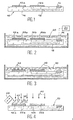
- FIGS. 1 to 4 attached illustrate the structure and use of electrode chips for the analysis of a medium.
- Figure 1 shows in section and so schematic a chip 10 of biological sensor such that used for antibody-antigen recognition or as a patient's DNA-DNA probe.
- Chip 10 includes so-called electrodes 12a and 12b and addressing electrodes 14. Although the number of electrodes on a chip analysis is generally high, on the order of one ten to several hundred, chip 10 in the figure 1 is only shown with two analysis electrodes and only one addressing electrode, for reasons obvious in clarity. The analysis electrodes can be electrically addressed by electrodes corresponding addresses. However, when the number of analysis electrodes is very important, the chip may include an addressing device multiplexed to address all analysis electrodes from a reduced number addressing electrodes.
- Addressing means linking electrical of one or more analysis electrodes with one or more so-called addressing electrodes usually around the periphery of the chip.
- the electrodes addresses allow to apply or measure a voltage on the analysis electrodes, by means of a suitable outdoor device.
- the analysis electrodes 12a and 12b are made of a metal such as, for example, gold, or platinum. They are mutually isolated from each other on a substrate plate 16. Des electrical connections between the analysis electrodes 12a, 12b and the addressing electrodes are provided in substrate 16 and are very schematically indicated with reference 18.
- a chip, as shown in Figure 1, must be configured for a particular use and the analysis electrodes are therefor made functional by garnishing them with probe molecules or by covering their surface with a reagent deposit appropriate.
- the deposition of reactive products or the grafting of probe molecules on the electrodes is made, in general, by electrodeposition.
- Reagents or probe molecules deposited on the electrodes allow, as indicated above, selective pairing with specific molecules of a substance to be analyzed. These molecules are designated by "target molecules" in the rest of the text.
- Electrolyte bath is understood to mean a bath suitable for depositing, by electrochemistry, a reagent on the electrodes, or a bath in which are diluted probe molecules to be fixed by plating on the electrodes.
- the selective application of a voltage of polarization between analysis electrodes selected and a reference electrode allows fix the reagent product or the probe molecules.
- the voltage is applied to the electrodes by means of a external generator 24 connected to the electrodes addressing 14.
- the probe molecules are fixed on the analysis electrodes, for example, using conductive polymers of polypyrrol or polyaniline type who are carriers of probe molecules.
- the chip can undergo several stages of deposition electrochemical by being soaked in different baths. So different electrodes of the chip can be covered with different reagents, or probe molecules, sensitive to different compounds of substances to analyze.
- the chip After filling the electrodes with the reagents, probe molecules, the chip is ready for be used to analyze a designated substance by analyte in the following description.
- the chip 10 is disconnected from the generator and is immersed in a bath 30 containing the analyte.
- This bath contains, for example, target molecules 32 that match or react with the reagent or the probe molecules 22a previously deposited on the first electrode 12a.
- target molecules 32 are represented schematically and magnified.
- Target molecules 32 do not interact however not with the second electrode 12b, the reactive coating, or the probe molecules, are only not compatible.
- the chip After being extracted from the analyte bath 30, the chip is analyzed to determine the electrodes for which a reaction or pairing has had location.
- the entire chip 10 is subjected to light radiation 40 of a first wavelength and coming from a source light not shown.
- the labeled target molecules absorb the light radiation 40 and emit radiation bright 42 with a second wavelength characteristic, different from the first length wave.
- a detection device 46 sensitive to the second wavelength to detect light re-emitted from the electrodes carrying the target molecules marked by the fluorescent product. It is thus possible, knowing the nature of the reagents or probe molecules previously deposited on each electrode to determine the components of the analyte who settled there.
- step pairing or hybridization during which the target molecules are attached to the probe molecules or on the reagent.
- a plurality of distinct probe molecules can thus fill the electrodes of the chip.
- Each probe molecule has a succession of bases, generally identified with the letters A, T, C and G, in a specific order.
- a strand of DNA contained in the analyte can pair with a given probe molecule when it has a base sequence complementary to a basic sequence of the probe molecule.
- Connections between the bases are of two types: hydrogen bonds A-T (bonds involving two atoms hydrogen) and hydrogen bonds C-G (bonds involving three hydrogen atoms).
- the matching reaction i.e. links between complementary bases, is reversible.
- This property is particularly important to delete accidental pairings does not not corresponding to a complete sequence of bases complementary.
- all DNA strand of the analysis comprising a sequence complete or partial complementary to the 8 bases can pair at least in part with the probe molecule.
- the temperature required for breaking the links of a paired structure depends basically from the first base of the sequence of the probe molecule.
- the object of the present invention is to provide a analysis device for performing a heating to a desired temperature for each electrode of a chip, in order to perform analyzes reliable and reproducible with chips including a large number of electrodes filled with reagents or different probe molecules.
- An object of the invention is also to propose an electronic chip analysis device allowing to precisely control the temperature in the vicinity of each electrode of the chip.
- An object of the invention is also to propose a economical chip analysis device usable in especially for genetic analysis.
- the invention has more specifically for an analysis device which has at least one chip equipped with a plurality analysis electrodes, and which further comprises means for individual heating of the electrodes analysis.
- the individual heating means of the analysis electrodes it is possible, for example, to selectively heat a selected assembly of analysis electrodes among the plurality of electrodes analysis.
- each electrode in the case of a chip comprising electrodes lined with DNA probe molecules it's possible to heat each electrode to a temperature dependent, for example, on the DNA sequence of probe molecules with which it is filled.
- the heating means may include, for each electrode, a conductive track of heating disposed in the vicinity of said electrode.
- the conductive track of heating is arranged in the vicinity of an electrode analysis when the average distance between the runway conductive of this electrode is less than the distance separating the conductive track from the others chip analysis electrodes.
- each conductive track of heater can be arranged so as to surround the electrode.
- a conductive track of heating can be respectively associated with at least a conductive track forming an electrode and extending so parallel to it.
- Individual heating means can have linked electronic addressing circuits to address electrodes, and designed to make selectively pass through each conductive track of heating a current corresponding to local heating wish.
- the current supply of the tracks conductive heating can be direct, in using a number of circuits and electrodes addressing corresponding to the number of tracks heating conductors. Power supply can also take place through circuits multiplexed.
- the heating means may include minus an electronic addressing circuit for selectively and individually apply a current of heating to the conductive tracks forming analysis electrodes. So the tracks have a double analysis and heating electrode function.
- the analysis device of the invention can also include means for mutual thermal insulation of electrodes and conductive heating tracks.
- Mutual thermal insulation means electrodes insulation to reduce heat exchanges between neighboring electrodes and between a given electrode and a conductive track of heating associated with an electrode close to said given electrode.
- the thermal insulation means can particular include a layer of polymer material, electrical insulator, placed on the chip, and on which are formed the analysis electrodes.
- This layer of polymer material is preferably chosen with a thermal conductivity lower than that of the chip.
- the means of individual heating of the analysis electrodes can also include at least a laser source and at least one network of microlenses to make a radiation of heating to selected analysis electrodes of said plurality of analysis electrodes.
- the network of microlenses can be provided with a mask presenting regions of variable density and arranged in front of microlenses.
- the microlens array can be fitted with a mask presenting regions transparent and opaque regions.
- the mask can also include regions leaving more or less pass the laser light.
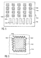
- Figure 5 shows an electronic chip according to the invention used in a device analysis.
- the chip, produced on a substrate 116 has a plurality of analysis electrodes 112 produced under the shape of metallic pellets, for example gold or platinum pellets. Each electrode can have one or more metallic pads mutually isolated.
- each electrode has a single metal chip.
- the chip also includes, in a region substrate device, addressing electrodes 114 capable of being connected to switchgear outdoor electrics through a suitable connector not shown.
- Apparatus external electrics also not shown, may include sources of current and / or voltage to allow electrochemical deposition of reactive materials or probe molecules on analysis electrodes.
- Electrical equipment may also include measuring means, for example example, to measure impedances between electrodes.
- the puce can include, for example, a set of tracks integrated conductors forming connection circuits.
- the chip can also include circuits multiplexer electronics to address a large number of analysis electrodes from a number reduced addressing electrodes.
- each analysis electrode 112 is surrounded by a turn under the shape of a conductive track 150.
- the track conductive 150 constitutes a heating resistor which, when crossed by a current, allows to raise the temperature of the electrode. She permits also to locally heat an analyte or a electrolyte which would be in contact with the electrode.
- a number addressing electrodes 114 can also be provided to selectively apply to each conductive track 150 a current suitable for the desired local heating.
- the application of the current to each conductive track can take place via a plurality of independent electrical circuits or by a multiplex type circuit.
- circuits are connected by connections internals not shown in the figure, at terminals 152 and 154 of each conductive track 150.
- the current required for heating can be applied by an appropriate current source external to the chip and connected to the electrodes addressing by a corresponding connector.
- each conductive heating track can also be used as a counter electrode. It is then used during electrochemical treatment for packing electrodes with a reagent or probe molecules.
- the conductive track is also selectively addressable to apply a electrical potential suitable for electrodeposiotion.
- Figure 6 shows, on a larger scale, a particular configuration of an analysis electrode and a conductive heating track which is associated.
- the analysis electrode 112 in the form of a square metallic patch, is surrounded by a track conductive which presents on its path, along the sides of the electrode, a square pattern. This pattern increases the length of the conductive track 150 and also to favor the heating of the electrode.
- references 152 and 154 designate the terminals of the conductive track 150.
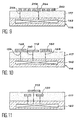
- the electrode 112 also comes in the form of a conductive track.
- the conductive track forming the electrode analysis and the conductive heating track extend substantially parallel and are folded, in this example, in the shape of a square spiral.
- the terminals of the conductive heating track are indicated with the references 152 and 154.
- Figure 8 shows yet another mode of realization of the electrode and the heating track.
- a single conductive track 250 forms at a time the analysis electrode and the heating means of this electrode.
- the conductive track 250 is folded in square spiral shape. Terminals of the track of which indicated with the references 252 and 254.
- Figure 9 is a local schematic section and partial of a substrate comprising electrodes as shown in Figure 8.
- the chip has a surface covered by a layer 117 in an electrical insulating material.
- a layer of polyimide with a thickness of the order of 15 ⁇ m.
- the conductive track 250 is formed at the surface of the insulating layer 117.
- This addressing device allows, as described above, to apply selectively a heating current at each track conductive, through electrodes addressing.
- the material used to form the layer 117 is preferably a polymer material having thermal insulation properties. So the track conductive is thermally insulated, not only from substrate 116 of the chip, but also tracks conductive forming the conductive electrodes neighbors. This thermal insulation makes it possible to make even more independent the heating of each individual electrode.
- the conductive track 250 can be covered with a thin layer 264 of a material electrical insulator.
- a substrate equipped with such electrodes can be used for analysis of electrically conductive analytes.
- the packing with a reagent is not performed electrochemically but for example with micro-pipettes.
- Figures 10 and 11 also show chip cuts according to other embodiments in which the analysis electrode is distinct from the conductive heating track.
- the track heating conductor 150 is arranged around the analysis electrode 112. It is, just like the electrode 112 itself, formed on a layer of electrical insulating material 117 which covers the substrate 116 of the chip.
- the insulating material electric can also be chosen according to its thermal insulation properties. So the track heating conductor, located in the immediate vicinity of a corresponding electrode allows the elevation in temperature of this electrode without influencing significant on neighboring electrodes.
- references 156, 158 and 160 indicate very schematically connections of electrical connection connecting the terminals respectively of the conductive heating track and the electrode analysis to addressing circuits 162, shown also schematically.
- a thin layer of electrical insulating material 164 can be formed on the conductive track of heating 150.
- This layer of insulating material electric avoids any short circuit or interaction with an analyte brought into contact with the chip.
- the insulating role of this layer is particularly advantageous when the electrolyte used is very conductive.
- Figure 11 shows a variant in which the conductive heating track 150, associated with a analysis electrode 112, is buried in the layer of electrical insulating material 117.
- the conductive track heater 150 is arranged, at least in part, under the corresponding electrode 112. It therefore occupies less of space on the surface of the chip.
- the conductive heating track is buried in the electrical insulating material 117, it is automatically electrically isolated from both the analysis electrode 112 and the analytes with which the chip is likely to be brought into contact.
- the conductive heating track is buried preferably a short distance below the surface of the layer of electrical insulation, so that sufficient thermal conduction to the electrode analysis.
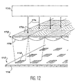
- Figure 12 shows a second implementation of the invention which does not require leads conductive heating or electrical addressing.
- the chip 110 used for this implementation of the invention simply comprises an insulating substrate 116 on which analysis electrodes are formed 112.
- the substrate can also have counter electrodes, and electrodes addressing as described above. he can also be lined with a layer of thermal insulation reducing the heat exchange between electrodes.
- the means of individual heating of analysis electrodes 112 include a laser source 170 and a network 172 of microlenses.
- the 172 microlens array receives a light beam 174 from the laser. It is placed opposite the analysis electrodes 112 of the chip 110 so as to focus the light beam 174 selectively on the electrodes 112, as indicated on Figure 12.
- the light beam concentrated on the electrodes can heat them.
- the depth of penetration of heat into the electrode is around 10 nm. Heat doesn't have time to be evacuated by the electrode.
- the laser source 170 used is, for example, a pulsed microlaser emitting in the green and presenting peak power in the range of 200 W to 800 W.
- the microlens array can include a number of microlenses corresponding to the electrodes to illuminate and therefore to heat.
- the microlens array can also have a mask with density regions 176 variable arranged to coincide with 178 microlenses on the network.
- the first term of the above expression represents the envelope.
- the function f (u) is a sine if the pupil of the microlens is square, and a Bessel function if the pupil is circular.
- the second term represents the contribution of N microlenses constituting the network. It is right to note that the intensities of the different light points obtained is not uniform. Indeed, the microlenses are large in diameter compared to no analysis electrodes and at the wavelength of the laser. To this effect is added the energy distribution of Gaussian light from the laser.
- a mask of variable density placed in front of the 178 microlenses allows if necessary to correct the non-uniformity of intensity. he is also possible not to use a mask and to put on take advantage of non-uniformity to light and therefore heat differently various chip analysis electrodes.
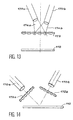
- the chip 110 is illuminated and heated by two lasers 170a, 170b.
- the beams 174a, 174b of the lasers 170a and 170b pass through a network 172 of microlenses arranged substantially parallel to the surface of the chip 110.
- the beams 174a and 174b do not are not perpendicular to the network 172 of microlenses and 110 chip.
- Lasers 170a and 170b are arranged symmetrically with respect to an axis perpendicular to the plane of the 172 microlens array and in the plane of the surface of the chip 110, and form a angle with respect to this axis.
- two separate networks 172a and 172b of microlenses are used, each network being arranged in front of a laser 170a, 170b.
- Each network is arranged substantially perpendicular to the axis of the beam of light emitted by the corresponding laser. Furthermore, lasers 170a and 170b are oriented symmetrically so that their beams form an angle with respect to an axis perpendicular to the surface of the chip 110.
- a suitable combination of one or more lasers and one or more microlens arrays allows as previously indicated to heat differently various chip analysis electrodes.
- the chip can be a more ordinary chip with no tracks heating conductors associated with the electrodes.
Description
- La figure 1, déjà décrite, est une coupe schématique d'une puce de capteur biologique.
- La figure 2, déjà décrite, est une coupe schématique de la puce de la figure 1 plongée dans un bain d'électrolyte.
- La figure 3, déjà décrite, est une coupe schématique de la puce de la figure 1, plongée dans un bain d'analyte.
- La figure 4, déjà décrite, est une coupe schématique de la puce de la figure 1, soumise à une analyse par fluorescence.
- La figure 5, est une vue schématique de dessus d'une puce électronique telle qu'utilisée dans un dispositif d'analyse conforme à l'invention.
- La figure 6 est une vue à échelle agrandie illustrant la réalisation particulière d'une électrode d'analyse de la puce électronique et d'une piste de chauffage associée.
- La figure 7 est une vue à échelle agrandie illustrant une autre réalisation possible d'une électrode d'analyse de la puce électronique et de la piste de chauffage associée.
- La figure 8 est une vue à échelle agrandie illustrant encore une autre réalisation particulière d'une électrode d'analyse de la puce électronique.
- La figure 9 est une coupe schématique locale de la puce à échelle agrandie, passant par une électrode d'analyse conforme à la figure 8.
- La figure 10 est une coupe schématique locale de la puce à échelle agrandie, passant par une électrode d'analyse et une piste conductrice de chauffage, et illustrant la structure de la puce selon une réalisation particulière.
- La figure 11 est une coupe schématique locale de la puce à échelle agrandie, passant par une électrode d'analyse et une piste conductrice de chauffage et illustrant une structure de la puce constituant une variante par rapport à la structure de la figure 10.
- La figure 12 est une vue schématique d'une variante du dispositif d'analyse conforme à l'invention.
- Les figures 13 et 14 sont des vues schématiques illustrant deux réalisations particulières du dispositif de la figure 12.
Claims (20)
- Dispositif d'analyse comportant au moins une puce (110) équipée d'une pluralité d'électrodes d'analyse (112) et caractérisé en ce qu'il comporte en outre des moyens de chauffage individuel (150, 170) des électrodes d'analyse.
- Dispositif d'analyse selon la revendication 1, dans lequel les moyens de chauffage comportent, pour chaque électrode d'analyse une piste conductrice (150, 250) de chauffage disposée au voisinage de ladite électrode.
- Dispositif d'analyse selon la revendication 2, dans lequel la piste conductrice de chauffage (150) présente un motif en serpentin.
- Dispositif d'analyse selon la revendication 2, dans lequel la piste conductrice (150) entoure ladite électrode (112).
- Dispositif selon la revendication 2, dans lequel la piste conductrice de chauffage (150) de chaque électrode d'analyse forme une contre-électrode associée à ladite électrode d'analyse.
- Dispositif d'analyse selon la revendication 2 dans lequel la piste conductrice (150) est entourée d'un matériau isolant électrique (169).
- Dispositif selon la revendication 1 comprenant des moyens d'isolation thermique (117) mutuel des électrodes d'analyse.
- Dispositif selon la revendication 7, dans lequel les moyens d'isolation thermique des électrodes comportent une couche (117) de polymère disposée sur la puce, les électrodes d'analyse (112) et les pistes conductrices de chauffage (150) étant formées sur ladite couche de polymère.
- Dispositif selon la revendication 7, dans lequel les moyens d'isolation thermique des électrodes comportent une couche (117) de polymère disposée sur la puce, les électrodes d'analyse (112) étant formées sur ladite couche de polymère et les pistes conductrices de chauffage (150) étant enterrées dans la couche de polymère, respectivement au voisinage des électrodes correspondantes.
- Dispositif selon la revendication 2 comportant des pistes conductrices (112) formant des électrodes d'analyse, une piste conductrice de chauffage étant respectivement associée à au moins une piste conductrice formant électrode d'analyse et s'étendant parallèlement à celle-ci.
- Dispositif selon la revendication 1, dans lequel la puce comporte des pistes conductrices (250) formant des électrodes d'analyse et dans lesquels les moyens de chauffage comportent au moins un circuit électronique d'adressage (162) pour appliquer sélectivement et individuellement un courant de chauffage aux pistes conductrices formant des électrodes d'analyse.
- Dispositif selon la revendication 11, les pistes conductrices formant des électrodes d'analyse (250) présentent un motif en serpentin et sont recouvertes par une couche de matériau isolant électrique (264).
- Dispositif selon la revendication 1, dans lequel les moyens de chauffage individuel de chaque électrode d'analyse comportent au moins une source laser (170, 170a, 170b) et au moins un réseau de microlentilles (172, 172a, 172b) pour faire converger un rayonnement de chauffage vers des électrodes d'analyse (112) sélectionnées de ladite pluralité d'électrode d'analyse.
- Dispositif selon la revendication 13, dans lequel le réseau de microlentille (172)est pourvu d'un masque (176) présentant des régions de densité variable, et disposées devant les microlentilles.
- Dispositif d'analyse selon la revendication 1, dans laquelle la puce est équipée d'électrodes d'adressage (114) pour appliquer sélectivement sur chaque électrode d'analyse (112) une tension dite tension d'adressage.
- Dispositif d'analyse selon la revendication 1, dans laquelle la puce est équipée d'électrodes d'adressage pour mesurer une impédance entre chaque électrode d'analyse et au moins une contre-électrode.
- Dispositif selon la revendication 15 ou 16 dans lequel les électrodes d'analyse et les électrodes d'adressage sont reliées par un circuit électronique multiplexe.
- Puce électronique comprenant une pluralité d'électrodes (112) dites électrodes d'analyse, caractérisée en ce que la puce comporte en outre, pour chaque électrode d'analyse, une piste conductrice de chauffage (150) disposée au voisinage de ladite électrode d'analyse.
- Puce électronique selon la revendication 18, comportant en outre des électrodes dites électrodes d'adressage (114) et des moyens. (162) à circuits électroniques reliant les électrodes d'adressage aux électrodes d'analyse et aux pistes conductrices de chauffage.
- Puce électronique selon la revendication 18, comprenant en outre une contre-électrode.
Applications Claiming Priority (2)
| Application Number | Priority Date | Filing Date | Title |
|---|---|---|---|
| FR9708864A FR2765967B1 (fr) | 1997-07-11 | 1997-07-11 | Dispositif d'analyse a puce comprenant des electrodes a chauffage localise |
| FR9708864 | 1997-07-11 |
Publications (2)
| Publication Number | Publication Date |
|---|---|
| EP0890651A1 EP0890651A1 (fr) | 1999-01-13 |
| EP0890651B1 true EP0890651B1 (fr) | 2002-11-13 |
Family
ID=9509153
Family Applications (1)
| Application Number | Title | Priority Date | Filing Date |
|---|---|---|---|
| EP98401743A Expired - Lifetime EP0890651B1 (fr) | 1997-07-11 | 1998-07-09 | Dispositif d'analyse à puce comprenant des électrodes a chauffage individuel |
Country Status (5)
| Country | Link |
|---|---|
| US (1) | US6255677B1 (fr) |
| EP (1) | EP0890651B1 (fr) |
| JP (1) | JPH11127900A (fr) |
| DE (1) | DE69809339T2 (fr) |
| FR (1) | FR2765967B1 (fr) |
Families Citing this family (20)
| Publication number | Priority date | Publication date | Assignee | Title |
|---|---|---|---|---|
| FR2794572B1 (fr) * | 1999-06-02 | 2003-06-13 | Commissariat Energie Atomique | Puce et procede de garniture d'une puce comprenant une pluralite d'electrodes |
| US6428749B1 (en) | 1999-12-15 | 2002-08-06 | Hitachi, Ltd. | Advanced thermal gradient DNA chip (ATGC), the substrate for ATGC, method for manufacturing for ATGC, method and apparatus for biochemical reaction, and storage medium |
| JP2001185796A (ja) | 1999-12-27 | 2001-07-06 | Hitachi Metals Ltd | レーザ装置、その応用装置並びにその使用方法 |
| US6544477B1 (en) | 2000-08-01 | 2003-04-08 | Regents Of The University Of Minnesota | Apparatus for generating a temperature gradient |
| US7527720B2 (en) | 2001-09-28 | 2009-05-05 | Mitsubishi Rayon Co., Ltd. | Device for electrophoresis, electrophoresis equipment, electrophoretic method, and specimen detection method |
| DE10208770A1 (de) * | 2002-02-28 | 2003-09-04 | Febit Ag | Erhöhung der Sensitivität und Spezifität von Hybridisierungsexperimenten mit Nukleinsäure-Chips |
| DE10324912A1 (de) * | 2003-05-30 | 2005-01-05 | Siemens Ag | Verfahren zur Detektion von DNA-Punktmutationen (SNP-Analyse) sowie zugehörige Anordnung |
| JP4464664B2 (ja) * | 2003-06-13 | 2010-05-19 | 独立行政法人理化学研究所 | 生体分子マイクロアレイ用基板、生体分子マイクロアレイ、相互作用促進用装置および方法、ならびに、相互作用の検出方法 |
| DE102004017750B4 (de) * | 2004-04-06 | 2006-03-16 | Flechsig, Gerd-Uwe, Dr. rer. nat. | Analyse-Array mit heizbaren Elektroden |
| DE102005007148B4 (de) * | 2005-02-11 | 2008-05-15 | Universität Rostock | Verfahren und Array zur Replizierung und Analytik von Nukleinsäuren |
| KR100768089B1 (ko) * | 2005-11-30 | 2007-10-18 | 한국전자통신연구원 | 친화 크로마토그래피 미세장치, 이의 제조방법. |
| DE102006006347B3 (de) * | 2006-02-07 | 2007-08-23 | Universität Rostock | Sensorvorrichtung für ein elektrochemisches Messgerät und Verfahren zur Durchführung elektrochemischer Messungen |
| EP1999272B1 (fr) * | 2006-03-21 | 2017-11-01 | Koninklijke Philips N.V. | Dispositif de detection microelectronique a reseau de capteurs |
| CN101405410B (zh) * | 2006-03-21 | 2013-06-19 | 皇家飞利浦电子股份有限公司 | 具有传感器阵列的微电子传感器装置 |
| WO2008044779A1 (fr) * | 2006-10-06 | 2008-04-17 | Sharp Kabushiki Kaisha | Structure micro-pixélisée de dosage de liquide, structure précurseur micro-pixélisée de dosage de liquide, et procédés liés à la fabrication et à la réalisation |
| US7759957B2 (en) * | 2007-07-27 | 2010-07-20 | United Microelectronics Corp. | Method for fabricating a test structure |
| DE102012219656A1 (de) * | 2012-10-26 | 2014-04-30 | Fraunhofer-Gesellschaft zur Förderung der angewandten Forschung e.V. | System zur durchführung einer berührungslosen messung an einer probe und probenträger |
| GB201314721D0 (en) * | 2013-08-16 | 2013-10-02 | Almagen Ltd | A method of selectively masking one or more sites on a surface and a method of synthesising an array of molecules |
| DE102014114047A1 (de) * | 2014-09-26 | 2016-03-31 | Universität Rostock | Verfahren und Vorrichtung zur elektrochemischen Synthese |
| US9999100B2 (en) * | 2015-04-07 | 2018-06-12 | Cell Id Pte Ltd | DC heater |
Family Cites Families (7)
| Publication number | Priority date | Publication date | Assignee | Title |
|---|---|---|---|---|
| DE2247962C3 (de) * | 1972-09-29 | 1979-03-01 | Siemens Ag, 1000 Berlin Und 8000 Muenchen | Thermoelementanordnung auf Halbleiterbasis |
| US5632957A (en) * | 1993-11-01 | 1997-05-27 | Nanogen | Molecular biological diagnostic systems including electrodes |
| CA2129787A1 (fr) * | 1993-08-27 | 1995-02-28 | Russell G. Higuchi | Surveillance de plusieurs reactions d'amplification simultanement et analyse de ces reactions simultanement |
| JP3068413B2 (ja) * | 1994-07-13 | 2000-07-24 | 日立電子エンジニアリング株式会社 | Dna塩基配列決定装置 |
| JP3566377B2 (ja) * | 1995-03-01 | 2004-09-15 | 株式会社神戸製鋼所 | ダイヤモンド薄膜バイオセンサ |
| CN1192097C (zh) * | 1995-03-10 | 2005-03-09 | 梅索磅秤技术有限公司 | 多阵列、多特异性的电化学发光检验 |
| FR2746183B1 (fr) * | 1996-03-14 | 1998-06-05 | Dispositif capteur chimique a semiconducteur et procede de formation d'un dispositif capteur chimique a semiconducteur |
-
1997
- 1997-07-11 FR FR9708864A patent/FR2765967B1/fr not_active Expired - Fee Related
-
1998
- 1998-07-08 US US09/111,773 patent/US6255677B1/en not_active Expired - Fee Related
- 1998-07-09 DE DE69809339T patent/DE69809339T2/de not_active Expired - Fee Related
- 1998-07-09 EP EP98401743A patent/EP0890651B1/fr not_active Expired - Lifetime
- 1998-07-10 JP JP10196402A patent/JPH11127900A/ja active Pending
Also Published As
| Publication number | Publication date |
|---|---|
| DE69809339D1 (de) | 2002-12-19 |
| FR2765967B1 (fr) | 1999-08-20 |
| FR2765967A1 (fr) | 1999-01-15 |
| JPH11127900A (ja) | 1999-05-18 |
| DE69809339T2 (de) | 2003-09-18 |
| EP0890651A1 (fr) | 1999-01-13 |
| US6255677B1 (en) | 2001-07-03 |
Similar Documents
| Publication | Publication Date | Title |
|---|---|---|
| EP0890651B1 (fr) | Dispositif d'analyse à puce comprenant des électrodes a chauffage individuel | |
| EP0882981A1 (fr) | Microsystème d'analyse de liquides à cuvette intégrée | |
| US7480433B2 (en) | Electro-optical stimulation/measurement | |
| WO1998057157A1 (fr) | Procede d'identification et/ou de dosage de substances biologiques, presentes dans un liquide conducteur, dispositif et capteur d'affinite utiles pour la mise en oeuvre de ce procede | |
| FR2795426A1 (fr) | Support d'analyse biologique a amplification | |
| FR2781886A1 (fr) | Micro-systeme a multiple points d'analyse chimique ou biologique | |
| EP0882979B1 (fr) | Support d'électrodes comportant au moins une électrode recouverte par un dépot et système de lecture de ce support | |
| US8623283B2 (en) | Combined electrical and optical sensor for fluids | |
| EP0883699B1 (fr) | Procede et dispositifs pour la formation electrolytique d'un depot sur un ensemble selectionne d'electrodes | |
| FR2843757A1 (fr) | Procede de garniture d'une surface par un film organique | |
| EP2343543A1 (fr) | Capteur biologique à mesure électrochimique et/ou électrique et à électrode de diamant et circuit électronique intégrés | |
| EP3853606B1 (fr) | Dispositif microfluidique et procédés d'utilisation dudit dispositif | |
| EP1186048A1 (fr) | Puce et procede de garniture d'une puce comprenant une pluralite d'electrodes | |
| FR2952800A1 (fr) | Dispositif electrochimique pour la determination de proprietes antioxydantes de la peau | |
| EP0780890B1 (fr) | Procédé de dépot électrochimique | |
| EP0882980A1 (fr) | Traitement de surface d'un substrat limitant sa fluorescence naturelle | |
| WO2014041145A1 (fr) | Procede et dispositif de mesure quantitative par libs de cibles biomoleculaires sur bio-puce | |
| JP2021081239A (ja) | プローブ型センサー | |
| FR2746678A1 (fr) | Procede de realisation d'un depot sur un support amovible, et depot realise sur un support | |
| EP2939007B1 (fr) | Procede et dispositif pour caracteriser un milieu fluide a l'aide d'un substrat semi-conducteur | |
| EP1869439A1 (fr) | Procede d'analyse electrochimique par voltametrie et dispositif pour sa mise en oeuvre | |
| FR2772926A1 (fr) | Dispositif et procede de test d'elements sensibles d'une puce electronique | |
| FR2842604A1 (fr) | Systeme de detection d'au moins une substance chimique | |
| WO2018115489A1 (fr) | Dispositif de cellules électrochimiques et système de mesure électrochimique comprenant un tel dispositif | |
| FR2635414A1 (en) | Optical switching device and applications to circuit testing |
Legal Events
| Date | Code | Title | Description |
|---|---|---|---|
| PUAI | Public reference made under article 153(3) epc to a published international application that has entered the european phase |
Free format text: ORIGINAL CODE: 0009012 |
|
| AK | Designated contracting states |
Kind code of ref document: A1 Designated state(s): BE DE GB IT |
|
| AX | Request for extension of the european patent |
Free format text: AL;LT;LV;MK;RO;SI |
|
| 17P | Request for examination filed |
Effective date: 19990615 |
|
| AKX | Designation fees paid |
Free format text: BE DE GB IT |
|
| GRAG | Despatch of communication of intention to grant |
Free format text: ORIGINAL CODE: EPIDOS AGRA |
|
| RTI1 | Title (correction) |
Free format text: ANALYSING CHIP WITH INDIVIDUALLY HEATABLE ELECTRODES |
|
| 17Q | First examination report despatched |
Effective date: 20010724 |
|
| GRAG | Despatch of communication of intention to grant |
Free format text: ORIGINAL CODE: EPIDOS AGRA |
|
| GRAH | Despatch of communication of intention to grant a patent |
Free format text: ORIGINAL CODE: EPIDOS IGRA |
|
| GRAH | Despatch of communication of intention to grant a patent |
Free format text: ORIGINAL CODE: EPIDOS IGRA |
|
| GRAH | Despatch of communication of intention to grant a patent |
Free format text: ORIGINAL CODE: EPIDOS IGRA |
|
| GRAA | (expected) grant |
Free format text: ORIGINAL CODE: 0009210 |
|
| AK | Designated contracting states |
Kind code of ref document: B1 Designated state(s): BE DE GB IT |
|
| REG | Reference to a national code |
Ref country code: GB Ref legal event code: FG4D Free format text: NOT ENGLISH |
|
| REF | Corresponds to: |
Ref document number: 69809339 Country of ref document: DE Date of ref document: 20021219 |
|
| GBT | Gb: translation of ep patent filed (gb section 77(6)(a)/1977) |
Effective date: 20030217 |
|
| PLBE | No opposition filed within time limit |
Free format text: ORIGINAL CODE: 0009261 |
|
| STAA | Information on the status of an ep patent application or granted ep patent |
Free format text: STATUS: NO OPPOSITION FILED WITHIN TIME LIMIT |
|
| 26N | No opposition filed |
Effective date: 20030814 |
|
| PGFP | Annual fee paid to national office [announced via postgrant information from national office to epo] |
Ref country code: GB Payment date: 20050706 Year of fee payment: 8 |
|
| PGFP | Annual fee paid to national office [announced via postgrant information from national office to epo] |
Ref country code: DE Payment date: 20050730 Year of fee payment: 8 |
|
| PGFP | Annual fee paid to national office [announced via postgrant information from national office to epo] |
Ref country code: BE Payment date: 20050914 Year of fee payment: 8 |
|
| PG25 | Lapsed in a contracting state [announced via postgrant information from national office to epo] |
Ref country code: GB Free format text: LAPSE BECAUSE OF NON-PAYMENT OF DUE FEES Effective date: 20060709 |
|
| PG25 | Lapsed in a contracting state [announced via postgrant information from national office to epo] |
Ref country code: BE Free format text: LAPSE BECAUSE OF NON-PAYMENT OF DUE FEES Effective date: 20060731 |
|
| PGFP | Annual fee paid to national office [announced via postgrant information from national office to epo] |
Ref country code: IT Payment date: 20060731 Year of fee payment: 9 |
|
| PG25 | Lapsed in a contracting state [announced via postgrant information from national office to epo] |
Ref country code: DE Free format text: LAPSE BECAUSE OF NON-PAYMENT OF DUE FEES Effective date: 20070201 |
|
| GBPC | Gb: european patent ceased through non-payment of renewal fee |
Effective date: 20060709 |
|
| BERE | Be: lapsed |
Owner name: COMMISSARIAT A L'ENERGIE *ATOMIQUE Effective date: 20060731 |
|
| PG25 | Lapsed in a contracting state [announced via postgrant information from national office to epo] |
Ref country code: IT Free format text: LAPSE BECAUSE OF NON-PAYMENT OF DUE FEES Effective date: 20070709 |