EP0882962A2 - Dispositif pour mesurer de la lumière, permettant de mesurer le niveau de la puissance optique facilement et avec précision - Google Patents
Dispositif pour mesurer de la lumière, permettant de mesurer le niveau de la puissance optique facilement et avec précision Download PDFInfo
- Publication number
- EP0882962A2 EP0882962A2 EP98110236A EP98110236A EP0882962A2 EP 0882962 A2 EP0882962 A2 EP 0882962A2 EP 98110236 A EP98110236 A EP 98110236A EP 98110236 A EP98110236 A EP 98110236A EP 0882962 A2 EP0882962 A2 EP 0882962A2
- Authority
- EP
- European Patent Office
- Prior art keywords
- section
- photo
- light
- detecting section
- current
- Prior art date
- Legal status (The legal status is an assumption and is not a legal conclusion. Google has not performed a legal analysis and makes no representation as to the accuracy of the status listed.)
- Granted
Links
- 230000003287 optical effect Effects 0.000 title abstract description 43
- 238000005259 measurement Methods 0.000 claims abstract description 26
- 229910000530 Gallium indium arsenide Inorganic materials 0.000 claims description 10
- 239000000835 fiber Substances 0.000 description 32
- 238000006243 chemical reaction Methods 0.000 description 12
- 238000000034 method Methods 0.000 description 8
- 238000010586 diagram Methods 0.000 description 7
- 238000005070 sampling Methods 0.000 description 4
- 230000005540 biological transmission Effects 0.000 description 3
- 230000007423 decrease Effects 0.000 description 3
- 230000001960 triggered effect Effects 0.000 description 3
- 230000005611 electricity Effects 0.000 description 2
- 230000003247 decreasing effect Effects 0.000 description 1
- 230000002950 deficient Effects 0.000 description 1
- 230000000694 effects Effects 0.000 description 1
- 238000000253 optical time-domain reflectometry Methods 0.000 description 1
Images


Classifications
-
- G—PHYSICS
- G01—MEASURING; TESTING
- G01J—MEASUREMENT OF INTENSITY, VELOCITY, SPECTRAL CONTENT, POLARISATION, PHASE OR PULSE CHARACTERISTICS OF INFRARED, VISIBLE OR ULTRAVIOLET LIGHT; COLORIMETRY; RADIATION PYROMETRY
- G01J1/00—Photometry, e.g. photographic exposure meter
- G01J1/42—Photometry, e.g. photographic exposure meter using electric radiation detectors
- G01J1/44—Electric circuits
Definitions
- This invention relates to a light measuring device, and more particularly to a light measuring device capable of measuring the power level of incident light.
- a light measuring device such as an optical power meter
- the offset level of the photo-detecting system e.g., an amplifier
- the offset level is defined as the output level of the photo-detecting system on which no light from the object to be measured is projected.
- the accurate optical power of light from the measured object can be calculated by subtracting the offset level from the output level of the photo-detecting system on which the light from the measured object has been projected.
- the subtraction process is called offset compensation.
- a shade cover is put on the connector section of the light measuring device to which an object to be measured is connected.
- the output level of the light measuring device whose connector section has not been struck by light is measured and the measured level is determined to be the offset level.
- the shade cover is removed and an object to be measured is connected to the connector section of the light measuring device. Then, the light from the object is allowed to strike the connector section.
- the previously determined offset level is subtracted from the level of the light sensed by the photo-detecting system of the light measuring device at that time. In this way, the resulting level is measured as the optical power level of light from the measured object.
- the offset compensation is made periodically to reduce measurement errors.
- the conventional light measuring devices prevent the desired measuring operation from being started immediately.
- FIG. 2 shows a characteristic of the output current, dark current, and current multiplication factor of an InGaAs APD (Avalanche Photodiode) versus reverse voltage.
- the dark current is added to the received-light current caused by the light from the measured object.
- the APD outputs the resulting current.
- FIG. 3 shows the calculated measurement error by the dark current in this condition corresponding to the optical power.
- One known light measuring device is an OTDR (an Optical Time Domain Reflectometer), which throws light pulse on a fiber to be measured, processes the reflected light (back scattering light or Fresnel reflected light) from the measured fiber as a result of the supply of the light pulse, and measures losses or defective points in the measured fiber.
- OTDR an Optical Time Domain Reflectometer
- FIG. 6 shows a general configuration of an OTDR of this type.
- the OTDR comprises a timing generator section 21, a light pulse emitting section 22, a branch section 23, a photo-detecting section 24, a direct-current amplifying section 25, an A/D conversion section 26, a processing section 27, and a display section 28.
- the timing generator section 21 outputs a signal to the light pulse emitting section 22 in a period corresponding to the length of a fiber 29 to be measured, that is, in the period T longer than time t required for the reflected light to come back the total length of the fiber 29 since the supply of the light pulse to the fiber 29.
- the light pulse generator section 22 receives the output, the light pulse generator section 22 generates a light pulse in each period T .
- the light pulse generated in each period T by the light pulse generator section 22 is allowed to input the fiber 29 via the branch section 23.
- the reflected light returning from the fiber 29 as a result of the supply of the light pulse is allowed to input the photo-detecting section 24 via the branch section 23, which converts the light into electricity.
- the photoelectrically converted signal is converted by the A/D converter section 26 into a digital signal.
- the digital signal is inputted to the processing section 27.
- the processing section 27 performs the process of logarithmically converting the inputted digital signal by sampling the data.
- a light pulse is thrown to the fiber 29 in each period T (e.g., at intervals of one msec).
- the average value of an M number of (e.g., 20) data items not containing the reflected light from the fiber 29 is determined to be the offset level.
- offset compensation is made by subtracting the offset level from each of the N number of data items sampled.
- Recent OTDRs are required to have the function of measuring the power level of the incident light from the object, such as a light source or a light transmission device.
- the received-light power level of incident light is measured without using a light pulse from the light pulse emitting section 22.
- offset compensation for the photo-detecting system must be made in the OTDR as in generally used light measuring devices.
- an object of the present invention to solve the problem of the above-described prior art by providing a light measuring device capable of easily measuring, with high accuracy, the received-light power level of light from an object to be measured by effecting offset compensation without shading light before measurement as in the prior art.
- a light measuring device comprising: a photo-detecting section whose output current varies according to an applied reverse bias voltage and which receives light from a measured object and outputs a current proportional to the intensity of the light; a bias section which generates a first reverse voltage to prevent the output current of the photo-detecting section from flowing and a second reverse bias voltage to allow the output current of the photo-detecting section to flow and applies the first reverse bias voltage and the second reverse bias voltage to the photo-detecting section; a direct-current amplifying section which outputs a signal whose level is proportional to the output current from the photo-detecting section; and a processing section which determines the intensity of light from the measured object from a first output from the direct-current amplifying section when the bias section is controlled so that the first reverse bias voltage may be applied to the photo-detecting section and a second output from the direct-current amplifying section when the bias section is controlled so that the second reverse bias voltage may be applied to the photo-detecting section.
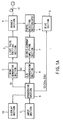
- FIG. 1A An outline of a light measuring device according to the present invention will be explained by reference to FIG. 1A.
- light measuring devices In the knowledge that if optical power is in the range down to about -50 dBm, the power level of the incident light from an object to be measured can be measured with sufficient accuracy by compensating for only the offset level due to the factor 2 which is aforementioned, light measuring devices according to the present invention have the following configurations.
- a light measuring device is characterized by comprising: a photo-detecting section 5 whose output current varies with an applied reverse bias voltage and which receives light from an object to be measured; a bias section 6 which applies a reverse bias voltage to the photo-detecting section in such a manner that the bias voltage can vary; a direct-current amplifying section which outputs a signal whose level is proportional to the output current from the photo-detecting section; and means 8 and 9 which determine a first output level outputted from the direct-current amplifying section when the bias section applies the reverse bias voltage to the photo-detecting section to prevent the output current from flowing, determine a second output level outputted from the direct-current amplifying section when the bias section applies the reverse bias voltage to the photo-detecting section to allow the output current to flow, and determine the optical power level of the object by subtracting the first output level from the second output level to compensate for an offset.
- a light measuring device is characterized in that in the light measuring device according to the first aspect of the present invention, the bias section 6 applies to the photo-detecting section such a reverse bias voltage as makes the current multiplication factor of the photo-detecting section almost zero to prevent the output current of the photo-detecting section 5 from flowing and applies to the photo-detecting section such a reverse bias voltage as makes the current multiplication factor of the photo-detecting section one or more to allow the output current of the photo-detecting section 5 to flow to enable the measurement of the optical power level of the measured object.
- the bias section 6 applies to the photo-detecting section such a reverse bias voltage as makes the current multiplication factor of the photo-detecting section almost zero to prevent the output current of the photo-detecting section 5 from flowing and applies to the photo-detecting section such a reverse bias voltage as makes the current multiplication factor of the photo-detecting section one or more to allow the output current of the photo-detecting section 5 to flow to enable the measurement of the optical power level of the measured object.
- means 8 and 9 determine the first output level outputted from the direct-current amplifying section 7 when the bias section 6 applies a reverse bias voltage to the photo-detecting section 5 to prevent the output current of the photo-detecting section 5 from flowing.
- the means 8 and 9 determine the second output level outputted from the direct-current amplifying section 7 when the bias section 6 applies a reverse bias voltage to the photo-detecting section 5 to allow the output current of the photo-detecting section 5 to flow.
- the means 8 and 9 determine the optical power level of the object by subtracting the first output level from the second output level to compensate for the offset.
- the present invention it is possible to provide a light measuring device capable of easily measuring the power level of the incident light from the measured object with high accuracy by performing offset compensation without shading light before measurement as in the prior art.
- FIG. 1A is a block diagram of a light measuring device according to a first embodiment of the present invention.
- the light measuring device comprises an input section 1, a timing generator section 2, a light pulse emitting section 3, a branch section 4, a photo-detecting section 5, a bias section 6, a direct-current amplifying section 7, an A/D conversion section 8, a processing section 9, and a display section 10.
- the input section 1 has a fiber measuring mode and an optical power level measuring mode and chooses one of these modes as a result of key operation.
- the input section 1 outputs the signal corresponding to the chosen mode to the processing section 9 as described later.
- the input section 1 also outputs the various measuring parameters necessary for signal processing to the processing section 9.
- the timing generator section 2 On the basis of a control signal S1 from the processing section 9, the timing generator section 2 outputs a timing signal S2 to the light pulse emitting section 3 and A/D conversion section 8.
- the light pulse emitting section 3 Being triggered by the timing signal S2 from the timing generator section 2, the light pulse emitting section 3 outputs a light pulse in a long wavelength band of, for example, 1.3 ⁇ m or 1.55 ⁇ m.
- the light pulse from the light pulse emitting section 3 is emitted via the branch section 4 to the measured fiber 11 in the period corresponding to the length of the fiber 11, that is, in the period T longer than time t required for the reflected light to come back the total length of the fiber 11 since the supply of the light pulse to the fiber 11.
- the branch section 4 is composed of, for example, a directional optical coupler and branches to the side of the photo-detecting section 5 the reflected light (back scattering light or Fresnel reflected light) from the fiber 11 as a result from the supply of light pulse in the fiber measuring mode or the incident light from the object to be measured, such as a light source or an optical transmission, in the power level measuring mode.
- the photo-detecting section 5 is composed of, for example, InGaAs APD, and has the function of amplifying electrons or holes created by the incident light at a specific current multiplication factor.
- the photo-detecting section 5 senses not only the reflected light from the fiber 11 separated by the branch section 4 in the fiber measuring mode but also the incident light from the measured object in the optical power level measuring mode.
- the current multiplication factor M of the photo-detecting section 5 is changed according to the level of the reverse bias voltage applied by the bias section 6.
- An InGaAs APD having a characteristic of the output current, dark current, and current multiplication factor versus the reverse voltage shown in FIG. 2 is used as the photo-detecting section 5.
- the offset due to the dark current in the photo-detecting section 5 has a negligible value as analyzed in BACKGROUND OF THE INVENTION.
- the photo-detecting section 5 is not restricted to the InGaAs APD and may be any suitable device, provided that the variation of the reverse bias voltage allows almost no output current of the device to flow.
- the bias section 6 On the basis of a control signal S3 from the processing section 9, the bias section 6 applies a specific reverse bias voltage to the photo-detecting section 5.
- the bias section 6 receiving a control signal S3a for an offset compensation instruction from the processing section 9, applies to the photo-detecting section 5 such a reverse bias voltage (e.g., in the rage of 0V or higher and 13V or lower) as makes the current multiplication factor M almost 0 at which almost no current flows in the photo-detecting section 5.
- a reverse bias voltage e.g., in the rage of 0V or higher and 13V or lower
- the bias section 6 when receiving a control signal S3b for a measurement instruction from the processing section 9, applies to the photo-detecting section 5 such a reverse bias voltage (e.g., in the range of 16V or higher and 100V or lower) as makes the current multiplication factor M meet M ⁇ 1 to measure the incident light from the measured object.
- a reverse bias voltage e.g., in the range of 16V or higher and 100V or lower
- the direct-current amplifying section 7 amplifies the output current from the photo-detecting section 5 at a specific multiplication factor and outputs the result to the A/D conversion section 8.
- the direct-current amplifying section 7 is composed of, for example, a current-voltage converter and a voltage amplifier.
- the current-voltage converter converts the current signal outputted from the cathode of the photo-detecting section 5 into a voltage signal.
- the voltage amplifier then amplifies the converted voltage signal at a specific multiplication factor.
- the multiplication factor of the voltage amplifier in the direct-current amplifying section 7 is varied by the control signal from the processing section 9.
- the A/D conversion section 8 samples the signal amplified at the direct-current amplifying section 7 in a specific sampling period and digitizes the sampled signal. Then, the A/D conversion section outputs the sampled digital signal to the processing section 9.
- the A/D conversion section 8 converts the signal amplified at the direct-current amplifying section 7 into a digital signal and outputs it to the processing section 9.
- the processing section 9 performs the process of logarithmically converting the sampling signal from the A/D conversion section 8 in the fiber measuring mode.
- Each data item obtained from the signal processing is displayed as, for example, waveform data, on the display section 10, such as a CRT display.
- the processing section 9 performs the process of calculating an optical power level from the digital signal from the A/D conversion section 8 in the optical power level measuring mode.
- the data on the optical power level obtained by the calculation process is displayed on the display section 10.
- the processing section 9 outputs control signals S1 and S3 (S3a and S3b) to the timing generator section 2 and the bias section 6.
- the processing section 9 is composed of, for example, a CPU, and has a timer circuit in it.
- the processing section 9 outputs the control signal S3a indicating an offset instruction to the bias section 6 each time the time set in the timer circuit has elapsed.
- the processing section 9 When not outputting the control signal S3a indicating an offset compensation instruction, the processing section 9 outputs the control signal indicating a measurement instruction to the bias section 6.
- the processing section 9 outputs the control signal S1 instructing the timing generator section 2 to emit a light pulse.
- the light pulse emitting section 3 is prevented from emitting a light pulse and the incident light from the object to be measured is thrown to the photo-detecting section 5. Then, the photo-detecting section 5 performs photoelectric conversion.
- control signal S3a indicating an offset compensation instruction to the bias section 6.
- the bias section 6 When receiving control signal S3a from the processing section 9, the bias section 6 applies to the photo-detecting section 5 such a bias voltage (0) as makes the current multiplication factor M of the photo-detecting section 5 almost 0.
- the output, including dark current, of the photo-detecting section 5 is amplified at the direct-current amplifying section 7 and then, together with the offset voltage from the direct-current amplifying section 7, is converted into a digital signal at the A/D conversion section 8.
- the digital signal is then inputted to the processing section 9 as offset data in the optical power level measuring mode.
- the offset data is stored in, for example, a memory (not shown) within the processing section 9.
- the time from when such a bias voltage (0) as makes the current multiplication factor M of the photo-detecting section 5 almost 0 is applied until such a bias voltage (-V) as makes the current multiplication factor M of the photo-detecting section 5 meet M ⁇ 1 is applied is determined to be an offset data acquisition period.
- the bias section 6 When receiving control signal S3b indicting a measurement instruction from the processing section 9, the bias section 6 applies to the photo-detecting section 5 such a bias voltage (-V) as makes the current multiplication factor M of the photo-detecting section 5 meet M ⁇ 1 to bring the photo-detecting section 5 into the measurement state.
- a bias voltage (-V) as makes the current multiplication factor M of the photo-detecting section 5 meet M ⁇ 1 to bring the photo-detecting section 5 into the measurement state.
- the output current from the photo-detecting section 5 is converted into a voltage and the voltage result is amplified at the direct-current amplifying section 7.
- the signal amplified at the direct-current amplifying section 7, together with the offset voltage from the direct-current amplifying section 7, is converted into a digital signal at the A/D conversion section 8.
- the digital signal is then inputted to the processing section 9.
- the processing section 9 performs offset compensation by subtracting the offset data measured and stored at the time of the preceding offset compensation instruction (that is, when the current multiplication factor M of the photo-detecting section 5 meets M ⁇ 0) from the data of the digital signal inputted at that time.
- the level of the data after the offset compensation is the correct optical power level of the measured object.
- the time from when such a bias voltage (-V) as makes the current multiplication factor M of the photo-detecting section 5 meet M ⁇ 1 is applied until such a bias voltage (0) as makes the current multiplication factor M of the photo-detecting section 5 almost 0 is applied is determined to be allocated to the measurement state.
- the offset data when the current multiplication factor M of the photo-detecting section 5 becomes almost 0 is acquired repeatedly at intervals of time T0.
- the optical power of the incident light when the current multiplication factor M of the photo-detecting section 5 meets M ⁇ 1 is measured more than once with a faster clock than T0.
- the already acquired offset data is subtracted from each measurement data item and the level after the subtraction is displayed.
- the relationship between the measurement and display of the optical power of the incident light and the acquisition of the offset data depends on the temperature in an environment where the device is used.
- time T0 should be set shorter to acquire the offset data at shorter intervals.
- Offset compensation in the first embodiment can be made even when no light is incident on the photo-detecting section 5.
- control signal S1 indicating the emission of a light pulse
- the light pulse emitting section 3 Being triggered by timing signal S2 from the timing generator section 2, the light pulse emitting section 3 emits a light pulse via the branch section 4 to the fiber 11 to be measured.
- the light pulse emitting section 3 emits the light pulse repeatedly in the period corresponding to the length of the fiber 11, that is, in the period T longer than time t required for the reflected light to come back the total length of the fiber 11 since the supply of the light pulse to the fiber 11.
- the reflected light returning from the fiber 11 as a result of the supply of the light pulse is allowed to incident on the photo-detecting section 5 via the branch section 4. Then, the photo-detecting section 5 converts the light into electricity.
- the photoelectrically converted signal is amplified by the direct-current amplifying section 7 and is converted by the A/D converter section 8 into a digital signal.
- the digital signal is then inputted to the processing section 9.
- the processing section 9 performs the process of logarithmically converting the inputted digital signal by sampling the data.
- the waveform is displayed on the display section 10.
- a light pulse is thrown to the fiber 11 in each period T (e.g., at intervals of one msec).
- the average value of an M number of (e.g., 20) data items not containing the reflected light from the fiber 11 is determined to be the offset level. Then, offset compensation is made by subtracting the offset level from the N number of data items sampled.
- FIG. 1B is a detailed diagram of the bias section 6 in the light measuring device according to the first embodiment.
- a step-up section 61 raises an input direct-current voltage (+5 VDC) from the input terminal (IN) to an alternating-current voltage (140 VAC) and supplies the alternating-current voltage to a rectifier section 62.
- the rectifier section 62 full-wave rectifies the alternating-current voltage (140 VAC) and supplies the rectified voltage to the collector of a transistor 63.
- the emitter of the transistor 63 is connected to a voltage output terminal (OUT) serving as the bias section 6.
- An output voltage sensing section 64 divides the output voltage at the voltage output terminal (OUT) and outputs the divided voltage to an error amplifier 65.
- the error amplifier 65 compares the output from the output voltage sensing section 64 with a reference voltage (2.5 VDC) from a reference voltage generator section 66 and controls the base of the transistor 63 so that the difference between the output and the reference voltage may be kept constant.
- the reference voltage from the reference voltage generator section 66 is set variably by a digital control variable resistor 67.
- the digital control variable resistor 67 is controlled by, for example, a 4-bit control signal from the processing section 9.
- a specific reverse bias voltage can be applied to the photo-detecting section 5 by causing the digital control variable resistor 67 to set the reference voltage from the reference voltage generator section 66 variably.
- FIG. 5 is a block diagram of a light measuring device according to a second embodiment of the present invention.
- the light measuring device of the second embodiment is constructed by eliminating the timing generator section 2, light pulse emitting section 3, and branch section 4 from the light measuring device of the first embodiment.
- the light measuring device of the second embodiment is the same as that of the first embodiment except that the fiber measuring mode is absent.
- the optical power level measuring mode in the first embodiment can be set when the power supply is turned on.
- the signal at the time when the optical power level measuring mode is chosen has been used as a trigger signal.
- the signal at the time when the power switch is turned on has been used as a trigger signal. With these trigger signals, the offset data has been acquired at intervals of time T0 while the optical power level measuring mode or the power switch is on.
- the input section 1 may be provided with a separate key to select the offset mode. Then, the processing section 9 may be allowed to output an offset compensation instruction or a measurement instruction to the bias section 6, depending on whether the signal at the time when the offset mode is chosen is present or absent, which provides variable control of the reverse bias voltage applied to the photo-detecting section 5.
Applications Claiming Priority (3)
| Application Number | Priority Date | Filing Date | Title |
|---|---|---|---|
| JP14946397A JP3276306B2 (ja) | 1997-06-06 | 1997-06-06 | 光測定器 |
| JP14946397 | 1997-06-06 | ||
| JP149463/97 | 1997-06-06 |
Publications (3)
| Publication Number | Publication Date |
|---|---|
| EP0882962A2 true EP0882962A2 (fr) | 1998-12-09 |
| EP0882962A3 EP0882962A3 (fr) | 2000-03-15 |
| EP0882962B1 EP0882962B1 (fr) | 2004-12-22 |
Family
ID=15475688
Family Applications (1)
| Application Number | Title | Priority Date | Filing Date |
|---|---|---|---|
| EP98110236A Expired - Lifetime EP0882962B1 (fr) | 1997-06-06 | 1998-06-04 | Dispositif pour mesurer de la lumière, permettant de mesurer le niveau de la puissance optique facilement et avec précision |
Country Status (4)
| Country | Link |
|---|---|
| US (1) | US6043480A (fr) |
| EP (1) | EP0882962B1 (fr) |
| JP (1) | JP3276306B2 (fr) |
| DE (1) | DE69828219T2 (fr) |
Cited By (1)
| Publication number | Priority date | Publication date | Assignee | Title |
|---|---|---|---|---|
| CN102759400A (zh) * | 2011-04-25 | 2012-10-31 | 三星电子株式会社 | 光感测装置和驱动光感测装置的方法 |
Families Citing this family (7)
| Publication number | Priority date | Publication date | Assignee | Title |
|---|---|---|---|---|
| JP4660113B2 (ja) * | 2004-04-27 | 2011-03-30 | 株式会社東芝 | ファイバブラッググレーティング物理量計測装置 |
| US7619727B2 (en) * | 2006-06-07 | 2009-11-17 | Raybit Systems Inc. | Apparatus for detecting wavelength and measuring optical power |
| JP5266785B2 (ja) | 2008-02-19 | 2013-08-21 | 富士通株式会社 | 光検出装置および光検出方法 |
| JP4644732B2 (ja) * | 2008-09-18 | 2011-03-02 | シャープ株式会社 | 光変調型検出装置および電子機器 |
| US9354113B1 (en) * | 2010-11-05 | 2016-05-31 | Stc.Unm | Impact ionization devices under dynamic electric fields |
| US10128398B1 (en) | 2014-05-23 | 2018-11-13 | Stc.Unm | Resonance avalanche photodiodes for dynamic biasing |
| WO2022221141A1 (fr) * | 2021-04-12 | 2022-10-20 | Milwaukee Electric Tool Corporation | Système de niveau laser à alignement de détecteur automatique |
Citations (3)
| Publication number | Priority date | Publication date | Assignee | Title |
|---|---|---|---|---|
| US4310243A (en) * | 1979-10-19 | 1982-01-12 | Beckman Instruments, Inc. | Spectrophotometer with photomultiplier tube dark signal compensation |
| US4924081A (en) * | 1987-09-22 | 1990-05-08 | Minolta Camera Kabushiki Kaisha | Photo-electric converter having offset voltage correcting function |
| US5043608A (en) * | 1989-08-24 | 1991-08-27 | Tektronix, Inc. | Avalanche photodiode non-linearity cancellation |
Family Cites Families (3)
| Publication number | Priority date | Publication date | Assignee | Title |
|---|---|---|---|---|
| US3581643A (en) * | 1967-05-02 | 1971-06-01 | Yashica Co Ltd | Light measuring device |
| US3687558A (en) * | 1971-07-16 | 1972-08-29 | Us Air Force | Laser power-energy meter |
| WO1988007700A1 (fr) * | 1987-03-30 | 1988-10-06 | Anritsu Corporation | Generateur de signaux lumineux et systeme d'etalonnage d'un appareil de mesure de la puissance lumineuse utilisant ledit generateur |
-
1997
- 1997-06-06 JP JP14946397A patent/JP3276306B2/ja not_active Expired - Fee Related
-
1998
- 1998-06-02 US US09/088,914 patent/US6043480A/en not_active Expired - Lifetime
- 1998-06-04 EP EP98110236A patent/EP0882962B1/fr not_active Expired - Lifetime
- 1998-06-04 DE DE69828219T patent/DE69828219T2/de not_active Expired - Lifetime
Patent Citations (3)
| Publication number | Priority date | Publication date | Assignee | Title |
|---|---|---|---|---|
| US4310243A (en) * | 1979-10-19 | 1982-01-12 | Beckman Instruments, Inc. | Spectrophotometer with photomultiplier tube dark signal compensation |
| US4924081A (en) * | 1987-09-22 | 1990-05-08 | Minolta Camera Kabushiki Kaisha | Photo-electric converter having offset voltage correcting function |
| US5043608A (en) * | 1989-08-24 | 1991-08-27 | Tektronix, Inc. | Avalanche photodiode non-linearity cancellation |
Cited By (2)
| Publication number | Priority date | Publication date | Assignee | Title |
|---|---|---|---|---|
| CN102759400A (zh) * | 2011-04-25 | 2012-10-31 | 三星电子株式会社 | 光感测装置和驱动光感测装置的方法 |
| CN102759400B (zh) * | 2011-04-25 | 2017-06-06 | 三星电子株式会社 | 光感测装置和驱动光感测装置的方法 |
Also Published As
| Publication number | Publication date |
|---|---|
| EP0882962A3 (fr) | 2000-03-15 |
| JPH10339667A (ja) | 1998-12-22 |
| DE69828219T2 (de) | 2005-12-15 |
| EP0882962B1 (fr) | 2004-12-22 |
| JP3276306B2 (ja) | 2002-04-22 |
| DE69828219D1 (de) | 2005-01-27 |
| US6043480A (en) | 2000-03-28 |
Similar Documents
| Publication | Publication Date | Title |
|---|---|---|
| US4553848A (en) | Method of detecting and evaluating photometric signals and device for carrying out the method | |
| CN106463565A (zh) | 激光雷达扫描仪校准 | |
| US7324218B2 (en) | Method and device for distance measurement | |
| EP0882962B1 (fr) | Dispositif pour mesurer de la lumière, permettant de mesurer le niveau de la puissance optique facilement et avec précision | |
| US4904088A (en) | Method and apparatus for determining radiation wavelengths and wavelength-corrected radiation power of monochromatic light sources | |
| US4128339A (en) | Automatically-adjusting photometer | |
| JPH04225132A (ja) | 光学欠点発見装置 | |
| US4797556A (en) | Optical continuity testing apparatus with pulsating transmitter | |
| JPS6061634A (ja) | 温度測定装置 | |
| EP3465125B1 (fr) | Otdr à précision accrue et zone morte réduite utilisant la superposition d'impulsions avec variation de retard de signal d'horloge | |
| JPH01202614A (ja) | アクティブ測距装置 | |
| US5185635A (en) | Method of calibrating and controlling the optical power output of an OTDR | |
| KR100335597B1 (ko) | 광학식거리측정장치및방법 | |
| US6661453B1 (en) | Image input apparatus and method | |
| US20060192573A1 (en) | Method and device for determining a characteristic of a semicondctor sample | |
| JP2012132815A (ja) | Apdの自動調整機能を備えた光パルス試験器またはその方法 | |
| JP4629823B2 (ja) | 光波測距儀 | |
| JPH1151808A (ja) | 測定装置 | |
| JP3334556B2 (ja) | 分光放射照度計 | |
| WO2007016976A1 (fr) | Analyse par reflectometrie optique a partir de signaux de diffusion du premier ordre et du second ordre | |
| JP2525980B2 (ja) | 光ファイバ式温度分布測定装置 | |
| JPH02309220A (ja) | 光ファイバ式分布形温度計測装置 | |
| GB2224570A (en) | Measuring the flash duration of a flash gun | |
| SU1632141A1 (ru) | Способ приема оптических сигналов | |
| JPS60102517A (ja) | 積分形測定法 |
Legal Events
| Date | Code | Title | Description |
|---|---|---|---|
| PUAI | Public reference made under article 153(3) epc to a published international application that has entered the european phase |
Free format text: ORIGINAL CODE: 0009012 |
|
| 17P | Request for examination filed |
Effective date: 19980706 |
|
| AK | Designated contracting states |
Kind code of ref document: A2 Designated state(s): DE FR GB IT |
|
| AX | Request for extension of the european patent |
Free format text: AL;LT;LV;MK;RO;SI |
|
| PUAL | Search report despatched |
Free format text: ORIGINAL CODE: 0009013 |
|
| AK | Designated contracting states |
Kind code of ref document: A3 Designated state(s): AT BE CH CY DE DK ES FI FR GB GR IE IT LI LU MC NL PT SE |
|
| AX | Request for extension of the european patent |
Free format text: AL;LT;LV;MK;RO;SI |
|
| RIC1 | Information provided on ipc code assigned before grant |
Free format text: 7G 01J 1/44 A, 7G 01J 1/08 B |
|
| AKX | Designation fees paid |
Free format text: DE FR GB IT |
|
| 17Q | First examination report despatched |
Effective date: 20030227 |
|
| GRAP | Despatch of communication of intention to grant a patent |
Free format text: ORIGINAL CODE: EPIDOSNIGR1 |
|
| GRAS | Grant fee paid |
Free format text: ORIGINAL CODE: EPIDOSNIGR3 |
|
| GRAA | (expected) grant |
Free format text: ORIGINAL CODE: 0009210 |
|
| AK | Designated contracting states |
Kind code of ref document: B1 Designated state(s): DE FR GB IT |
|
| REG | Reference to a national code |
Ref country code: GB Ref legal event code: FG4D |
|
| REF | Corresponds to: |
Ref document number: 69828219 Country of ref document: DE Date of ref document: 20050127 Kind code of ref document: P |
|
| PLBE | No opposition filed within time limit |
Free format text: ORIGINAL CODE: 0009261 |
|
| STAA | Information on the status of an ep patent application or granted ep patent |
Free format text: STATUS: NO OPPOSITION FILED WITHIN TIME LIMIT |
|
| 26N | No opposition filed |
Effective date: 20050923 |
|
| ET | Fr: translation filed | ||
| PGFP | Annual fee paid to national office [announced via postgrant information from national office to epo] |
Ref country code: DE Payment date: 20120530 Year of fee payment: 15 |
|
| PGFP | Annual fee paid to national office [announced via postgrant information from national office to epo] |
Ref country code: FR Payment date: 20120619 Year of fee payment: 15 Ref country code: GB Payment date: 20120530 Year of fee payment: 15 |
|
| PGFP | Annual fee paid to national office [announced via postgrant information from national office to epo] |
Ref country code: IT Payment date: 20120618 Year of fee payment: 15 |
|
| GBPC | Gb: european patent ceased through non-payment of renewal fee |
Effective date: 20130604 |
|
| REG | Reference to a national code |
Ref country code: FR Ref legal event code: ST Effective date: 20140228 |
|
| REG | Reference to a national code |
Ref country code: DE Ref legal event code: R119 Ref document number: 69828219 Country of ref document: DE Effective date: 20140101 |
|
| PG25 | Lapsed in a contracting state [announced via postgrant information from national office to epo] |
Ref country code: GB Free format text: LAPSE BECAUSE OF NON-PAYMENT OF DUE FEES Effective date: 20130604 Ref country code: DE Free format text: LAPSE BECAUSE OF NON-PAYMENT OF DUE FEES Effective date: 20140101 |
|
| PG25 | Lapsed in a contracting state [announced via postgrant information from national office to epo] |
Ref country code: IT Free format text: LAPSE BECAUSE OF NON-PAYMENT OF DUE FEES Effective date: 20130604 Ref country code: FR Free format text: LAPSE BECAUSE OF NON-PAYMENT OF DUE FEES Effective date: 20130701 |