EP0879492B1 - Anordnung, insbesondere zur verwendung in einem elektronischen steuergerät, und verfahren zur herstellung derselben - Google Patents
Anordnung, insbesondere zur verwendung in einem elektronischen steuergerät, und verfahren zur herstellung derselben Download PDFInfo
- Publication number
- EP0879492B1 EP0879492B1 EP97941804A EP97941804A EP0879492B1 EP 0879492 B1 EP0879492 B1 EP 0879492B1 EP 97941804 A EP97941804 A EP 97941804A EP 97941804 A EP97941804 A EP 97941804A EP 0879492 B1 EP0879492 B1 EP 0879492B1
- Authority
- EP
- European Patent Office
- Prior art keywords
- plug
- substrate
- pins
- plug pins
- end faces
- Prior art date
- Legal status (The legal status is an assumption and is not a legal conclusion. Google has not performed a legal analysis and makes no representation as to the accuracy of the status listed.)
- Expired - Lifetime
Links
Images

Classifications
-
- H—ELECTRICITY
- H01—ELECTRIC ELEMENTS
- H01R—ELECTRICALLY-CONDUCTIVE CONNECTIONS; STRUCTURAL ASSOCIATIONS OF A PLURALITY OF MUTUALLY-INSULATED ELECTRICAL CONNECTING ELEMENTS; COUPLING DEVICES; CURRENT COLLECTORS
- H01R43/00—Apparatus or processes specially adapted for manufacturing, assembling, maintaining, or repairing of line connectors or current collectors or for joining electric conductors
- H01R43/02—Apparatus or processes specially adapted for manufacturing, assembling, maintaining, or repairing of line connectors or current collectors or for joining electric conductors for soldered or welded connections
-
- B—PERFORMING OPERATIONS; TRANSPORTING
- B60—VEHICLES IN GENERAL
- B60R—VEHICLES, VEHICLE FITTINGS, OR VEHICLE PARTS, NOT OTHERWISE PROVIDED FOR
- B60R16/00—Electric or fluid circuits specially adapted for vehicles and not otherwise provided for; Arrangement of elements of electric or fluid circuits specially adapted for vehicles and not otherwise provided for
- B60R16/02—Electric or fluid circuits specially adapted for vehicles and not otherwise provided for; Arrangement of elements of electric or fluid circuits specially adapted for vehicles and not otherwise provided for electric constitutive elements
- B60R16/023—Electric or fluid circuits specially adapted for vehicles and not otherwise provided for; Arrangement of elements of electric or fluid circuits specially adapted for vehicles and not otherwise provided for electric constitutive elements for transmission of signals between vehicle parts or subsystems
- B60R16/0239—Electronic boxes
-
- H—ELECTRICITY
- H01—ELECTRIC ELEMENTS
- H01R—ELECTRICALLY-CONDUCTIVE CONNECTIONS; STRUCTURAL ASSOCIATIONS OF A PLURALITY OF MUTUALLY-INSULATED ELECTRICAL CONNECTING ELEMENTS; COUPLING DEVICES; CURRENT COLLECTORS
- H01R12/00—Structural associations of a plurality of mutually-insulated electrical connecting elements, specially adapted for printed circuits, e.g. printed circuit boards [PCB], flat or ribbon cables, or like generally planar structures, e.g. terminal strips, terminal blocks; Coupling devices specially adapted for printed circuits, flat or ribbon cables, or like generally planar structures; Terminals specially adapted for contact with, or insertion into, printed circuits, flat or ribbon cables, or like generally planar structures
- H01R12/50—Fixed connections
- H01R12/51—Fixed connections for rigid printed circuits or like structures
- H01R12/55—Fixed connections for rigid printed circuits or like structures characterised by the terminals
- H01R12/58—Fixed connections for rigid printed circuits or like structures characterised by the terminals terminals for insertion into holes
-
- H—ELECTRICITY
- H01—ELECTRIC ELEMENTS
- H01R—ELECTRICALLY-CONDUCTIVE CONNECTIONS; STRUCTURAL ASSOCIATIONS OF A PLURALITY OF MUTUALLY-INSULATED ELECTRICAL CONNECTING ELEMENTS; COUPLING DEVICES; CURRENT COLLECTORS
- H01R13/00—Details of coupling devices of the kinds covered by groups H01R12/70 or H01R24/00 - H01R33/00
- H01R13/02—Contact members
- H01R13/03—Contact members characterised by the material, e.g. plating, or coating materials
-
- H—ELECTRICITY
- H05—ELECTRIC TECHNIQUES NOT OTHERWISE PROVIDED FOR
- H05K—PRINTED CIRCUITS; CASINGS OR CONSTRUCTIONAL DETAILS OF ELECTRIC APPARATUS; MANUFACTURE OF ASSEMBLAGES OF ELECTRICAL COMPONENTS
- H05K5/00—Casings, cabinets or drawers for electric apparatus
- H05K5/0026—Casings, cabinets or drawers for electric apparatus provided with connectors and printed circuit boards [PCB], e.g. automotive electronic control units
- H05K5/0069—Casings, cabinets or drawers for electric apparatus provided with connectors and printed circuit boards [PCB], e.g. automotive electronic control units having connector relating features for connecting the connector pins with the PCB or for mounting the connector body with the housing
-
- H—ELECTRICITY
- H01—ELECTRIC ELEMENTS
- H01R—ELECTRICALLY-CONDUCTIVE CONNECTIONS; STRUCTURAL ASSOCIATIONS OF A PLURALITY OF MUTUALLY-INSULATED ELECTRICAL CONNECTING ELEMENTS; COUPLING DEVICES; CURRENT COLLECTORS
- H01R4/00—Electrically-conductive connections between two or more conductive members in direct contact, i.e. touching one another; Means for effecting or maintaining such contact; Electrically-conductive connections having two or more spaced connecting locations for conductors and using contact members penetrating insulation
- H01R4/02—Soldered or welded connections
- H01R4/029—Welded connections
-
- H—ELECTRICITY
- H01—ELECTRIC ELEMENTS
- H01R—ELECTRICALLY-CONDUCTIVE CONNECTIONS; STRUCTURAL ASSOCIATIONS OF A PLURALITY OF MUTUALLY-INSULATED ELECTRICAL CONNECTING ELEMENTS; COUPLING DEVICES; CURRENT COLLECTORS
- H01R43/00—Apparatus or processes specially adapted for manufacturing, assembling, maintaining, or repairing of line connectors or current collectors or for joining electric conductors
- H01R43/16—Apparatus or processes specially adapted for manufacturing, assembling, maintaining, or repairing of line connectors or current collectors or for joining electric conductors for manufacturing contact members, e.g. by punching and by bending
-
- H—ELECTRICITY
- H10—SEMICONDUCTOR DEVICES; ELECTRIC SOLID-STATE DEVICES NOT OTHERWISE PROVIDED FOR
- H10W—GENERIC PACKAGES, INTERCONNECTIONS, CONNECTORS OR OTHER CONSTRUCTIONAL DETAILS OF DEVICES COVERED BY CLASS H10
- H10W72/00—Interconnections or connectors in packages
- H10W72/071—Connecting or disconnecting
- H10W72/075—Connecting or disconnecting of bond wires
- H10W72/07551—Connecting or disconnecting of bond wires characterised by changes in properties of the bond wires during the connecting
- H10W72/07554—Connecting or disconnecting of bond wires characterised by changes in properties of the bond wires during the connecting changes in dispositions
-
- H—ELECTRICITY
- H10—SEMICONDUCTOR DEVICES; ELECTRIC SOLID-STATE DEVICES NOT OTHERWISE PROVIDED FOR
- H10W—GENERIC PACKAGES, INTERCONNECTIONS, CONNECTORS OR OTHER CONSTRUCTIONAL DETAILS OF DEVICES COVERED BY CLASS H10
- H10W72/00—Interconnections or connectors in packages
- H10W72/50—Bond wires
- H10W72/541—Dispositions of bond wires
- H10W72/5445—Dispositions of bond wires being orthogonal to a side surface of the chip, e.g. parallel arrangements
-
- H—ELECTRICITY
- H10—SEMICONDUCTOR DEVICES; ELECTRIC SOLID-STATE DEVICES NOT OTHERWISE PROVIDED FOR
- H10W—GENERIC PACKAGES, INTERCONNECTIONS, CONNECTORS OR OTHER CONSTRUCTIONAL DETAILS OF DEVICES COVERED BY CLASS H10
- H10W72/00—Interconnections or connectors in packages
- H10W72/50—Bond wires
- H10W72/541—Dispositions of bond wires
- H10W72/547—Dispositions of multiple bond wires
-
- H—ELECTRICITY
- H10—SEMICONDUCTOR DEVICES; ELECTRIC SOLID-STATE DEVICES NOT OTHERWISE PROVIDED FOR
- H10W—GENERIC PACKAGES, INTERCONNECTIONS, CONNECTORS OR OTHER CONSTRUCTIONAL DETAILS OF DEVICES COVERED BY CLASS H10
- H10W72/00—Interconnections or connectors in packages
- H10W72/50—Bond wires
- H10W72/551—Materials of bond wires
- H10W72/552—Materials of bond wires comprising metals or metalloids, e.g. silver
- H10W72/5522—Materials of bond wires comprising metals or metalloids, e.g. silver comprising gold [Au]
-
- H—ELECTRICITY
- H10—SEMICONDUCTOR DEVICES; ELECTRIC SOLID-STATE DEVICES NOT OTHERWISE PROVIDED FOR
- H10W—GENERIC PACKAGES, INTERCONNECTIONS, CONNECTORS OR OTHER CONSTRUCTIONAL DETAILS OF DEVICES COVERED BY CLASS H10
- H10W72/00—Interconnections or connectors in packages
- H10W72/50—Bond wires
- H10W72/551—Materials of bond wires
- H10W72/552—Materials of bond wires comprising metals or metalloids, e.g. silver
- H10W72/5524—Materials of bond wires comprising metals or metalloids, e.g. silver comprising aluminium [Al]
-
- Y—GENERAL TAGGING OF NEW TECHNOLOGICAL DEVELOPMENTS; GENERAL TAGGING OF CROSS-SECTIONAL TECHNOLOGIES SPANNING OVER SEVERAL SECTIONS OF THE IPC; TECHNICAL SUBJECTS COVERED BY FORMER USPC CROSS-REFERENCE ART COLLECTIONS [XRACs] AND DIGESTS
- Y10—TECHNICAL SUBJECTS COVERED BY FORMER USPC
- Y10T—TECHNICAL SUBJECTS COVERED BY FORMER US CLASSIFICATION
- Y10T29/00—Metal working
- Y10T29/49—Method of mechanical manufacture
- Y10T29/49002—Electrical device making
- Y10T29/49117—Conductor or circuit manufacturing
- Y10T29/49124—On flat or curved insulated base, e.g., printed circuit, etc.
- Y10T29/49147—Assembling terminal to base
Definitions
- the invention relates to an arrangement with the features specified in the preamble of claim 1 and a method according to claim 6 for the preparation thereof.
- the features of the preamble of claims 1 and 6 are in DE 43 08 898 C1 disclosed.
- the arrangement comprises a carrier plate with an applied printed circuit substrate, which is provided with an electronic circuit and components, and a plug part connected to the carrier plate with a plurality of embedded in an insulating material and led out on both sides of the plug part connector pins.
- the arrangement is connected for example in a motor vehicle to external connectors which can be plugged onto the first ends of the connector pins.
- the circuit board facing the second ends of the connector pins extend parallel to the circuit board with aligned perpendicular to the circuit board faces and are connected to the rolled side surfaces via bonding wires with pads on the circuit board.
- the arrangement according to the invention with the characterizing part of claim 1 has the advantage that the space required for the connection of the substrate to the pins and the width of the plug part can be significantly reduced in a simple manner. This is achieved by bonding the bonding wires directly onto the fine-stamped end faces of the connector pins aligned parallel to the substrate on the carrier plate.
- the distances between the pins produced as pure stampings can advantageously be chosen so small that the dimensions of the grid of the connector pins the dimensions of the grid Match pads on the substrate.
- the distance between the connector pins and the pads of the substrate can be advantageously reduced and the substrate size can be reduced. As a result, a total of a smaller, more compact construction of the arrangement is realized.
- plug pins are in several parallel rows in the plug part, since all end faces of the plug pins are freely accessible and the bonding tool can be placed on the end faces in the manufacture of the bonding wire connections from the substrate side facing the carrier plate forth.
- the arrangement of the connector pins in several parallel rows is advantageously achieved that the width of the grid of the end faces is not greater than the width of the grid of the pads on the substrate, even if the end faces are slightly wider than the pads.
- the plug part if the second ends of the plug pins protrude a part from the plug part produced as an injection molded part, since then the plug pins can be held in the injection mold with great precision during the injection molding of the plug part.
- the connector pins can be positioned in a particularly simple manner close to the pads of the substrate.
- a method according to claim 6 for producing an arrangement with a carrier plate and at least one substrate applied thereto for electrical and / or electronic components and with a plug part with a plurality of embedded in insulating plug pins whose first ends are provided for the connection of external plug devices and the second ends of which are electrically connected to the substrate via bonding wires comprising the steps of: releasing the connector pins from a metal band while maintaining a one-sided crosspiece connecting the connector pins at their first ends; Fine blanking of the plug pins; Electroplating the connector pins with a contact metallization; Removing the crosspiece; Inserting the plug pins into an injection mold and producing the plug part by injection molding with an insulating material; Inserting the plug part in a recess of the support plate with approximately parallel to the substrate extending end faces of the connector pins and making bonding wire connections between the end faces of the individual connector pins and the substrate on the support plate.
- the preparation of the connector pins as simple stampings is particularly cost.
- fine blanking the Stekkerloche is advantageously achieved that the end faces of the pins have the surface quality required for wire bonding.
- the plug pins are advantageously held via a one-sided connecting web, which is removed only after the subsequent galvanic coating of the plug pins.
- Fig. 1 shows a cross section through the arrangement according to the invention, which can be used for example in an electronic control unit of a motor vehicle.
- the arrangement comprises a support plate 1, for example, forms the bottom of a control unit.
- a substrate 3 which may be, for example, a printed circuit board, a hybrid ceramic substrate or a ceramic multilayer.
- the substrate 3 comprises an electronic circuit with components 4, only one of which is shown in FIGS. 1 and 2.
- the interconnects which connect the components 4 are not shown.
- the substrate 3 has connected to the circuit parts and the components 4 pads 6 for connection to a plug part 2, which is fixed in a recess 5 of the support plate 1. This can be done by screwing, gluing or other suitable way.
- the plug part 2 is designed as an injection molded part and has a plurality of embedded in insulating material, produced as a simple punched parts connector pins 7, which are led out on both sides of the plug part 2.
- the Stekkerstatte can, for example, from galvanically coated with nickel and gold CuFe 2 and have a square cross-section of 0.6 x 0.6 mm.
- the on the substrate 3 side facing away from the support plate 1 out of the plug part 2 led out first ends 9 of the plug pins 7 are provided for connection to an external mating connector, while on the substrate facing the top of the support plate 1 projecting second ends 8 for electrical connection the substrate 3 are provided.
- the bonding wires 11 shown in Fig. 1 and Fig. 2, which connect the pads 6 of the substrate 3 and the end faces 10 of the connector pins, may be made by thick wire or thin wire bonding. In thin-wire bonding, gold wires with a diameter of 0.025 mm to 0.1 mm are used; in thick-wire bonding, aluminum wires with a diameter of 0.1 to 0.3 mm are used.
- the plug pins 7 are arranged in two parallel rows in the plug part 2.
- the plug pins 7 are arranged in the plug part 2 in two successive rows and mutually offset rows.
- the dimensions of the grid of the end surfaces 10 correspond to the grid of the pads 6 of the substrate 3 such that the width of the grid of the end faces 10 is not greater than the width of the grid of the pads 6 and that the pads 6 and the end faces 10 are opposite. Hierduch the spatial dimensions of the arrangement are advantageously reduced.
- the staggered arrangement of the two rows of end faces 10 ensures that the bonding wires to the end faces 10 of the further away from the substrate 3 row not the end faces 10 overlap the closer to the substrate front row, so that a bonding wire connection to the front rows can be easily made.
- the end faces 10 of the connector pins are arranged close to the pads 6, so that the bond between the two surfaces is relatively short. It can therefore be bonded to both heavy and thin wire, with thick wire bonds used in particular for high current connections.
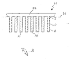
- the contour of the connector pins is first punched in a first punching step (solid line) of a metal strip 20 of eg CuFe 2 , wherein a one-sided transverse web 22 is maintained, which connects the plug pins at their first ends 9 together.
- the smooth cut portion at the first punching corresponds approximately to the fractional part, so that the plug pins must then be punched again in a fine stamping step (dashed line in Fig. 3) and now get their final contour.
- the smooth cut portion of the punched edges during the second punching is substantially higher, so that in particular the end surfaces 10 of the plug pins 7 provided as bonding surfaces receive a smooth, bondable surface structure.
- the Stekker be galvanically coated at least on the end faces 10 with a gold layer with nickel plating and separated along the line 21 in Fig. 3.
- the pins 7 are inserted into an injection mold and encapsulated except for the first ends 9 and the second ends 8 with an insulating material.
- the second ends 9 should not protrude more than 1 mm from the male part, in the case of thick wire bonding not more than 0.5 mm.
- the finished plug part 2 is fixed in a recess 5 of a support plate 1 such that the end faces 10 aligned at the second ends 8 of the plug pins 7 parallel to the pads 6 of the substrate 3 are. Subsequently, the pads 6 are connected to the end faces 10 via bonding wires 11 with a bonding tool.
Landscapes
- Engineering & Computer Science (AREA)
- Microelectronics & Electronic Packaging (AREA)
- Mechanical Engineering (AREA)
- Manufacturing & Machinery (AREA)
- Coupling Device And Connection With Printed Circuit (AREA)
- Manufacturing Of Electrical Connectors (AREA)
- Multi-Conductor Connections (AREA)
Abstract
Description
- Die Erfindung betrifft eine Anordnung mit den im Oberbegriff des Anspruchs 1 angegebenen Merkmalen und ein Verfahren nach Anspruch 6 zur Herstellung derselben. Die Merkmale des Oberbegriffs der Ansprüche 1 und 6 sind in
DE 43 08 898 C1 offenbart. - Eine derartige Anordnung ist bereits aus der
DE 42 40 755 A1 bekannt und wird insbesondere in elektronischen Steuergeräten verwandt. Die Anordnung umfaßt eine Trägerplatte mit einem aufgebrachten Leiterplattensubstrat, das mit einer elektronischen Schaltung und Bauelementen versehenen ist, und ein mit der Trägerplatte verbundenes Steckerteil mit mehreren in einem Isoliermaterial eingebetteten und beidseitig aus dem Steckerteil herausgeführten Steckerstiften. Die Anordnung wird z.B. in einem Kraftfahrzeug an externe Steckverbinder angeschlossen werden, die auf die ersten Enden der Steckerstifte aufsteckbar sind. Die der Leiterplatte zugewandten zweiten Enden der Steckerstifte verlaufen parallel zur Leiterplatte mit senkrecht zur Leiterplatte ausgerichteten Stirnflächen und sind an den gewalzten Seitenflächen über Bonddrähte mit Anschlußflächen auf der Leiterplatte verbunden. Nachteilig hierbei ist, daß bei einer derartigen Anordnung der Raum über den parallel zum Leiterplattensubstrat und der Trägerplatte ausgerichteten Seitenflächen der Steckerstifte freigehalten werden muß, damit das Bondwerkzeug bei der Herstellung der Bondverbindungen auf die Steckerstifte aufgesetzt werden kann. Eine Anordnung der Steckerstifte in mehreren parallelen Reihen ist deshalb nicht möglich, was insbesondere bei Steckerteilen mit sehr vielen Stiften dazu führt, daß die Steckerleiste seitlich erweitert werden muß, wodurch sich die räumlichen Abmessungen des Steckerteils nachteilig vergrößern und ein erheblicher Platzbedarf entsteht. Aufgrund der großen Entfernungen zu den weiter außen liegenden Steckerstiften werden außerdem lediglich Dickdrahtbondverbindung mit einem Drahtdurchmesser von 0,1 bis 0,3 mm auf die gewalzten Steitenflächen der Steckerstifte aufgebondet. Nachteilig hierbei ist, daß die Herstellung von Dickdraht-Bondverbindungen sehr viel mehr Zeit erfordert als die Herstellung von Dünndraht-Bondverbindungen. Darüber hinaus ist z.B. bei der Gehäusung von Hybridschaltkreisen bekannt, die Stirnseiten von Stekkerstiften mit Abkröpfungen oder Plateaus zu versehen, um direkt auf die Plateaus der Steckerstifte bonden zu können. Nachteilig hierbei ist, daß ein zusätzlicher aufwendiger Herstellungsschritt erforderlich ist, und das Steckerteil durch die räumliche Ausdehnung der Abkröpfungen insgesamt vergrößert wird. - Die erfindungsgemäße Anordnung mit dem Kennzeichen des Anspruchs 1 hat demgegenüber den Vorteil, daß der für den Anschluß des Substrats an die Steckerstifte benötigte Platzbedarf und die Breite des Steckerteils auf einfache Weise erheblich reduziert werden kann. Dies wird erreicht, indem die Bonddrähte direkt auf die fein gestanzten und parallel zum Substrat auf der Trägerplatte ausgerichteteten Stirnflächen der Steckerstifte aufgebondet werden. Die Abstände zwischen den als reine Stanzteile hergestellten Steckerstiften können vorteilhaft so klein gewählt werden, daß die Abmessungen des Rasters der Steckerstifte den Abmessungen des Rasters der Anschlußflächen auf dem Substrat entsprechen. Außerdem kann der Abstand zwischen den Steckerstiften und den Anschlußflächen des Substrats vorteilhaft verringert werden und die Substratgröße verkleinert werden. Hierdurch wird insgesamt eine kleiner, kompakter Aufbau der Anordnung realisiert.
- Insbesondere vorteilhaft ist, die Steckerstifte in mehreren parallelen Reihen im Steckerteil anzuordnen, da alle Stirnflächen der Steckerstifte frei zugänglich sind und das Bondwerkzeug bei der Herstellung der Bonddrahtverbindungen von der dem Substrat zugewandten Seite der Trägerplatte her auf die Stirnflächen aufgesetzt werden kann. Durch die Anordnung der Steckerstifte in mehreren parallelen Reihen wird vorteilhaft erreicht, daß die Breite des Rasters der Stirnflächen nicht größer ist als die Breite des Rasters der Anschlußflächen auf dem Substrat, auch dann wenn die Stirnflächen etwas breiter als die Anschlußflächen sind.
- Vorteilhaft ist weiterhin, zumindest die Stanzkanten der Steckerstifte mit einer galvanisch aufgebrachten Metallisierung zu beschichten, um die Qualität der Schweißverbindung zwischen Bonddraht und Steckerstift zu erhöhen.
- Vorteilhaft für die Herstellung des Steckerteils ist weiterhin, wenn die zweiten Enden der Steckerstifte ein Stück von dem als Spritzgußteil gefertigten Steckerteil abstehen, da dann die Steckerstifte während des Spritzgießen des Steckerteils mit großer Präzision im Spritzgußwerkzeug justiert gehalten werden können.
- Vorteilhaft ist außerdem das Steckerteil in einer Ausnehmung der Trägerplatte einzusetzten, da hierdurch die Steckerstifte auf besonders einfache Weise nahe an den Anschlußflächen des Substrats positioniert werden können.
- Vorteilhaft ist weiterhin ein Verfahren nach Anspruch 6 zur Herstellung einer Anordnung mit einer Trägerplatte und wenigstens einem darauf aufgebrachten Substrat für elektrische und/oder elektronische Bauelemente und mit einem Steckerteil mit mehreren in Isolierstoff eingebetteten Steckerstiften, deren erste Enden für den Anschluß externer Steckvorrichtungen vorgesehen sind und deren zweite Enden über Bonddrähte mit dem Substrat elektrisch verbunden sind, das folgende Schritte umfaßt: Freistanzen der Steckerstifte aus einem Metallband unter Beibehaltung eines einseitigen die Steckerstifte an ihren ersten Enden verbindenden Querstegs; Feinstanzen der Steckerstifte; Galvanisches Beschichten der Steckerstifte mit einer Kontaktmetallisierung; Entfernen des Querstegs; Einlegen der Steckerstifte in ein Spritzgießwerkzeug und Herstellung des Steckerteils durch Spritzgießen mit einem Isolierstoff; Einsetzen des Steckerteils in eine Ausnehmung der Trägerplatte mit in etwa parallel zu dem Substrat verlaufenden Stirnflächen der Steckerstifte und Herstellen von Bonddrahtverbindungen zwischen den Stirnflächen der einzelnen Steckerstifte und dem Substrat auf der Trägerplatte.
- Die Herstellung der Steckerstifte als einfache Stanzteile ist besonders kostengünstig. Durch das Feinstanzen der Stekkerstifte wird vorteilhaft erreicht, daß die Stirnflächen der Steckerstifte die zum Drahtbonden erforderliche Oberflächenqualität aufweisen. Die Steckerstifte werden dabei vorteilhaft über einen einseitigen Verbindungssteg gehalten, der erst nach der anschließenden galvanischen Beschichtung der Steckerstifte entfernt wird.
- Besonders vorteilhaft ist die Verwendung von Dünndrahtbondverbindungen mit einem Drahtdurchmesser von 0.025 bis 0.1 mm, deren Herstellung im Vergleich zu den im Stand der Technik üblichen Dickdrahtbondverbindungen sehr viel schneller durchgeführt werden kann.
- Ein Ausführungsbeispiel der Erfindung ist in der Zeichnung dargestellt und wird in der nachfolgenden Beschreibung näher erläutert. Es zeigt
- Fig. 1 einen Ausschnitt einem Querschnitt aus der erfindungsgemäßen Anordnung mit einem Trägerteil und einem Stekkerteil entlang der Linie I-I der Fig. 2,
- Fig. 2 einen Ausschnitt aus einer schematischen Draufsicht auf die erfindungsgemäße Anordnung mit einem Trägerteil und einem Steckerteil,
- Fig. 3 nach einem ersten Stanzvorgang durch einen einseitigen Quersteg miteinander verbundene Steckerstifte.
- Fig. 1 zeigt einen Querschnitt durch die erfindungsgemäße Anordnung, die z.B. in einem elektronischen Steuergerät eines Kraftfahrzeuges verwandt werden kann. Die Anordnung umfaßt eine Trägerplatte 1, die z.B. den Boden eines Steuergerätes bildet. Auf der Oberseite der Trägerplatte 1 befindet sich ein Substrat 3, das z.B. eine Leiterplatte, ein Hybridkeramiksubstrat oder ein Keramik-Multilayer sein kann. Das Substrat 3 umfaßt eine elektronische Schaltung mit Bauelementen 4, von denen nur eines in Fig. 1 und Fig. 2 gezeigt ist. Die Leiterbahnen, welche die Bauelemente 4 verbinden sind nicht dargestellt. Das Substrat 3 weist mit den Schaltungsteilen und den Bauelementen 4 verbundene Anschlußflächen 6 zum Anschluß an ein Steckerteil 2 auf, welches in einer Ausnehmung 5 der Trägerplatte 1 befestigt ist. Dies kann durch Schrauben, Kleben oder in anderer geeigneter Weise geschehen. Das Steckerteil 2 ist als Spritzgußteil ausgestaltet und weist mehrere in Isolierstoff eingebettete, als einfache Stanzteile hergestellte Steckerstifte 7 auf, die beidseitig aus dem Steckerteil 2 herausgeführt sind. Die Stekkerstifte können z.B. aus galvanisch mit Nickel und Gold beschichtetem CuFe2 hergestellt sein und weisen einen quadratischen Querschnitt von 0,6 x 0,6 mm auf. Die auf der dem Substrat 3 abgewandten Seite der Trägerplatte 1 aus dem Steckerteil 2 herausgeführten ersten Enden 9 der Steckerstifte 7 sind zum Anschluß an einen externen Gegenstecker vorgesehen, während die auf der dem Substrat zugewandten Oberseite der Trägerplatte 1 abstehenden zweiten Enden 8 zum elektrischen Anschluß an das Substrat 3 vorgesehen sind. Entscheidend ist, daß die Stirnflächen 10 an den zweiten Enden parallel zum Substrat 3 und den Anschlußflächen 6 ausgerichtet sind, damit das Bondwerkzeug an die Stirnflächen 10 und Anschlußflächen 6 herangeführt werden und eine Bonddrahtverbindung zwischen den Stirnflächen 10 und den Anschlußflächen 6 hergestellt werden kann. Die in Fig. 1 und Fig.2 dargestellten Bonddrähte 11, welche die Anschlußflächen 6 des Substrats 3 und die Stirnflächen 10 der Steckerstifte verbinden, können durch Dickdraht- oder Dünndrahtbonden hergestellt sein. Beim Dünndrahtbonden werden Golddrähte mit einem Durchmesser von 0,025 mm bis 0,1 mm verwandt, beim Dickdrahtbonden Aluminiumdrähte mit einem Durchmesser von 0,1 bis 0,3 mm. Die Steckerstifte 7 sind in zwei parallelen Reihen in dem Steckerteil 2 angeordnet. Es sind aber auch Ausführungen mit mehr als zwei Reihen denkbar. Wie insbesondere in Fig. 2 zu erkennen ist, sind die Steckerstifte 7 in dem Steckerteil 2 in zwei hintereinanderliegenden und versetzt zueinander liegenden Reihen angeordnet. Die Abmessungen des Rasters der Stirnflächen 10 korrespondieren zu dem Raster der Anschlußflächen 6 des Substrats 3 derart, daß die Breite des Rasters der Stirnflächen 10 nicht größer als die Breite des Rasters der Anschlußflächen 6 ist und daß sich die Anschlußflächen 6 und die Stirnflächen 10 gegenüberliegen. Hierduch werden die räumlichen Abmessungen der Anordnung vorteilhaft reduziert. Durch die versetzte Anordnung der beiden Reihen der Stirnflächen 10 wird dabei erreicht, daß die Bonddrähte zu den Stirnflächen 10 der weiter entfernt vom Substrat 3 angeordneten Reihe nicht die Stirnflächen 10 der näher am Substrat angeordneten vorderen Reihe überdecken, so daß eine Bonddrahtverbindung zu den vorderen Reihen problemlos hergestellt werden kann. Durch die Art der Anordnung sind die Stirnseiten 10 der Steckerstifte nahe an den Anschlußflächen 6 angeordnet, so daß die Bondverbindung zwischen den beidnen Flächen relativ kurz ist. Es kann daher sowohl mit Dickdraht als auch mit Dünndraht gebondet werden, wobei Dickdraht-Bondverbindungen insbesondere für hochstromige Anschlüsse verwandt werden.
- Im folgenden wird ein Verfahren zur Herstellung der oben beschriebenen Anordnung aufgezeigt. Wie in Fig. 3 dargestellt wird die Kontur der Steckerstifte zunächst in einem ersten Stanzschritt (durchgezogene Linie) aus einem Metallband 20 aus z.B. CuFe2 ausgestanzt, wobei ein einseitiger Quersteg 22 beibehalten wird, der die Steckerstifte an ihren ersten Enden 9 miteinander verbindet. Der Glattschnittanteil beim ersten Stanzen entspricht etwa dem Bruchanteil, so daß die Steckerstifte anschließend in einem Feinstanzschritt nochmals gestanzt werden müssen (gestrichelte Linie in Fig. 3) und nun ihre entgültige Kontur erhalten. Der Glattschnittanteil der Stanzkanten beim zweiten Stanzen ist wesentlich höher, so daß insbesondere die als Bondflächen vorgesehenen Stirnflächen 10 der Steckerstifte 7 eine glatte, bondfähige Oberflächenstruktur erhalten. Anschließend werden die Stekkerstifte zumindest an den Stirnflächen 10 galvanisch mit einer Goldschicht mit Unternickelung überzogen und entlang der Linie 21 in Fig. 3 vereinzelt. Die Stifte 7 werden in ein Spritzgußwerkzeug eingelegt und bis auf die ersten Enden 9 und die zweiten Enden 8 mit einem Isolierstoff umspritzt. Beim Dünndrahtbonden sollten die zweiten Enden 9 nicht mehr als 1 mm von dem Steckerteil abstehen, beim Dickdrahtbonden nicht mehr als 0,5 mm. Das fertige Steckerteil 2 wird in einer Ausnehmung 5 einer Trägerplatte 1 derart befestigt, daß die Stirnflächen 10 an den zweiten Enden 8 der Steckerstifte 7 parallel zu den Anschlußflächen 6 des Substrats 3 ausgerichtet sind. Anschließend werden die Anschlußflächen 6 mit den Stirnflächen 10 über Bondrähte 11 mit einem Bondwerkzeug verbunden.
Claims (7)
- Anordnung, insbesondere zur Verwendung in einem elektronischen Steuergerät, mit einer Trägerplatte (1) und wenigstens einem darauf aufgebrachten Substrat (3) für elektrische und/oder elektronische Bauelemente (4) und mit einem Steckerteil (2) mit mehreren in Isolierstoff eingebetteten Steckerstiften (7), deren erste Enden (9) für den Anschluß externer Steckvorrichtungen vorgesehen sind und deren zweite Enden (8) über Bonddrähte (11) mit dem Substrat (3) elektrisch verbunden sind,
wobei die einzelnen Steckerstifte (7) als Stanzteile hergestellt sind, dadurch gekennzeichnet, daß deren zumindest zweite Enden (8) jeweils eine in etwa parallel zu dem Substrat (3) verlaufende und durch einen Feinstanzvorgang hergestellte Stirnfläche (10) aufweisen, und daß die Bonddrähte (11) direkt auf die feingestanzten Stirnflächen (10) der Steckerstifte (7) aufgeschweißt sind. - Anordnung nach Anspruch 1, dadurch gekennzeichnet, daß die Steckerstifte (7) in wenigstens zwei Reihen in dem Steckerteil (2) angeordnet sind.
- Anordnung nach Anspruch 1, dadurch gekennzeichnet, daß die als Stanzteile hergestellten Steckerstifte (7) zumindest an den Stirnflächen (10) mit einer galvanisch aufgebrachten Metallisierung beschichtet sind.
- Anordnung nach Anspruch 1, dadurch gekennzeichnet, daß die zweiten Enden (8) der Steckerstifte (7) ein Stück von dem als Spritzgußteil gefertigten Steckerteil (2) abstehen.
- Anordnung nach Anspruch 1, dadurch gekennzeichnet, daß das Steckerteil (2) in einer Ausnehmung (5) der Trägerplatte (1) befestigt ist.
- Verfahren zur Herstellung einer Anordnung, insbesondere zur Verwendung in einem elektronischen Steuergerät, mit einer Trägerplatte (1) und wenigstens einem darauf aufgebrachten Substrat (3) für elektrische und/oder elektronische Bauelemente (4) und mit einem Steckerteil (2) mit mehreren in Isolierstoff eingebetteten Steckerstiften (7), deren erste Enden (9) für den Anschluß externer Steckvorrichtungen vorgesehen sind und deren zweite Enden (8) über Bonddrähte (11) mit dem Substrat (3) elektrisch verbunden sind, gekennzeichnet durch folgende Schritte:- Freistanzen der Steckerstifte (7) aus einem Metallband (20) unter Beibehaltung eines die Steckerstifte (7) an ihren ersten Enden (9) verbindenden Querstegs (22),- Feinstanzen der Steckerstifte (7), an den Stirnflächen (10) der zweiten Enden (8),- Galvanisches Beschichten zumindest der Stirnflächen (10) der Steckerstifte (7) mit einer Kontaktmetallisierung,- Entfernen des Querstegs (22),- Einlegen der Steckerstifte (7) in ein Spritzgießwerkzeug und Herstellung des Steckerteils (2) durch Spritzgießen mit einem isolierstoff,- Einsetzen des Steckerteils (2) in eine Ausnehmung (5) der Trägerplatte (1) mit in etwa parallel zu dem Substrat (3) verlaufenden Stirnflächen (10) der Steckerstifte (7) und- Herstellen von Bonddrahtverbindungen (11) zwischen den Stirnflächen (10) der einzelnen Steckerstifte (7) und dem Substrat (3) auf der Trägerplatte (1).
- Verfahren nach Anspruch 6, dadurch gekennzeichnet, daß zum Drahtbonden Dünndraht in einer Stärke von 0,025 bis 0,1 mm verwandt wird..
Applications Claiming Priority (3)
| Application Number | Priority Date | Filing Date | Title |
|---|---|---|---|
| DE19649549A DE19649549C1 (de) | 1996-11-29 | 1996-11-29 | Anordnung, insbesondere zur Verwendung in einem elektronischen Steuergerät, und Verfahren zur Herstellung derselben |
| DE19649549 | 1996-11-29 | ||
| PCT/DE1997/001810 WO1998024157A1 (de) | 1996-11-29 | 1997-08-22 | Anordnung, insbesondere zur verwendung in einem elektronischen steuergerät, und verfahren zur herstellung derselben |
Publications (2)
| Publication Number | Publication Date |
|---|---|
| EP0879492A1 EP0879492A1 (de) | 1998-11-25 |
| EP0879492B1 true EP0879492B1 (de) | 2007-11-21 |
Family
ID=7813160
Family Applications (1)
| Application Number | Title | Priority Date | Filing Date |
|---|---|---|---|
| EP97941804A Expired - Lifetime EP0879492B1 (de) | 1996-11-29 | 1997-08-22 | Anordnung, insbesondere zur verwendung in einem elektronischen steuergerät, und verfahren zur herstellung derselben |
Country Status (8)
| Country | Link |
|---|---|
| US (1) | US6304455B1 (de) |
| EP (1) | EP0879492B1 (de) |
| JP (1) | JP2000504478A (de) |
| KR (1) | KR100509665B1 (de) |
| CN (1) | CN1072850C (de) |
| DE (2) | DE19649549C1 (de) |
| RU (1) | RU2183892C2 (de) |
| WO (1) | WO1998024157A1 (de) |
Families Citing this family (18)
| Publication number | Priority date | Publication date | Assignee | Title |
|---|---|---|---|---|
| DE29819157U1 (de) | 1998-10-27 | 1999-01-07 | Siemens AG, 80333 München | Anschlußvorrichtung für eine elektronische Schaltung |
| DE10013090A1 (de) * | 2000-03-17 | 2001-09-20 | Boellhoff Gmbh | Flachstecker und Verfahren zu seiner Herstellung |
| JP2002134642A (ja) * | 2000-10-20 | 2002-05-10 | Keihin Corp | ワイヤボンディング端子構造 |
| US20080230282A1 (en) * | 2005-08-05 | 2008-09-25 | Weightech, Inc. | Modular sealed portable digital electronic controller |
| US7002084B2 (en) * | 2002-01-16 | 2006-02-21 | Weightech, Inc. | Modular sealed portable digital electronic controller |
| US20040089943A1 (en) * | 2002-11-07 | 2004-05-13 | Masato Kirigaya | Electronic control device and method for manufacturing the same |
| US7710714B2 (en) * | 2004-09-13 | 2010-05-04 | Bettcher Industries, Inc. | Housing for scale or load cell controller |
| USD548121S1 (en) | 2005-12-09 | 2007-08-07 | Bettcher Industries, Inc. | Housing for scale or load cell controller |
| EP2209172A1 (de) * | 2009-01-15 | 2010-07-21 | 3M Innovative Properties Company | Telekommunikationsbuchse mit einer Mehrschicht-Leiterplatte |
| RU2460170C1 (ru) * | 2011-05-06 | 2012-08-27 | Сергей Фёдорович Соболев | Способ изготовления электронного блока |
| US9362638B2 (en) * | 2014-09-03 | 2016-06-07 | Amphenol Corporation | Overmolded contact wafer and connector |
| DE102016205586A1 (de) * | 2016-04-05 | 2017-10-05 | Voith Patent Gmbh | Datenbusstecker für hohe Datenraten |
| CN106025769B (zh) | 2016-07-27 | 2018-09-11 | 广东欧珀移动通信有限公司 | 电源适配器、移动终端及电源接口的制造方法 |
| WO2018018948A1 (zh) * | 2016-07-27 | 2018-02-01 | 广东欧珀移动通信有限公司 | 移动终端、电源适配器、电源接口及制造方法 |
| CN106099459A (zh) * | 2016-07-27 | 2016-11-09 | 广东欧珀移动通信有限公司 | 移动终端、电源适配器、电源接口及制造方法 |
| US12355000B2 (en) | 2020-11-10 | 2025-07-08 | Qualcomm Incorporated | Package comprising a substrate and a high-density interconnect integrated device |
| US12469811B2 (en) * | 2021-03-26 | 2025-11-11 | Qualcomm Incorporated | Package comprising wire bonds coupled to integrated devices |
| DE102022203012A1 (de) * | 2022-03-28 | 2023-09-28 | New Ventures GmbH | Verfahren zur Herstellung einer Baugruppe für ein Patienten-Beatmungssystem |
Citations (1)
| Publication number | Priority date | Publication date | Assignee | Title |
|---|---|---|---|---|
| DE4308898C1 (de) * | 1993-03-19 | 1994-03-17 | Siemens Nixdorf Inf Syst | Druckkopf für eine elektrografische Druckeinrichtung |
Family Cites Families (16)
| Publication number | Priority date | Publication date | Assignee | Title |
|---|---|---|---|---|
| DE2732087A1 (de) * | 1977-07-15 | 1979-01-25 | Siemens Ag | Loesbare und nichtloesbare elektrische kontakte |
| US4484158A (en) * | 1982-07-07 | 1984-11-20 | General Electric Company | Monolithic crystal filter and method of manufacturing same |
| FR2620296B1 (fr) * | 1987-09-03 | 1990-01-19 | Bendix Electronics Sa | Boitier pour circuit electronique |
| JPH01163985A (ja) * | 1987-12-02 | 1989-06-28 | Yazaki Corp | インサート端子の製造方法およびインサート端子製造用端子板 |
| JPH0266865A (ja) | 1988-08-31 | 1990-03-06 | Nec Corp | コネクタの製造方法 |
| DE69227066T2 (de) * | 1991-05-31 | 1999-06-10 | Denso Corp., Kariya, Aichi | Elektronische Vorrichtung |
| DE4142138C2 (de) * | 1991-12-20 | 1998-04-23 | Bosch Gmbh Robert | Elektrisches Steuergerät |
| RU2035281C1 (ru) * | 1992-02-14 | 1995-05-20 | Научно-исследовательский институт "Пульсар" | Способ присоединения выводов к контактным площадкам и устройство для его осуществления |
| US5263880A (en) * | 1992-07-17 | 1993-11-23 | Delco Electronics Corporation | Wirebond pin-plastic header combination and methods of making and using the same |
| DE4240755A1 (de) * | 1992-12-03 | 1994-06-16 | Siemens Ag | Steuergerät, insbesondere für ein Kraftfahrzeug |
| US5359761A (en) * | 1993-09-09 | 1994-11-01 | Delco Electronics Corp. | Method of making a header or housing for electrical connection to a hybrid circuit including an in-cavity trim of a terminal frame |
| JP3198779B2 (ja) * | 1994-03-04 | 2001-08-13 | 株式会社デンソー | 半導体圧力検出器の製造方法 |
| DE4426465A1 (de) * | 1994-07-26 | 1996-02-01 | Siemens Ag | Verbindungsteil zwischen elektrischen Anschlüssen im Inneren eines Gehäuses und aus dem Gehäuse herausragenden Anschlüssen |
| US5530287A (en) * | 1994-09-14 | 1996-06-25 | Unisys Corporation | High density wire bond pattern for integratd circuit package |
| US5668698A (en) * | 1996-01-22 | 1997-09-16 | General Motors Corporation | Smart connector for an electrical device |
| US5774342A (en) * | 1996-09-26 | 1998-06-30 | Delco Electronics Corporation | Electronic circuit with integrated terminal pins |
-
1996
- 1996-11-29 DE DE19649549A patent/DE19649549C1/de not_active Expired - Fee Related
-
1997
- 1997-08-22 US US09/117,466 patent/US6304455B1/en not_active Expired - Fee Related
- 1997-08-22 DE DE59712896T patent/DE59712896D1/de not_active Expired - Fee Related
- 1997-08-22 WO PCT/DE1997/001810 patent/WO1998024157A1/de not_active Ceased
- 1997-08-22 CN CN97191812A patent/CN1072850C/zh not_active Expired - Fee Related
- 1997-08-22 RU RU98116066/09A patent/RU2183892C2/ru not_active IP Right Cessation
- 1997-08-22 EP EP97941804A patent/EP0879492B1/de not_active Expired - Lifetime
- 1997-08-22 JP JP10524110A patent/JP2000504478A/ja active Pending
- 1997-08-22 KR KR10-1998-0705768A patent/KR100509665B1/ko not_active Expired - Fee Related
Patent Citations (1)
| Publication number | Priority date | Publication date | Assignee | Title |
|---|---|---|---|---|
| DE4308898C1 (de) * | 1993-03-19 | 1994-03-17 | Siemens Nixdorf Inf Syst | Druckkopf für eine elektrografische Druckeinrichtung |
Also Published As
| Publication number | Publication date |
|---|---|
| RU2183892C2 (ru) | 2002-06-20 |
| KR19990082048A (ko) | 1999-11-15 |
| JP2000504478A (ja) | 2000-04-11 |
| DE59712896D1 (de) | 2008-01-03 |
| KR100509665B1 (ko) | 2005-11-08 |
| CN1072850C (zh) | 2001-10-10 |
| US6304455B1 (en) | 2001-10-16 |
| CN1209910A (zh) | 1999-03-03 |
| DE19649549C1 (de) | 1998-04-09 |
| WO1998024157A1 (de) | 1998-06-04 |
| EP0879492A1 (de) | 1998-11-25 |
Similar Documents
| Publication | Publication Date | Title |
|---|---|---|
| DE19649549C1 (de) | Anordnung, insbesondere zur Verwendung in einem elektronischen Steuergerät, und Verfahren zur Herstellung derselben | |
| DE68917694T2 (de) | Schaltungsplattenzusammenbau und Kontaktstift, der darin verwendet wird. | |
| DE69530103T2 (de) | Verbindungselemente für mikroelektronische komponenten | |
| EP0639884B1 (de) | Verfahren zur Herstellung einer elektrischen Antriebseinheit | |
| EP1484511B1 (de) | Verkettungsmodul zur Ansteuerung eines elektrischen Ventilantriebs einer fluidtechnischen Ventilanordnung | |
| EP0863530A2 (de) | Leiterplatte für elektrische Schaltungen und Verfahren zur Herstellung einer solchen Leiterplatte | |
| EP0929428B1 (de) | Ventilsteuergerät mit dreidimensionaler leiterplatte in mid-technik | |
| DE4244064A1 (de) | Einrichtung für ein Fahrzeug | |
| EP1128476B1 (de) | Steckverbinder sowie Verfahren zur Herstellung eines Steckverbinders | |
| EP1165354A1 (de) | Anordnung zur kontaktierung eines elektrischen bauteils mit einer elektrischen schaltung | |
| DE102015109333A1 (de) | Optoelektronisches Bauelement | |
| DE102008058003A1 (de) | Halbleitermodul und Verfahren zu dessen Herstellung | |
| EP1791178B1 (de) | Leistungshalbleitermodul in Druckkontaktausführung | |
| EP0811995A1 (de) | Magnetspule sowie Verfahren zu deren Herstellung | |
| EP2514286B1 (de) | Steuergerät für ein kraftfahrzeug und zugehöriges verfahren zur montage eines steuergeräts für ein kraftfahrzeug | |
| DE10038390C1 (de) | Funktionell asymmetrische Schaltungsträgeranordnung mit spiegelsymmetrischer Bauteileanordnung | |
| WO1996010280A1 (de) | Steckverbinder mit einer stiftkontaktleiste und einer buchsenkontaktleiste | |
| DE102006009582B4 (de) | Elektronisches Gerät eines Fahrzeuges, insbesondere ein Antennenverstärker oder ein TV-Tuner, mit einem Aufnahmeraum für einen Steckverbinder | |
| DE102006030081A1 (de) | Sensor mit Leadframe und Herstellungsverfahren hierfür | |
| DE4136031C1 (en) | Double plug contact for car electric installation - consists of 2 terminal contact fins integral with strip conductor web | |
| EP2232219A1 (de) | Leiterbahnträger sowie verfahren zur herstellung eines leiterbahnträgers | |
| DE102007037841A1 (de) | Trägermodul und Verfahren zur Herstellung eines Trägermoduls | |
| DE4422857C2 (de) | Schaltvorrichtung und Verfahren zur Herstellung einer Sockelplatteneinheit hierfür | |
| EP0959528B1 (de) | Vorrichtung zur Herstellung einer Crimpverbindung | |
| DE102024202558A1 (de) | Kontaktieranordnung für zwei räumlich getrennte elektrische Komponenten |
Legal Events
| Date | Code | Title | Description |
|---|---|---|---|
| PUAI | Public reference made under article 153(3) epc to a published international application that has entered the european phase |
Free format text: ORIGINAL CODE: 0009012 |
|
| AK | Designated contracting states |
Kind code of ref document: A1 Designated state(s): DE FR GB IT |
|
| 17P | Request for examination filed |
Effective date: 19981204 |
|
| 17Q | First examination report despatched |
Effective date: 20051025 |
|
| GRAP | Despatch of communication of intention to grant a patent |
Free format text: ORIGINAL CODE: EPIDOSNIGR1 |
|
| GRAS | Grant fee paid |
Free format text: ORIGINAL CODE: EPIDOSNIGR3 |
|
| GRAA | (expected) grant |
Free format text: ORIGINAL CODE: 0009210 |
|
| AK | Designated contracting states |
Kind code of ref document: B1 Designated state(s): DE FR GB IT |
|
| REG | Reference to a national code |
Ref country code: GB Ref legal event code: FG4D Free format text: NOT ENGLISH |
|
| REF | Corresponds to: |
Ref document number: 59712896 Country of ref document: DE Date of ref document: 20080103 Kind code of ref document: P |
|
| GBT | Gb: translation of ep patent filed (gb section 77(6)(a)/1977) |
Effective date: 20080227 |
|
| ET | Fr: translation filed | ||
| PLBE | No opposition filed within time limit |
Free format text: ORIGINAL CODE: 0009261 |
|
| STAA | Information on the status of an ep patent application or granted ep patent |
Free format text: STATUS: NO OPPOSITION FILED WITHIN TIME LIMIT |
|
| 26N | No opposition filed |
Effective date: 20080822 |
|
| PGFP | Annual fee paid to national office [announced via postgrant information from national office to epo] |
Ref country code: IT Payment date: 20080826 Year of fee payment: 12 Ref country code: FR Payment date: 20080818 Year of fee payment: 12 |
|
| PGFP | Annual fee paid to national office [announced via postgrant information from national office to epo] |
Ref country code: GB Payment date: 20080822 Year of fee payment: 12 |
|
| PGFP | Annual fee paid to national office [announced via postgrant information from national office to epo] |
Ref country code: DE Payment date: 20081024 Year of fee payment: 12 |
|
| GBPC | Gb: european patent ceased through non-payment of renewal fee |
Effective date: 20090822 |
|
| REG | Reference to a national code |
Ref country code: FR Ref legal event code: ST Effective date: 20100430 |
|
| PG25 | Lapsed in a contracting state [announced via postgrant information from national office to epo] |
Ref country code: FR Free format text: LAPSE BECAUSE OF NON-PAYMENT OF DUE FEES Effective date: 20090831 Ref country code: DE Free format text: LAPSE BECAUSE OF NON-PAYMENT OF DUE FEES Effective date: 20100302 |
|
| PG25 | Lapsed in a contracting state [announced via postgrant information from national office to epo] |
Ref country code: GB Free format text: LAPSE BECAUSE OF NON-PAYMENT OF DUE FEES Effective date: 20090822 |
|
| PG25 | Lapsed in a contracting state [announced via postgrant information from national office to epo] |
Ref country code: IT Free format text: LAPSE BECAUSE OF NON-PAYMENT OF DUE FEES Effective date: 20090822 |