EP0873811A1 - Position correction apparatus for laser marker - Google Patents
Position correction apparatus for laser marker Download PDFInfo
- Publication number
- EP0873811A1 EP0873811A1 EP96906919A EP96906919A EP0873811A1 EP 0873811 A1 EP0873811 A1 EP 0873811A1 EP 96906919 A EP96906919 A EP 96906919A EP 96906919 A EP96906919 A EP 96906919A EP 0873811 A1 EP0873811 A1 EP 0873811A1
- Authority
- EP
- European Patent Office
- Prior art keywords
- lens
- marking
- movement distance
- marking position
- onto
- Prior art date
- Legal status (The legal status is an assumption and is not a legal conclusion. Google has not performed a legal analysis and makes no representation as to the accuracy of the status listed.)
- Withdrawn
Links
- 239000003550 marker Substances 0.000 title claims abstract description 21
- 238000012937 correction Methods 0.000 title claims description 8
- 238000013461 design Methods 0.000 claims abstract description 23
- 238000004519 manufacturing process Methods 0.000 claims abstract description 12
- 239000004973 liquid crystal related substance Substances 0.000 claims description 27
- 230000001678 irradiating effect Effects 0.000 claims description 5
- 230000003287 optical effect Effects 0.000 claims description 2
- 238000000034 method Methods 0.000 description 8
- 230000000694 effects Effects 0.000 description 6
- 238000012545 processing Methods 0.000 description 5
- 238000010586 diagram Methods 0.000 description 4
- 238000010330 laser marking Methods 0.000 description 4
- 230000009467 reduction Effects 0.000 description 3
- 230000015572 biosynthetic process Effects 0.000 description 2
- 239000013256 coordination polymer Substances 0.000 description 2
- 238000011835 investigation Methods 0.000 description 1
- 238000005259 measurement Methods 0.000 description 1
- 230000010355 oscillation Effects 0.000 description 1
- 230000004044 response Effects 0.000 description 1
Images


Classifications
-
- B—PERFORMING OPERATIONS; TRANSPORTING
- B23—MACHINE TOOLS; METAL-WORKING NOT OTHERWISE PROVIDED FOR
- B23K—SOLDERING OR UNSOLDERING; WELDING; CLADDING OR PLATING BY SOLDERING OR WELDING; CUTTING BY APPLYING HEAT LOCALLY, e.g. FLAME CUTTING; WORKING BY LASER BEAM
- B23K26/00—Working by laser beam, e.g. welding, cutting or boring
- B23K26/02—Positioning or observing the workpiece, e.g. with respect to the point of impact; Aligning, aiming or focusing the laser beam
- B23K26/06—Shaping the laser beam, e.g. by masks or multi-focusing
- B23K26/064—Shaping the laser beam, e.g. by masks or multi-focusing by means of optical elements, e.g. lenses, mirrors or prisms
- B23K26/066—Shaping the laser beam, e.g. by masks or multi-focusing by means of optical elements, e.g. lenses, mirrors or prisms by using masks
-
- B—PERFORMING OPERATIONS; TRANSPORTING
- B23—MACHINE TOOLS; METAL-WORKING NOT OTHERWISE PROVIDED FOR
- B23K—SOLDERING OR UNSOLDERING; WELDING; CLADDING OR PLATING BY SOLDERING OR WELDING; CUTTING BY APPLYING HEAT LOCALLY, e.g. FLAME CUTTING; WORKING BY LASER BEAM
- B23K26/00—Working by laser beam, e.g. welding, cutting or boring
- B23K26/02—Positioning or observing the workpiece, e.g. with respect to the point of impact; Aligning, aiming or focusing the laser beam
- B23K26/06—Shaping the laser beam, e.g. by masks or multi-focusing
- B23K26/064—Shaping the laser beam, e.g. by masks or multi-focusing by means of optical elements, e.g. lenses, mirrors or prisms
Definitions
- the present invention relates to a device for correcting a marking position of a laser marker.
- a device whereby a desired pattern is marked onto a specimen by irradiating the specimen with laser light is disclosed in Japanese Patent Publication 4-39646 .
- reference marks are provided at prescribed intervals in the X direction at the specimen stage, photodetector elements are provided, laser light is scanned in the X direction prior to actual marking, the divergence ⁇ X from the reference mark is determined for each reference mark from the timing at which light is received at each photodetector element, and the position of laser irradiation in the X direction is corrected for each reference mark on the basis of the divergence ⁇ X for each reference mark.
- the present invention was devised in view of the foregoing, its object being to provide a laser marker wherein the marking position can be corrected by means of a simple calculational process using a small quantity of corrective data, thereby enabling reductions in cost and increases in speed to be achieved.
- a marking position correction device for a laser marker which comprises: display means for dividing a marking pattern of an original image which is to be marked onto an object into marking patterns of divided images, and displaying the marking patterns of the divided images on a liquid crystal display screen; optical means for irradiating laser light generated by a laser light source onto the liquid crystal display screen and irradiating light which has permeated the liquid crystal display screen through a lens onto the object; lens moving means for moving the lens by a movement distance corresponding to a movement command signal, so as to mark the marking pattern of the divided image displayed on the liquid crystal display screen onto a position on the object corresponding to the movement distance; and control means for calculating the movement distance of the lens for marking the marking pattern of the divided image onto a desired position on the object corresponding to the divided image on the basis of a design parameter of
- a movement command signal corresponding to this lens movement distance ⁇ should be supplied to the lens moving means.
- the aforementioned corrective value ⁇ is a uniform data value based on a production tolerance, d ⁇ , determined uniformly according to the lens used, and since the design parameter is corrected by a simple calculational process using only a uniform corrective value, ⁇ , the marking position can be corrected at low cost and at high speed.
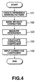
- Fig. 1 is an oblique view showing the composition of a laser marker according to the embodiment.
- this device comprises: a host computer 50 which inputs data relating to an original image to be marked onto the marking surface of a work 9 and creates original image data; a panel controller 60 which converts original image data output from the aforementioned host computer 50 to marking pattern data for a divided image of smaller blocks; a marker controller 70 which sends marking pattern data for a divided image output from the aforementioned panel controller 60 to a liquid crystal mask 6, and drives and controls a drive system of the laser marker; and a laser marking device (optics system and drive system) which directs laser light generated by a laser oscillator 1 onto the marking surface of the work 9.
- a host computer 50 which inputs data relating to an original image to be marked onto the marking surface of a work 9 and creates original image data
- a panel controller 60 which converts original image data output from the aforementioned host computer 50 to marking pattern data for a divided image of smaller blocks
- the laser marking device in Fig. 1 conducts raster scanning of the laser light L0 over the display screen of a liquid crystal mask 6, and the laser light L transmitted thereby is deflected and directed onto the work 9 by means of a second XY deflector (hereinafter, called an "XY table" for the sake of convenience,) whereby the marking pattern displayed on the liquid crystal mask 6 is marked onto the work 9.
- a second XY deflector hereinafter, called an "XY table" for the sake of convenience
- laser light L0 generated by the laser oscillator 1 passes through a beam splitter 2 and is caused to oscillate in the Y direction (vertical direction of the liquid crystal mask 6 in the diagram) by means of a galvanoscanner meter 3Y.
- the laser light L0 is condensed by a relay lens 4 and is caused to oscillate in the X direction (horizontal direction of the liquid crystal mask 6 in the diagram) by means of a polygon mirror 3X.
- the laser light L0 is then caused to converge on a reflecting mirror 7 by means of a lens 5.
- the laser light L0 is raster scanned over the divided pattern display screen on the liquid crystal mask 6 in response to the movement of the aforementioned galvanoscanner meter 3Y and polygon mirror 3X.
- the laser light L transmitted by the divided pattern display screen passes through an object lens 8 and enters the second XY deflector.
- the marking pattern of the divided image on the liquid crystal mask 6 is deflected and directed by the second deflector onto a corresponding marking position.
- the second XY deflector comprises a first XY table 10, a second XY table 20, and a base 30 supported by these tables 10, 20 and having a lens 40.
- the first XY table 10 is driven in the X direction by means of a drive motor 11, and the second XY table 20 is also driven in the X direction in accordance with the movement of this first XY table 10. Meanwhile, the second XY table 20 is driven in the Y direction by a drive motor 21 and the first XY table 10 is also driven in the Y direction in accordance with the movement of the second XY table 20.
- the motors 11 and 21 are pulse motors, for example, and the irradiation point P on the marking surface of the work 9 is moved by a predetermined distance for each pulse.
- the lens 40 in the center of the base 30 is moved by an amount of lens movement, ⁇ X and ⁇ Y, respectively, in the X and Y directions, and the laser light L transmitted by the lens 40 is moved by a movement distance ⁇ 'X, ⁇ 'Y corresponding to the aforementioned amount of lens movement ⁇ X, ⁇ Y over the XY plane of the work 9. Therefore, the laser light L is focused and directed onto a position P corresponding to the movement distances ⁇ 'X, ⁇ 'Y, and the marking pattern on the liquid crystal mask 6 is marked onto the position P.
- marking patterns of a divided image (small block) 81 are successively marked onto the marking surface of a work 9 as indicated by the arrows, and finally a marking pattern of the entire original image 80 is marked onto a square region having sides 55 mm long.
- the size of the marking region may be 40 ⁇ 60 mm, 60 ⁇ 40 mm, 70 ⁇ 30 mm, 30 ⁇ 70 mm, and it can be set as desired.
- the oscillation of the laser oscillator 1, the driving of the first XY deflector 3X, 3Y, the driving of the second XY deflector, the display switching of each divided pattern on the liquid crystal mask 6, and the like, are controlled by the marker controller 70.
- the host computer 50 As well as the original image data to be printed onto the marking surface of the work 9, the host computer 50 generates data for the coordinates position to be marked in ⁇ m units, and this data is transferred to the panel controller 60.
- the panel controller 60 receives the aforementioned data and records it in a memory, and then records a code number indicating the original image transmitted from the host computer 50.
- the received original image data is converted to a marking pattern (data for liquid crystal display) for each divided image.
- the marking position data data for the movement distance ⁇ ' up to the marking position
- the panel controller 60 converts the unit of this data to a number of command pulses (in both the X direction and Y direction) for supply to the pulse motors 11, 21.
- the marking position movement distance ⁇ ' ( ⁇ 'X, ⁇ 'Y) converted to the aforementioned unit is then converted to the aforementioned lens movement distance ⁇ ( ⁇ X, ⁇ Y).
- data for the lens movement distance ⁇ (number of pulses corresponding to the size of movement distance) is obtained.
- data for the lens movement distance ⁇ in the form of a number of pulses corresponding to the size of the movement distance is output to the marker controller 70, along with data for the printing pattern of the aforementioned divided image.
- the marker controller 70 generates a pulse signal containing a number of pulses corresponding to the size of the movement distance on the basis of the data for the lens movement distance ⁇ , and it outputs this as a movement command signal to the motors 11, 21.
- the marker controller 70 also converts the data for the marking pattern of a divided image (data for liquid crystal display) to an electrode supply signal for the electrodes of the liquid crystal 6, this electrode supply signal is fed to the liquid crystal mask 6, and a marking pattern is displayed on the liquid crystal mask 6.
- composition of the laser marker is not limited to that described above and it may be changed as appropriate.
- the whole surface of the liquid crystal mask 6 may be irradiated by laser light.
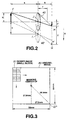
- Fig. 2 is a diagram for describing the geometrical relationship when the lens 40 is moved in a plane perpendicular to the paper surface (this is assumed to be plane X-Y in Fig. 1). The vertical direction of the paper surface is taken as the X axis.
- the lens 40 is then moved by the movement distance ⁇ in the plus direction of the X axis, and the center of the lens is positioned at point I.
- the image is formed at a point G on the image formation surface which is shifted by the movement distance ⁇ ' in the plus direction of the X axis.
- the movement distance of the image formation position namely, the marking position movement distance ⁇ '
- the marking position movement distance ⁇ ' is a magnification of (1 + ⁇ ) of the lens movement distance ⁇ .
- the first item on the right-hand side of equation (3) indicates that the tolerance d ⁇ of the lens magnification factor has an effect on the divergence in marking position, and the second element on the right-hand side indicates that the lens locating precision d ⁇ has an effect on the divergence in marking position.
- a case is supposed where a square region having sides 55 mm long is marked.
- the lens magnification factor ⁇ is 1.4
- the tolerance of lens magnification factor d ⁇ is ⁇ 0.01
- the lens locating precision d ⁇ is ⁇ 5 ⁇ m.
- the tolerance d ⁇ of lens magnification factor differs for each individual lens produced, and a uniform value for d ⁇ is set for each lens. Therefore, it can be seen that, if the tolerance d ⁇ is calculated beforehand for a lens as described below, then as demonstrated by equation (4), the divergence in the marking position d ⁇ ' can be corrected universally for a desired marking position.
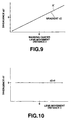
- Equation (4) d ⁇ ' ⁇ d ⁇ ⁇ ⁇ , indicates that there is a proportional relationship between the lens movement distance ⁇ and the divergence in marking position d ⁇ ', and that the proportional constant is the tolerance d ⁇ of lens magnification factor.
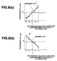
- a proportional relationship K as shown in Fig. 9 is determined by the minimum square rule, or the like, and the tolerance d ⁇ of lens magnification factor is determined from the gradient of K.
- the origin O on the vertical axis indicates a case where there is zero divergence between the desired marking position and the actual marking position.
- the designed value for the magnification factor of the lens 40 is taken as ⁇ , and the measured value for the magnification factor of the lens 40 when it is actually produced is taken as ⁇ '.
- the lens movement distance ⁇ ( ⁇ m) can be calculated by substituting the marking position movement distance ⁇ ' ( ⁇ m) corresponding to the desired marking position, the lens design value ⁇ , and the corrective coefficient ⁇ into equation (9). Thereupon, a movement command signal containing a number of pulses for moving the lens 40 by this lens movement distance ⁇ is generated, and by outputting this signal to the aforementioned pulse motors 11, 21, the laser marking position can be corrected such that it moves to the desired marking position.
- the host computer 50 generates an original image containing a plurality of reference marking patterns PT as shown in Fig. 5(a).
- This original image of reference marking patterns PT is divided by the panel controller 60 into divided images 81 containing a single reference marking pattern.
- the marking positions for each reference marking pattern PT, A-1 (-27, 27), B-1 (-13.5, 27), ... are set beforehand, and C-3 is taken as the point of origin (0,0).
- the reference marking pattern PT is constituted by dots as illustrated in Fig. 5(b) (step 101).
- the divided images 81 in Fig. 5(a) are displayed on the liquid crystal mask 6.
- Laser light L0 is generated by a laser oscillator 1 and the reference marking pattern transmitted by the liquid crystal mask 6 is marked onto the marking surface of a work 9 via a lens 40.
- a movement command signal obtained on the basis of equation (7) is supplied to the pulse motors 11, 21 which drive the XY tables 10, 20, and the XY tables 10, 20 move in the X and Y directions.
- the reference marking pattern PT is actually marked in a position P which diverges from the set marking position Pr (for example, point A-1) (step 102).
- This divergence in the marking position d ⁇ ' is measured in both the X direction and Y direction.
- the divergence in the marking position in the X direction, d ⁇ 'X is measured for each of the set marking positions A-1, A-2, ... of the reference marking pattern PT, as shown in Fig. 7(a).
- the averages for points A, B, C, D, E are then found.
- the divergence in the marking position in the Y direction, d ⁇ 'Y is measured for each of the set marking positions 1-A, 1-B, ... of the reference marking pattern PT, as shown in Fig. 7(b).
- the averages for points 1, 2, 3, 4, 5 are then found (step 103).
- the average divergence d ⁇ 'X for each of the points A, B, C, D, E in Fig. 7(a) is plotted on the vertical axis with respect to the set marking values A, B, C, D, E in the X direction, and a proportional relationship L is derived by means of the minimum square rule.
- the horizontal axis shows the lens movement distance in the X direction, ⁇ X.
- the average divergence d ⁇ 'Y for each of the points 1, 2, 3, 4, 5 in Fig. 7(b) are plotted on the vertical axis with respect to the set marking values in the Y direction, and a proportional relationship M is derived by means of the minimum square rule.
- the horizontal axis shows the lens movement distance in the Y direction, ⁇ Y.
- the corrective coefficient ⁇ can be derived from equation (5) and equation (6) (step 104).
- the corrective coefficient ⁇ is substituted into equation (9) and the lens magnification factor is corrected by the degree of tolerance d ⁇ .
- the lens movement distance ⁇ ( ⁇ m) is calculated.
- a movement command signal containing a number of pulses for moving the lens 40 by this calculated lens movement distance ⁇ is generated and this signal is output to the aforementioned motor 11, 21. Consequently, a marking pattern of a divided image 81 is marked onto a desired marking position.
- the marking position was corrected on the basis of production tolerance in the magnification factor of the lens 40, but it may also be corrected by a similar method on the basis of production tolerance in design parameters other than the lens magnification factor.
Landscapes
- Physics & Mathematics (AREA)
- Optics & Photonics (AREA)
- Engineering & Computer Science (AREA)
- Plasma & Fusion (AREA)
- Mechanical Engineering (AREA)
- Laser Beam Processing (AREA)
- Manufacture Or Reproduction Of Printing Formes (AREA)
Applications Claiming Priority (3)
| Application Number | Priority Date | Filing Date | Title |
|---|---|---|---|
| JP06286195A JP3413645B2 (ja) | 1995-03-22 | 1995-03-22 | レーザ刻印装置における刻印位置補正装置 |
| JP62861/95 | 1995-03-22 | ||
| PCT/JP1996/000747 WO1996029175A1 (en) | 1995-03-22 | 1996-03-22 | Position correction apparatus for laser marker |
Publications (2)
| Publication Number | Publication Date |
|---|---|
| EP0873811A4 EP0873811A4 (enExample) | 1998-10-28 |
| EP0873811A1 true EP0873811A1 (en) | 1998-10-28 |
Family
ID=13212509
Family Applications (1)
| Application Number | Title | Priority Date | Filing Date |
|---|---|---|---|
| EP96906919A Withdrawn EP0873811A1 (en) | 1995-03-22 | 1996-03-22 | Position correction apparatus for laser marker |
Country Status (5)
| Country | Link |
|---|---|
| US (1) | US5896233A (enExample) |
| EP (1) | EP0873811A1 (enExample) |
| JP (1) | JP3413645B2 (enExample) |
| KR (1) | KR960033640A (enExample) |
| WO (1) | WO1996029175A1 (enExample) |
Cited By (1)
| Publication number | Priority date | Publication date | Assignee | Title |
|---|---|---|---|---|
| FR2821678A1 (fr) * | 2001-03-02 | 2002-09-06 | Teem Photonics | Module de deflexion optique |
Families Citing this family (8)
| Publication number | Priority date | Publication date | Assignee | Title |
|---|---|---|---|---|
| JPH09277069A (ja) * | 1996-04-12 | 1997-10-28 | Komatsu Ltd | 液晶マスク、液晶式レーザマーカ及びそれを用いた刻印方法 |
| US20040241340A1 (en) * | 2001-10-25 | 2004-12-02 | Kenji Sato | Method and device for marking identification code by laser beam |
| US7476629B2 (en) * | 2003-04-21 | 2009-01-13 | Semiconductor Energy Laboratory Co., Ltd. | Beam irradiation apparatus, beam irradiation method, and method for manufacturing thin film transistor |
| US7220627B2 (en) * | 2003-04-21 | 2007-05-22 | Semiconductor Energy Laboratory Co., Ltd. | Method for manufacturing a semiconductor device where the scanning direction changes between regions during crystallization and process |
| US7397592B2 (en) * | 2003-04-21 | 2008-07-08 | Semiconductor Energy Laboratory Co., Ltd. | Beam irradiation apparatus, beam irradiation method, and method for manufacturing a thin film transistor |
| WO2007069516A1 (en) * | 2005-12-16 | 2007-06-21 | Semiconductor Energy Laboratory Co., Ltd. | Laser irradiation apparatus, laser irradiation method, and manufacturing method of semiconductor device |
| US9018561B2 (en) * | 2007-05-23 | 2015-04-28 | Cymer, Llc | High power seed/amplifier laser system with beam shaping intermediate the seed and amplifier |
| CN102248817B (zh) * | 2010-05-21 | 2013-07-03 | 深圳泰德激光科技有限公司 | 激光打标的校正方法和校正装置以及激光打标系统 |
Family Cites Families (11)
| Publication number | Priority date | Publication date | Assignee | Title |
|---|---|---|---|---|
| US4045201A (en) * | 1976-07-09 | 1977-08-30 | American Atomics Corporation | Method and apparatus for subdividing a gas filled glass tube |
| JPS6046978A (ja) * | 1983-08-20 | 1985-03-14 | 長尾曹達株式会社 | セラミック多孔体の製造患法 |
| JPS6046978U (ja) * | 1983-09-05 | 1985-04-02 | 渋谷工業株式会社 | レ−ザ光線の加工位置移動装置 |
| JPH01228688A (ja) * | 1988-03-09 | 1989-09-12 | Mitsubishi Electric Corp | レーザ加工機の加工ヘッド |
| JP2840103B2 (ja) * | 1990-02-26 | 1998-12-24 | 川崎製鉄株式会社 | 高クロム含有圧延用素材鋼の製造方法 |
| JPH03248784A (ja) * | 1990-02-28 | 1991-11-06 | Hitachi Ltd | レーザマーキングシステム |
| KR950013780B1 (ko) * | 1990-05-22 | 1995-11-16 | 후루까와 뗀끼 고요교오 가부시끼가이샤 | 이동하고 있는 길다란 물건의 길이를 측정하는 장치 및 그 방법 |
| JPH0439646A (ja) * | 1990-06-05 | 1992-02-10 | Konica Corp | ハロゲン化銀カラー写真感光材料 |
| JP2701183B2 (ja) * | 1991-08-09 | 1998-01-21 | 株式会社小松製作所 | 液晶マスク式レーザマーカ |
| KR960704672A (ko) * | 1993-09-30 | 1996-10-09 | 안자키 사토루 | 투과형 액정마스크마커(transmission type liqutd crystal mask marker) |
| US5801868A (en) * | 1993-11-19 | 1998-09-01 | Komatsu Ltd. | Apparatus for and method of laser making |
-
1995
- 1995-03-22 JP JP06286195A patent/JP3413645B2/ja not_active Expired - Fee Related
-
1996
- 1996-03-12 KR KR1019960006539A patent/KR960033640A/ko not_active Abandoned
- 1996-03-22 EP EP96906919A patent/EP0873811A1/en not_active Withdrawn
- 1996-03-22 US US08/913,342 patent/US5896233A/en not_active Expired - Fee Related
- 1996-03-22 WO PCT/JP1996/000747 patent/WO1996029175A1/ja not_active Ceased
Cited By (3)
| Publication number | Priority date | Publication date | Assignee | Title |
|---|---|---|---|---|
| FR2821678A1 (fr) * | 2001-03-02 | 2002-09-06 | Teem Photonics | Module de deflexion optique |
| WO2002071126A1 (fr) * | 2001-03-02 | 2002-09-12 | Teem Photonics | Module de deflexion optique |
| US6900921B2 (en) | 2001-03-02 | 2005-05-31 | Teem Photonics | Optical deflection module |
Also Published As
| Publication number | Publication date |
|---|---|
| JPH08257771A (ja) | 1996-10-08 |
| KR960033640A (ko) | 1996-10-22 |
| EP0873811A4 (enExample) | 1998-10-28 |
| JP3413645B2 (ja) | 2003-06-03 |
| WO1996029175A1 (en) | 1996-09-26 |
| US5896233A (en) | 1999-04-20 |
Similar Documents
| Publication | Publication Date | Title |
|---|---|---|
| KR101511199B1 (ko) | 엑스-와이 고속 천공 시스템에서 공진 스캐너를 사용하기 위한 시스템 및 방법 | |
| US5896233A (en) | Marking position correcting device for laser marker | |
| KR102364166B1 (ko) | 레이저 스캐닝 장비의 자동 위치 보정 장치 | |
| US20090097002A1 (en) | Exposure device | |
| US20040112879A1 (en) | Identification-code laser marking method and apparatus | |
| US5045679A (en) | Optical path adjusting system with dual-axis wedge prisms | |
| JP2003505247A (ja) | 微細な穴をあける方法 | |
| US8780406B2 (en) | Method for creating drive pattern for galvano-scanner system | |
| JP3994177B2 (ja) | レーザマーキング装置 | |
| JP3410989B2 (ja) | 精密レーザ照射装置及び制御方法 | |
| US6423931B1 (en) | Method of controlling the movement of a laser engraving head | |
| EP0052524B1 (en) | Apparatus for accurately moving a body in accordance with a predetermined motion | |
| JP3614680B2 (ja) | レーザ加工方法及び装置 | |
| JPH11309593A (ja) | レーザ位置決め加工方法及び装置 | |
| JP2002210578A (ja) | レーザ照射装置及びレーザ加工方法 | |
| KR20050023657A (ko) | 자동초점 실물영상 레이저 마킹장치 | |
| JP3200020B2 (ja) | 主走査方向及び副走査方向の直交度補正機能を持つレーザ描画装置 | |
| US20040223128A1 (en) | Apparatus for forming pattern | |
| JPH05200570A (ja) | 液晶マスク式レーザマーキング方法及びその装置 | |
| US7119875B2 (en) | Apparatus for forming pattern | |
| JPH0857666A (ja) | レーザマーキング方法 | |
| US5663826A (en) | Transmission type liquid crystal mask marker | |
| JPH02187288A (ja) | レーザマーキングシステム | |
| US6999158B2 (en) | Apparatus for forming pattern | |
| US20250303496A1 (en) | Laser processing apparatus |
Legal Events
| Date | Code | Title | Description |
|---|---|---|---|
| PUAI | Public reference made under article 153(3) epc to a published international application that has entered the european phase |
Free format text: ORIGINAL CODE: 0009012 |
|
| 17P | Request for examination filed |
Effective date: 19971017 |
|
| A4 | Supplementary search report drawn up and despatched | ||
| AK | Designated contracting states |
Kind code of ref document: A4 Designated state(s): DE Kind code of ref document: A1 Designated state(s): DE |
|
| STAA | Information on the status of an ep patent application or granted ep patent |
Free format text: STATUS: THE APPLICATION HAS BEEN WITHDRAWN |
|
| 18W | Application withdrawn |
Withdrawal date: 20000718 |