EP0870328B1 - Gleichrichterdiode - Google Patents
Gleichrichterdiode Download PDFInfo
- Publication number
- EP0870328B1 EP0870328B1 EP96945714A EP96945714A EP0870328B1 EP 0870328 B1 EP0870328 B1 EP 0870328B1 EP 96945714 A EP96945714 A EP 96945714A EP 96945714 A EP96945714 A EP 96945714A EP 0870328 B1 EP0870328 B1 EP 0870328B1
- Authority
- EP
- European Patent Office
- Prior art keywords
- base
- wall
- rectifier diode
- semiconductor chip
- platform
- Prior art date
- Legal status (The legal status is an assumption and is not a legal conclusion. Google has not performed a legal analysis and makes no representation as to the accuracy of the status listed.)
- Expired - Lifetime
Links
Images


Classifications
-
- H—ELECTRICITY
- H10—SEMICONDUCTOR DEVICES; ELECTRIC SOLID-STATE DEVICES NOT OTHERWISE PROVIDED FOR
- H10D—INORGANIC ELECTRIC SEMICONDUCTOR DEVICES
- H10D8/00—Diodes
-
- H—ELECTRICITY
- H10—SEMICONDUCTOR DEVICES; ELECTRIC SOLID-STATE DEVICES NOT OTHERWISE PROVIDED FOR
- H10W—GENERIC PACKAGES, INTERCONNECTIONS, CONNECTORS OR OTHER CONSTRUCTIONAL DETAILS OF DEVICES COVERED BY CLASS H10
- H10W76/00—Containers; Fillings or auxiliary members therefor; Seals
- H10W76/10—Containers or parts thereof
- H10W76/12—Containers or parts thereof characterised by their shape
- H10W76/13—Containers comprising a conductive base serving as an interconnection
- H10W76/136—Containers comprising a conductive base serving as an interconnection having other interconnections perpendicular to the conductive base
-
- H—ELECTRICITY
- H10—SEMICONDUCTOR DEVICES; ELECTRIC SOLID-STATE DEVICES NOT OTHERWISE PROVIDED FOR
- H10W—GENERIC PACKAGES, INTERCONNECTIONS, CONNECTORS OR OTHER CONSTRUCTIONAL DETAILS OF DEVICES COVERED BY CLASS H10
- H10W72/00—Interconnections or connectors in packages
-
- H—ELECTRICITY
- H10—SEMICONDUCTOR DEVICES; ELECTRIC SOLID-STATE DEVICES NOT OTHERWISE PROVIDED FOR
- H10W—GENERIC PACKAGES, INTERCONNECTIONS, CONNECTORS OR OTHER CONSTRUCTIONAL DETAILS OF DEVICES COVERED BY CLASS H10
- H10W76/00—Containers; Fillings or auxiliary members therefor; Seals
- H10W76/40—Fillings or auxiliary members in containers, e.g. centering rings
- H10W76/42—Fillings
- H10W76/47—Solid or gel fillings
Definitions
- the invention relates to a rectifier diode according to the Preamble of Claim 1. It is known Rectifier diodes of medium and higher powers than Press-in diodes.
- the press-in diodes have a press-in base in a corresponding Recess of a rectifier arrangement is pressed.
- the Press-in base also takes on a permanent one thermal and electrical connection of the rectifier diode with the rectifier arrangement.
- Such arrangements are known for example from automotive engineering, where it used as a rectifier in motor vehicle generators become.
- the press-in base has one Mounting area on which a semiconductor chip is attached, for example by soldering. On the Semiconductor chip in turn is also for example Soldering a so-called head wire attached to the electrical for example by soldering or welding firmly with a Phase feed of the motor vehicle generator is connected.
- the press-in base is made of solid Metal, in the form of a centric arranged pedestals on which the semiconductor chip is mounted is. This is already a spatial separation of the Semiconductor chips from the press-in base edge on which the Press-in forces are given. Despite the spatial The chip and the surrounding area experience separation Solder layers a bending stress that leads to immediate Failure or later for premature aging of the injection diode can lead.
- a rectifier diode is known from FR-A-2 412 166, as a press-in diode in the openings provided a rectifier arrangement can be pressed.
- the Rectifier diode has a base with a pedestal, on which a semiconductor chip is attached. With the Semiconductor chip is connected to a head wire.
- the base of the The diode is used for the thermal and electrical connection of the Diode with the semiconductor chip.
- the base of the diode has one Ditch and a wall that is spaced radially around the Podium run. Regarding the distance and the Relationship between the width of the wall and the depth of the trench no further details are given.
- On the ditch a pressing area is provided on the opposite side of the wall, in which press forces act when the diode is pressed in.
- DE-A-4 341 269 shows a press-in diode that has a base with a pedestal on which a semiconductor chip is attached. With the semiconductor chip is a head wire connected. The base has a recess and a kind of wall on. Above the proportions of deepening and wall no further details are given, since in the case of DE-A-4 341 269 known press-fit diode the design and the Making an additional collar is essential.
- the Press-in diode is in a knurled Area pressed into a rectifier arrangement.
- the rectifier diode with those mentioned in the main claim distinctive features has the advantage that in a simple way a robustness with regard to deformation, for example, when pressing.
- the base in the area of the pedestal one of this pedestal Surrounded wall, which is integral with the plinth floor is, by simple geometric variations in height of the wall and its distance from the platform the rigidity of the entire base can be improved.
- the arrangement of one is particularly advantageous Press area on the side of the wall facing away from the trench: This makes the rectifier diode robust against deformation when pressed into a Rectifier arrangement guaranteed.
- the combination of Press area, wall and ditch reduces the Bending stress on the chip support surface compared to a construction without a wall.
- the pressing area of the press-in diode by a wall from Base is separated, the height of which is about half as large like the length of the trench between the base and the wall. at minimal bending stress during the press-in process can be achieved within the framework of given manufacturing techniques a lower error rate for the base the manufacture because the chip centering on the Chip pad area of the pedestal is less critical.
- head cylinder and Head cone because it takes advantage of the head cylinder (high Heat capacity / large mass for required Pulse resistance of the diode) and the head cone (rigidity against tensile stress on the head wire, small overall height of the Rectifier diode) united.
- the compact design due to a special one is advantageous Packaging design. Just on the edge of the head, there, where, therefore, large forces over the form fit of the head with the Packaging occur, for example when the traction on Head wire also has non-axial components, is the Strongly designed packaging.
- Attaching a chamfer or a step or similar at the Head cylinder, on the base and / or on the chip itself advantageous because there is a thicker one on the edge of the chip
- the solder layer can be set in comparison to a construction without chamfer, step or similar This will make the Solder fatigue at the edge of the chip is reduced.
- the advantage of a shoulder is that it is more intimate Form-fit of the base with the packaging. Moreover one goes for example in the production of the packaging from a cast resin compound that dries onto the Shrinks the base and thereby the head area of the ' Rectifier diode and semiconductor chip firmly attached to the Press-in base presses.
- a sloping edge on the shoulder avoids high mechanical stresses in the packaging when the Rectifier diode is under tensile load, for example. High mechanical loads or thermal stresses always form on sharp edges. Through the Use a beveled edge at the end of your shoulder avoided such a sharp edge.
- Figure 1 schematically shows a partial cut cross-section of a rectifier diode
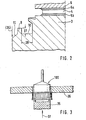
- figure 2 shows a detail from FIG. 1 in a schematic Enlargement
- Figure 3 is a schematic representation of the Procedure for pressing in the rectifier diode
- FIG. 4 a further detail from Figure 1 in a schematic Enlargement
- Figure 5 shows a third detail from Figure 1 in a schematic enlargement.
- FIG. 1 shows a generally designated 100 in one partially cut cross-section shown Rectifier diode.
- the rectifier diode 100 has one Base 2 with a base base 1. With the base 2 is integrally connected to a platform 3, on which in turn, for example by soldering (Lot 5b), a semiconductor chip is appropriate.
- the semiconductor chip 4 is in turn for example again by soldering (Lot 5a) over a Head cylinder 6 and a head cone 7 with a head wire 8 connected.
- the platform 3, which is preferably arranged in the center is of a circumferential wall 9 and one through the wall 9 and the pedestal 3 formed trench 10.
- the head cone 7, the Head cylinder 6, the semiconductor chip 4 and the pedestal 3 are surrounded with a packaging 13 by a protective sleeve 12 is limited.
- the platform 3 and the head cylinder 6 point bevel 16 and / or 17 towards the edge of the semiconductor chip ( Figure 5). These chamfers can, for example, with Lot 18 and / or 19.
- a passivation 14 attached to the chip and the solder on Sealed chip edge.
- the platform 3 also has a encircling shoulder 15 with an inclined edge 20 on the protrudes into the packaging 13.
- the semiconductor chip 4 on a elevated platform 3, which is attached by a wall 9 is surrounded.
- the trench 10 thus formed has typically a length that is approximately twice as long the height of the wall 9.
- the advantage of the invention is in that the construction is particularly robust Deformation when pressing in the rectifier diode.
- the A combination of pedestal and wall / ditch ensures one more homogeneous. and lower bending stress on the Chip contact area compared to a construction without significantly trained wall 9. This robustness is confirmed by finite element calculations.
- Another The advantage is that the chip centering compared to the Construction figure 4 of the font DE 41 12 286 less is critical.
- the construction described there hangs the robustness and reliability of the component is essential from exactly centering the chip during manufacture Fasten.
- the inventive Construction of the wall lower than the pedestal, e.g. to the Access to the chip in the manufacture of the diode and in the Not to affect passivation.
- the rectifier diode 100 has its Socket 2, for example on the circumference of the platform 3, one Shoulder 15 on.
- This optional shoulder serves an intimate form closure of the packaging with the base manufacture.
- the base is hooked to the packaging 13 to a certain extent.
- the shoulder 15 has an oblique edge 20 on, causing the occurrence of high mechanical stresses and the risk of cracks in the packaging on the outside mechanical, but also thermal loads avoided that is at a tapered end of the shoulder would exist.
- FIGs 2 and 3 illustrate the press-in process or the process force acting on the rectifier diode.
- a press-in punch 35 When pressing in the rectifier diode into a rectifier arrangement 36 one uses a press-in punch 35 (see Figure 3), the an insertion force 37 on the base 2 of the rectifier diode 100 transmits.
- the press-in die 35 trained so that it only on an edge region of the Base presses.
- the rectifier arrangement 36 practices one Counterforce 34 on the pressing area 11 of the base of the Rectifier diode 100 off (see Figure 2).
- the Semiconductor chip 4 and the solder layers 5a, 5b surrounding it are significantly higher than the point of attack Force that acts on the base when pressed in and to others are through the circumferential trench 10 from the area strong deformation decoupled.
- the Probability of pressing the chip in damage is significantly reduced. FEM calculations and Tests have also confirmed this.
- the trench designed by a width to depth ratio of 2: 1 so that the base can be manufactured inexpensively. The robust one and simple construction of pedestal with wall and ditch thus allows the use of high press-in forces with minimal Deformation of the semiconductor chip.
- the advantage of the invention here is now the head form from a cylinder and a cone portion.
- the Head cone 7 allows sufficient coverage with Potting compound on the outside diameter, at the same time more compact Construction (small height).
- At an angle 33 of Head cone 7 of typically 20 ° is obtained despite the Cone shape continues to make optimal use of power for the Form locking of packaging and head of approx. 94% of the axial Traction.
- the head is also considerably increased in rigidity and occurring tensile forces evenly on the entire Area distributed.
- the special design of the packaging 13 in the area of Head 6.7 represents a further optimization in the sense a more compact design.
- the packaging 13 is by the Shoulder 15 positively connected to the base 2. Furthermore, the packaging can exert forces on the head. These forces are higher in the edge area of the head than in the Middle of the head in which the head wire is attached.
- the packaging is therefore essential in the edge area of the head designed thicker than in the central area ( Figure 1). So is obtained, for example, from the protective sleeve 12 a slightly increasing course of the packaging 13 to Head wire 8.
- Figure 5 shows a detail of Figure 1 at the edge of the Semiconductor chips 4.
- Point head cylinder 6 and platform 3 a bevel 16 and 17 each on the edge.
- the free area between pedestal and semiconductor chip or semiconductor chip and Head cylinder is for example with lot 18 or 19 refilled.
- the advantage of this is that in the area of maximum diameter for round chips or geometric adapted bases or heads on the entire circumference a thicker layer of solder can be set, whereby the Solder fatigue is drastically reduced.
- the shear of the solder layer is all the more larger, the smaller the layer thickness of the solder and the longer the sheared area.
Landscapes
- Rectifiers (AREA)
- Structures Or Materials For Encapsulating Or Coating Semiconductor Devices Or Solid State Devices (AREA)
- Die Bonding (AREA)
Abstract
Description
Claims (7)
- Gleichrichterdiode mit einem Sockel (2), die in eine vorgesehene Öffnung einer Gleichrichteranordnung (36) einpreßbar ist, wobei auf dem Sockel (2) einstückig mit dem Sockel ein Podest (3) angeordnet ist, auf dem seinerseits ein Halbleiterchip (4) befestigt ist, an dem seinerseits ein Kopfdraht (8) befestigt ist, wobei der Sockel zur thermischen und elektrischen Verbindung der Diode mit der Gleichrichteranordnung dient, und der Sockelboden (1) im Bereich des Podests (3) einen dieses Podest umgebenden Wall (91 auf weist, dass der vom Podest (3) durch einen Graben (10) getrennte Wall (9) mit dem Sockelboden (1) einstückig ist, dass auf der vom Graben (10) abgewandten Seite des Walls (9) zwischen dem Wall und einer zum Sockelboden im Wesentlichen senkrecht angeordneten Wandung des Sockels (2) ein Preßbereich (11) zur Aufnahme von senkrecht zur Ebene des Halbleiterchips (4) gerichteten Kräfte angeordnet ist, dadurch gekennzeichnet, dass der zwischen Wall (9) und Podest (3) ausgebildete Graben (10) eine radiale Ausdehnung hat, die im Wegentlichen doppelt so groß ist wie die Höhe des Walls (9) vom Graben (10) ab gerechnet..
- Gleichrichterdiode nach Anspruch 1, dadurch gekennzeichnet, dass der Kopfdraht (8) über einen Kopfkegel (7) und einen Kopfzylinder (6) mit dem Halbleiterchip (4) verbunden ist.
- Gleichrichterdiode nach Anspruch 2, dadurch gekennzeichnet, dass die Mantellinie des Kopfkegels (7) einen Winkel (33) von etwa 20° zur Ebene des Halbleiterchips (4) und die Gleichrichterdiode eine den Halbleiterchip (4) schützende Verpackung (13) aufweist.
- Gleichrichterdiode nach Anspruch 2 oder 3, dadurch gekennzeichnet, dass sie eine den Halbleiterchip (4) schützende, im Bereich des äußeren Randes des Kopfkegels (7) im Vergleich zum Bereich in der Nähe des Kopfdrahtes (8) dickere Verpackung (13) aufweist.
- Gleichrichterdiode nach einem der vorhergehenden Ansprüche, dadurch gekennzeichnet, dass das Podest (3) und/oder der Kopfzylinder (6) im Bereich des Halbleiterchips (4) am äußeren Rand eine Fase (16 und/oder 17) aufweist und dass im Bereich der Fase (16 und/oder 17) Lot (18 und/oder 19) angebracht ist.
- Gleichrichterdiode nach einem der vorhergehenden Ansprüche, dadurch gekennzeichnet, dass das Podest (3) seitlich eine Schulter (15) aufweist, die in eine den Halbleiterchip (4) schützende Verpackung hineinragt.
- Gleichrichterdiode nach Anspruch 6, dadurch gekennzeichnet, dass die Schulter (15) eine schräge Kante (20) aufweist.
Applications Claiming Priority (3)
| Application Number | Priority Date | Filing Date | Title |
|---|---|---|---|
| DE19549202 | 1995-12-30 | ||
| DE19549202A DE19549202B4 (de) | 1995-12-30 | 1995-12-30 | Gleichrichterdiode |
| PCT/DE1996/002139 WO1997024762A1 (de) | 1995-12-30 | 1996-11-09 | Gleichrichterdiode |
Publications (2)
| Publication Number | Publication Date |
|---|---|
| EP0870328A1 EP0870328A1 (de) | 1998-10-14 |
| EP0870328B1 true EP0870328B1 (de) | 2004-08-18 |
Family
ID=7781679
Family Applications (1)
| Application Number | Title | Priority Date | Filing Date |
|---|---|---|---|
| EP96945714A Expired - Lifetime EP0870328B1 (de) | 1995-12-30 | 1996-11-09 | Gleichrichterdiode |
Country Status (6)
| Country | Link |
|---|---|
| US (1) | US6060776A (de) |
| EP (1) | EP0870328B1 (de) |
| JP (1) | JP4033904B2 (de) |
| KR (1) | KR100471008B1 (de) |
| DE (2) | DE19549202B4 (de) |
| WO (1) | WO1997024762A1 (de) |
Families Citing this family (48)
| Publication number | Priority date | Publication date | Assignee | Title |
|---|---|---|---|---|
| DE19739083C2 (de) * | 1997-09-06 | 2001-09-27 | Bosch Gmbh Robert | Gehäuse mit einem planaren Leistungstransistor |
| DE10005183A1 (de) | 2000-02-05 | 2001-08-09 | Bosch Gmbh Robert | Gleichrichteranordnung |
| KR100361695B1 (ko) * | 2000-04-03 | 2002-11-22 | 주식회사 케이이씨 | 정류 다이오드 제조방법 |
| RU2201016C2 (ru) * | 2000-12-14 | 2003-03-20 | Новиков Александр Васильевич | Конструкция силового полупроводникового прибора |
| DE10100882A1 (de) * | 2001-01-11 | 2002-08-01 | Bosch Gmbh Robert | Verfahren zur Montage eines Halbleiterbauelementes und Halbleiterbauelement |
| US6559529B2 (en) * | 2001-04-10 | 2003-05-06 | International Rectifier Corporation | Press-fit diode for universal mounting |
| RU2229756C2 (ru) * | 2001-12-11 | 2004-05-27 | Барашков Александр Алексеевич | Конструкция полупроводникового прибора |
| DE10160872B3 (de) * | 2001-12-12 | 2005-05-19 | Robert Bosch Gmbh | Vorrichtung mit einem Leistungshalbleiterbauelement |
| TW560701U (en) * | 2002-01-21 | 2003-11-01 | Yenyo Technology Co Ltd | Improved press-fit package diode |
| DE10323492A1 (de) | 2002-05-24 | 2003-12-04 | Bosch Gmbh Robert | Elektrisches Bauelement |
| US7677579B2 (en) * | 2002-05-31 | 2010-03-16 | Technip France Sa | Seal assembly for dividing an annular space in a double-walled pipeline |
| DE10242521A1 (de) * | 2002-09-12 | 2004-03-25 | Robert Bosch Gmbh | Diode |
| US7091582B2 (en) * | 2002-11-27 | 2006-08-15 | Mario Merlin | Electronic package with snap-on perimeter wall |
| RU2231863C1 (ru) * | 2002-11-27 | 2004-06-27 | Новиков Александр Васильевич | Конструкция полупроводникового прибора |
| EP1443546A3 (de) * | 2003-01-28 | 2009-05-06 | Hitachi Ltd. | Verfahren zur Metallbearbeitung und mit diesem Verfahren hergestelltes Halbleiterbauelement |
| US6894377B2 (en) * | 2003-06-23 | 2005-05-17 | Wen-Huo Huang | Rectification chip terminal structure |
| DE10346855A1 (de) * | 2003-08-18 | 2005-03-17 | Robert Bosch Gmbh | Einpressdiode mit versilbertem Drahtanschluss |
| EP1658637A1 (de) * | 2003-08-18 | 2006-05-24 | Robert Bosch Gmbh | Einpressdiode mit versilbertem drahtanschluss |
| US7239016B2 (en) * | 2003-10-09 | 2007-07-03 | Denso Corporation | Semiconductor device having heat radiation plate and bonding member |
| TW200527618A (en) * | 2003-11-10 | 2005-08-16 | Bosch Gmbh Robert | Diode |
| US6958530B1 (en) * | 2004-08-31 | 2005-10-25 | Sung Jung Minute Industry Co., Ltd. | Rectification chip terminal structure |
| US7009223B1 (en) * | 2004-08-31 | 2006-03-07 | Sung Jung Minute Industry Co., Ltd. | Rectification chip terminal structure |
| US8159072B2 (en) | 2007-12-12 | 2012-04-17 | Wen-Huo Huang | Rectification chip terminal structure |
| US20090152711A1 (en) * | 2007-12-12 | 2009-06-18 | Wen-Huo Huang | Rectification chip terminal structure |
| DE102007060371B4 (de) | 2007-12-12 | 2016-12-15 | Sung Jung Minute Industry Co., Ltd. | Gleichrichterchip- Anschluss- Struktur |
| DE102007060231A1 (de) * | 2007-12-14 | 2009-06-18 | Robert Bosch Gmbh | Generator mit Gleichrichteranordnung |
| DE102007063308A1 (de) | 2007-12-28 | 2009-07-02 | Robert Bosch Gmbh | Diode |
| TW200941734A (en) * | 2008-03-20 | 2009-10-01 | Sung Jung Minute Industry Co Ltd | A packaging structure of a rectifier diode |
| JP5341380B2 (ja) * | 2008-04-04 | 2013-11-13 | 株式会社日立製作所 | 半導体装置 |
| DE102009002100A1 (de) | 2009-04-01 | 2010-10-07 | Robert Bosch Gmbh | Elektrisches Bauelement |
| US20100303610A1 (en) * | 2009-05-29 | 2010-12-02 | United Technologies Corporation | Cooled gas turbine stator assembly |
| DE102010028199A1 (de) | 2010-04-26 | 2011-10-27 | Robert Bosch Gmbh | Einpressdiode |
| DE102010028207A1 (de) | 2010-04-26 | 2011-10-27 | Robert Bosch Gmbh | Gleichrichter-Brückenschaltung |
| DE102010038879A1 (de) * | 2010-08-04 | 2012-02-09 | Robert Bosch Gmbh | Gleichrichteranordnung, welche Einpressdioden aufweist |
| DE102010062677A1 (de) | 2010-12-09 | 2012-06-14 | Robert Bosch Gmbh | Generatorvorrichtung zur Spannungsversorgung eines Kraftfahrzeugs |
| DE102010063041A1 (de) | 2010-12-14 | 2012-06-14 | Robert Bosch Gmbh | Generatorvorrichtung mit verbesserter Verpolfestigkeit |
| JP2012174878A (ja) * | 2011-02-22 | 2012-09-10 | Hitachi Ltd | 半導体装置、及びそれを用いた装置 |
| DE102012207654A1 (de) | 2012-05-08 | 2013-11-14 | Robert Bosch Gmbh | Kraftfahrzeug-Generatorvorrichtung mit einer Schutzanordnung zur Störsignalunterdrückung |
| US9324625B2 (en) | 2012-05-31 | 2016-04-26 | Infineon Technologies Ag | Gated diode, battery charging assembly and generator assembly |
| US8847366B1 (en) * | 2013-03-12 | 2014-09-30 | Jung-Chi HSIEN | Rectifier diode |
| DE102013204701A1 (de) | 2013-03-18 | 2014-10-02 | Robert Bosch Gmbh | Pseudo-Schottky-Diode |
| US10035703B2 (en) * | 2013-09-27 | 2018-07-31 | Continental Automotive Systems, Inc. | Die bond design for medium pressure sensor |
| DE102013220011B4 (de) | 2013-10-02 | 2025-01-02 | Robert Bosch Gmbh | Halbleiteranordnung mit temperaturkompensierter Durchbruchsspannung |
| DE102014209117B4 (de) * | 2014-05-14 | 2020-01-23 | Robert Bosch Gmbh | Diode |
| DE102014212455B4 (de) | 2014-06-27 | 2024-07-04 | Robert Bosch Gmbh | Diode mit einem plattenförmigen Halbleiterelement |
| JP7231407B2 (ja) * | 2018-12-27 | 2023-03-01 | 株式会社 日立パワーデバイス | 半導体装置およびそれを用いたオルタネータ |
| CN111916401A (zh) * | 2020-08-28 | 2020-11-10 | 江苏英达富电子科技有限公司 | 一种车用整流二极管基座及车用整流二极管 |
| US12184161B2 (en) | 2021-10-01 | 2024-12-31 | Advanced Energy Industries, Inc. | Reduced ripple in switch mode power supply with snubber |
Family Cites Families (11)
| Publication number | Priority date | Publication date | Assignee | Title |
|---|---|---|---|---|
| DE2027598A1 (de) * | 1970-06-04 | 1971-12-09 | Siemens Ag | Halbleiterbauelement mit Kunststoff abdeckung |
| US3823339A (en) * | 1972-10-04 | 1974-07-09 | Electronic Labor International | Diode rectifier socketed electrical devices and diode rectifiers therefor |
| DE2755404A1 (de) * | 1977-12-13 | 1979-06-21 | Bosch Gmbh Robert | Halbleiteranordnung |
| US4303935A (en) * | 1977-12-13 | 1981-12-01 | Robert Bosch Gmbh | Semiconductor apparatus with electrically insulated heat sink |
| FR2453500A1 (fr) * | 1979-04-04 | 1980-10-31 | Sev Alternateurs | Dispositif redresseur pour alternateur de vehicule automobile |
| DE8003735U1 (de) * | 1980-02-13 | 1981-07-23 | Robert Bosch Gmbh, 7000 Stuttgart | Halbleiterbauelement |
| FR2512275A3 (fr) * | 1981-08-29 | 1983-03-04 | Bosch Gmbh Robert | Dispositif redresseur de courant avec plaquette a diode a semi-conducteur |
| US4896062A (en) * | 1988-06-03 | 1990-01-23 | Westinghouse Electric Corp. | Rotating rectifier assembly |
| US5005069A (en) * | 1990-04-30 | 1991-04-02 | Motorola Inc. | Rectifier and method |
| DE4341269A1 (de) * | 1993-12-03 | 1995-06-22 | Bosch Gmbh Robert | Gleichrichterdiode |
| JP3550243B2 (ja) * | 1996-01-30 | 2004-08-04 | 株式会社東芝 | 内部圧接型半導体装置 |
-
1995
- 1995-12-30 DE DE19549202A patent/DE19549202B4/de not_active Expired - Fee Related
-
1996
- 1996-11-09 KR KR10-1998-0704549A patent/KR100471008B1/ko not_active Expired - Lifetime
- 1996-11-09 WO PCT/DE1996/002139 patent/WO1997024762A1/de not_active Ceased
- 1996-11-09 EP EP96945714A patent/EP0870328B1/de not_active Expired - Lifetime
- 1996-11-09 JP JP52396197A patent/JP4033904B2/ja not_active Expired - Lifetime
- 1996-11-09 DE DE59611062T patent/DE59611062D1/de not_active Expired - Lifetime
- 1996-11-09 US US09/091,973 patent/US6060776A/en not_active Expired - Lifetime
Also Published As
| Publication number | Publication date |
|---|---|
| US6060776A (en) | 2000-05-09 |
| KR100471008B1 (ko) | 2005-07-07 |
| JP2000502838A (ja) | 2000-03-07 |
| DE19549202B4 (de) | 2006-05-04 |
| DE59611062D1 (de) | 2004-09-23 |
| KR19990072188A (ko) | 1999-09-27 |
| DE19549202A1 (de) | 1997-07-03 |
| JP4033904B2 (ja) | 2008-01-16 |
| EP0870328A1 (de) | 1998-10-14 |
| WO1997024762A1 (de) | 1997-07-10 |
Similar Documents
| Publication | Publication Date | Title |
|---|---|---|
| DE19549202B4 (de) | Gleichrichterdiode | |
| EP0731984B1 (de) | Gleichrichterdiode | |
| DE4112286A1 (de) | Verbesserter gleichrichter und verfahren zu seiner herstellung | |
| DE2733724C2 (de) | Verfahren zur Herstellung eines Halbleiterbauelements | |
| DE10101078A1 (de) | Halbleitervorrichtung für den Anschluß elektrischer Leistung | |
| DE2617269A1 (de) | Blindniet | |
| EP1960731A1 (de) | Pyrotechnische aktuatoreinheit, verfahren zu deren herstellung sowie gassackmodul mit einer solchen aktuatoreinheit | |
| DE2651088A1 (de) | Zwischenlegscheibeneinheit zur spannungsanzeige | |
| EP1685594B1 (de) | Einpressdiode | |
| EP3528370A1 (de) | Stator mit einer wicklungsverschaltung | |
| DE19536982A1 (de) | Verfahren und Vorrichtung zur Übertragung von Kräften zwischen zwei Fügeteilen | |
| DE2836976A1 (de) | Buerstenanordnung fuer elektromotoren sowie verfahren zur montage einer buerstenanordnung | |
| DE202012010193U1 (de) | Carbonfaser-Bauteil mit elektrischem Kontaktelement | |
| WO1995022185A1 (de) | Armierungsring für rotationskörper und verfahren zu seiner herstellung | |
| DE2426113A1 (de) | Thyristor-halbleiteranordnung | |
| EP1540726A1 (de) | Diode | |
| DE19933891A1 (de) | Blindniet | |
| EP1563519B1 (de) | Elektrische kontaktierung dünner lackdrähte von sekundärwicklungen von zündspulen | |
| EP0139882B1 (de) | Verbindung zwischen Ankerwicklungsenden und zugeordneten Segmenten eines Kommutators | |
| EP1001493A2 (de) | Baugruppe aus einem Halteteil und einem darin eingegossenen Kontaktstift | |
| DE10310067B4 (de) | Halbleitervorrichtung mit hohlzylindrischer Gehäuseelektrode | |
| DE20017234U1 (de) | Käfigmutter sowie Werkzeug zum Fixieren der Käfigmutter | |
| DE19924212A1 (de) | Verfahren zum Bonden von Leitern, insbesondere Beam Leads | |
| DE102006019315B4 (de) | Gleichrichter für eine Elektromaschine | |
| DE102023211921A1 (de) | Vorrichtung zur Anordnung einer Dichtung, Stator und Fahrzeug |
Legal Events
| Date | Code | Title | Description |
|---|---|---|---|
| PUAI | Public reference made under article 153(3) epc to a published international application that has entered the european phase |
Free format text: ORIGINAL CODE: 0009012 |
|
| 17P | Request for examination filed |
Effective date: 19980730 |
|
| AK | Designated contracting states |
Kind code of ref document: A1 Designated state(s): DE FR GB IT |
|
| 17Q | First examination report despatched |
Effective date: 20000925 |
|
| APAB | Appeal dossier modified |
Free format text: ORIGINAL CODE: EPIDOS NOAPE |
|
| APAB | Appeal dossier modified |
Free format text: ORIGINAL CODE: EPIDOS NOAPE |
|
| APAD | Appeal reference recorded |
Free format text: ORIGINAL CODE: EPIDOS REFNE |
|
| APBT | Appeal procedure closed |
Free format text: ORIGINAL CODE: EPIDOSNNOA9E |
|
| GRAP | Despatch of communication of intention to grant a patent |
Free format text: ORIGINAL CODE: EPIDOSNIGR1 |
|
| GRAS | Grant fee paid |
Free format text: ORIGINAL CODE: EPIDOSNIGR3 |
|
| GRAA | (expected) grant |
Free format text: ORIGINAL CODE: 0009210 |
|
| AK | Designated contracting states |
Kind code of ref document: B1 Designated state(s): DE FR GB IT |
|
| REG | Reference to a national code |
Ref country code: GB Ref legal event code: FG4D Free format text: NOT ENGLISH |
|
| REF | Corresponds to: |
Ref document number: 59611062 Country of ref document: DE Date of ref document: 20040923 Kind code of ref document: P |
|
| GBT | Gb: translation of ep patent filed (gb section 77(6)(a)/1977) |
Effective date: 20041215 |
|
| ET | Fr: translation filed | ||
| PLBE | No opposition filed within time limit |
Free format text: ORIGINAL CODE: 0009261 |
|
| STAA | Information on the status of an ep patent application or granted ep patent |
Free format text: STATUS: NO OPPOSITION FILED WITHIN TIME LIMIT |
|
| 26N | No opposition filed |
Effective date: 20050519 |
|
| APAH | Appeal reference modified |
Free format text: ORIGINAL CODE: EPIDOSCREFNO |
|
| PGFP | Annual fee paid to national office [announced via postgrant information from national office to epo] |
Ref country code: GB Payment date: 20131122 Year of fee payment: 18 Ref country code: FR Payment date: 20131119 Year of fee payment: 18 |
|
| PGFP | Annual fee paid to national office [announced via postgrant information from national office to epo] |
Ref country code: IT Payment date: 20131126 Year of fee payment: 18 |
|
| REG | Reference to a national code |
Ref country code: DE Ref legal event code: R084 Ref document number: 59611062 Country of ref document: DE Effective date: 20140417 |
|
| GBPC | Gb: european patent ceased through non-payment of renewal fee |
Effective date: 20141109 |
|
| REG | Reference to a national code |
Ref country code: FR Ref legal event code: ST Effective date: 20150731 |
|
| PG25 | Lapsed in a contracting state [announced via postgrant information from national office to epo] |
Ref country code: GB Free format text: LAPSE BECAUSE OF NON-PAYMENT OF DUE FEES Effective date: 20141109 |
|
| PG25 | Lapsed in a contracting state [announced via postgrant information from national office to epo] |
Ref country code: FR Free format text: LAPSE BECAUSE OF NON-PAYMENT OF DUE FEES Effective date: 20141201 |
|
| PG25 | Lapsed in a contracting state [announced via postgrant information from national office to epo] |
Ref country code: IT Free format text: LAPSE BECAUSE OF NON-PAYMENT OF DUE FEES Effective date: 20141109 |
|
| PGFP | Annual fee paid to national office [announced via postgrant information from national office to epo] |
Ref country code: DE Payment date: 20160126 Year of fee payment: 20 |
|
| REG | Reference to a national code |
Ref country code: DE Ref legal event code: R071 Ref document number: 59611062 Country of ref document: DE |