EP0868741B1 - Shape memory alloy lift pins for a semiconductor processing equipment - Google Patents
Shape memory alloy lift pins for a semiconductor processing equipment Download PDFInfo
- Publication number
- EP0868741B1 EP0868741B1 EP96944410A EP96944410A EP0868741B1 EP 0868741 B1 EP0868741 B1 EP 0868741B1 EP 96944410 A EP96944410 A EP 96944410A EP 96944410 A EP96944410 A EP 96944410A EP 0868741 B1 EP0868741 B1 EP 0868741B1
- Authority
- EP
- European Patent Office
- Prior art keywords
- substrate
- lift
- lift pin
- lifter
- lift pins
- Prior art date
- Legal status (The legal status is an assumption and is not a legal conclusion. Google has not performed a legal analysis and makes no representation as to the accuracy of the status listed.)
- Expired - Lifetime
Links
Images
Classifications
-
- H—ELECTRICITY
- H10—SEMICONDUCTOR DEVICES; ELECTRIC SOLID-STATE DEVICES NOT OTHERWISE PROVIDED FOR
- H10P—GENERIC PROCESSES OR APPARATUS FOR THE MANUFACTURE OR TREATMENT OF DEVICES COVERED BY CLASS H10
- H10P95/00—Generic processes or apparatus for manufacture or treatments not covered by the other groups of this subclass
-
- H—ELECTRICITY
- H10—SEMICONDUCTOR DEVICES; ELECTRIC SOLID-STATE DEVICES NOT OTHERWISE PROVIDED FOR
- H10P—GENERIC PROCESSES OR APPARATUS FOR THE MANUFACTURE OR TREATMENT OF DEVICES COVERED BY CLASS H10
- H10P72/00—Handling or holding of wafers, substrates or devices during manufacture or treatment thereof
- H10P72/70—Handling or holding of wafers, substrates or devices during manufacture or treatment thereof for supporting or gripping
- H10P72/76—Handling or holding of wafers, substrates or devices during manufacture or treatment thereof for supporting or gripping using mechanical means, e.g. clamps or pinches
- H10P72/7604—Handling or holding of wafers, substrates or devices during manufacture or treatment thereof for supporting or gripping using mechanical means, e.g. clamps or pinches the wafers being placed on a susceptor, stage or support
- H10P72/7612—Handling or holding of wafers, substrates or devices during manufacture or treatment thereof for supporting or gripping using mechanical means, e.g. clamps or pinches the wafers being placed on a susceptor, stage or support characterised by lifting arrangements, e.g. lift pins
-
- G—PHYSICS
- G03—PHOTOGRAPHY; CINEMATOGRAPHY; ANALOGOUS TECHNIQUES USING WAVES OTHER THAN OPTICAL WAVES; ELECTROGRAPHY; HOLOGRAPHY
- G03F—PHOTOMECHANICAL PRODUCTION OF TEXTURED OR PATTERNED SURFACES, e.g. FOR PRINTING, FOR PROCESSING OF SEMICONDUCTOR DEVICES; MATERIALS THEREFOR; ORIGINALS THEREFOR; APPARATUS SPECIALLY ADAPTED THEREFOR
- G03F7/00—Photomechanical, e.g. photolithographic, production of textured or patterned surfaces, e.g. printing surfaces; Materials therefor, e.g. comprising photoresists; Apparatus specially adapted therefor
- G03F7/70—Microphotolithographic exposure; Apparatus therefor
- G03F7/70691—Handling of masks or workpieces
- G03F7/707—Chucks, e.g. chucking or un-chucking operations or structural details
- G03F7/70708—Chucks, e.g. chucking or un-chucking operations or structural details being electrostatic; Electrostatically deformable vacuum chucks
-
- Y—GENERAL TAGGING OF NEW TECHNOLOGICAL DEVELOPMENTS; GENERAL TAGGING OF CROSS-SECTIONAL TECHNOLOGIES SPANNING OVER SEVERAL SECTIONS OF THE IPC; TECHNICAL SUBJECTS COVERED BY FORMER USPC CROSS-REFERENCE ART COLLECTIONS [XRACs] AND DIGESTS
- Y10—TECHNICAL SUBJECTS COVERED BY FORMER USPC
- Y10S—TECHNICAL SUBJECTS COVERED BY FORMER USPC CROSS-REFERENCE ART COLLECTIONS [XRACs] AND DIGESTS
- Y10S156/00—Adhesive bonding and miscellaneous chemical manufacture
- Y10S156/914—Differential etching apparatus including particular materials of construction
Definitions
- the invention relates to a lift pin arrangement for lifting substrates such as semiconductor wafers or flat panel display substrates.
- lift pin mechanisms can be used in temporarily supporting the substrates during transfer, thermal, chemical, optical and other treatments of the substrates.
- Plasma generation is used in a variety of such semiconductor fabrication processes.
- Plasma generating equipment includes parallel plate reactors such as the type disclosed in commonly owned U.S. Patent No. 4,340,462, electron cyclotron resonance (ECR) systems such as the type disclosed in commonly owned U.S. Patent No. 5,200,232 and inductively coupled plasma systems such as the type disclosed in commonly owned U.S. Patent No. 4.948,458,
- ECR electron cyclotron resonance
- it is conventional to support the substrate to be treated on a substrate holder within a portion of a plasma process chamber. Further, it is conventional to hold the substrate on the substrate holder by mechanical and/or electrostatic clamping mechanisms.
- An example of a mechanical clamping system is disclosed in U.S. Patent No. 4,615,755 and an example of an electrostatic chucking (ESC) arrangement is disclosed in U.S. Patent No. 4,554,611.
- ESC electrostatic chucking
- a substrate such as a wafer into a substrate processing chamber
- robot arm and lift pin arrangements such as the types disclosed in U.S. Patent Nos. 4,431,473, 4,790,258, 4,842,683 and 5,215,619.
- a lift pin arrangement such as the type disclosed in the U.S Patent No. 4,431,473 wherein four lift pins are arranged in a circular pattern which is concentric with a substrate in the form of a wafer.
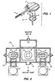
- a wafer 2 is supported on a robotic arm 4 and a lift pin mechanism 8 having four lift pins 6 is below the wafer 2.
- the lift pin mechanism can be utilized in a semiconductor processing apparatus 10 having an entrance load 12, a substrate processing chamber 14 and an exit load lock 16.
- lift pin arrangements are very delicate and the lift pins are extremely easy to bend under a variety of circumstances. For instance, the lift pins can be bent during substrate holder maintenance, substrate handling adjustments, malfunctions of the handler/ESC/clamp, and manual operation of the substrate transport system. Once bent the lift pins must be removed in order to be repaired. Usually the lift pins assembly must be completely replaced since any repair would require a very delicate, precise operation. Further, problems relating to bending of the lift pins contribute to (1) reduced system up time, (2) longer mean time to repair (MTTR), (3) increased maintenance/part costs and (4) possibly . increased particle levels in the processor.
- MTTR mean time to repair
- JP60167346A and Patents Abstracts of Japan Vol 10 No 1 (E [371]) describes a device which raises and lowers a substrate by heating and cooling of a heat elastic material which expands or contracts.
- a lift pin mechanism in accordance with claim 1.
- the shape memory alloy is preferably transformable from a martensitic state to an austenitic state and the lift pin is restorable from a deformed configuration to the memorized configuration by heating the lift pin to a temperature at which the shape memory alloy transforms to the austenitic state.
- the shape memory alloy can have a martensite- to- austenite transformation temperature such as above or below ambient temperature.
- the lift pin is preferably supported on a lifter forming part of a substrate holder of a substrate processing apparatus wherein the lifter is movable in a vertical direction between upper and lower positions.
- the lifter can be movable such that the lift pin has an upper surface located above a substrate support surface of the substrate holder when the lifter is in the upper position and the upper surface of the lift pin is below the substrate support surface when the lift pin is in the lower position.
- part of the lift pin passes through a lift pin hole in the substrate holder when the lifter moves from the lower position to the upper position.
- the lift pin hole functions to supply heat transfer gas to an underside of the substrate, to allow adequate flow of gas the lift pin can have cross section which fills 55 to 75% of the lift pin hole.
- the lift pin can be a rectilinearly extending cylindrical pin press fitted in the lifter and the lifter can be of various materials such as plastic. ceramic, or metal or combinations thereof.
- the invention also provides a process according to claim 8.
- the process includes (1) moving a robotic arm supporting to a substrate to be processed such that the substrate is transferred to a process position in a substrate processing chamber, (2) raising a lifter having a plurality of lift pins to an upper position at which the substrate is supported on the upper ends of the lift pins, each of the lift pins consisting essentially of a shape memory alloy having a memorized configuration, (3) retracting the robot arm away from the substrate, (4) lowering the lifter to a lower position at which the substrate is supported on a substrate holder in the substrate processing chamber, (5) clamping the substrate to the substrate holder, (6) processing the substrate, (7) unclamping the substrate, (8) raising the lifter to an upper position and (9) transferring the substrate out of the substrate processing chamber.
- the substrate is supported on the lift pins during transfer of the substrate from one process position to another process position of a substrate processing apparatus.
- the process includes (1) moving a first robotic arm supporting a substrate to be transferred such that the substrate is transferred from a first process position to a staging position, (2) raising a lifter having a plurality of lift pins to an upper position at which the substrate is supported on upper ends of the lift pins, each of the lift pins consisting essentially of a shape memory alloy having a memorized configuration, (3) retracting the first robotic arm away from the substrate, (4) moving a second robotic arm into a position to receive the substrate, (5) lowering the lifter to a lower position so that the substrate is supported by the second robotic arm, and (6) transferring the substrate from the staging position to a second process position.
- the transferring or processing can be carried out utilizing for the lift pins a shape memory alloy which is transformable at a temperature above or below ambient from a martensitic state to an austenitic state wherein and the lift pin is restorable from a deformed configuration to the memorized configuration by applying heat to the lift pin or operating the equipment at a temperature which exposes the lift pin to a temperature at which the shape memory alloy transforms to the austenitic state.
- the process can include restoring at least one of the lift pins from the deformed configuration to the memorized condition by heating the lift pin to a temperature at which the shape memory alloy transforms from martensitic state to the austenitic state.
- each of the lift pins can pass through a lift pin hole in a water cooled substrate holder when the lifter moves from the lower position to the upper position and each of the lift pins can have a cross section which fills 55 to 75% of the lift pin hole.
- the space between the pins and the holes allows pressurized cooling gas to be supplied between the substrate and the substrate holder to allow temperature control of the substrate.
- the invention provides a lift pin mechanism for substrate handling equipment wherein the lift pins have extremely high elasticity and possibly heat recoverability which allows damaged lift pins to be restraightened without removal from the lift pin arrangement.
- the lift pins are of a superelastic and/or shape memory alloy based on the nickel-titanium system (e.g., Nitinol, a NiTi alloy having 53-57 wt % Ni with or without additional alloying elements).
- Nitinol a NiTi alloy having 53-57 wt % Ni with or without additional alloying elements.
- Such materials exhibit the "superelastic effect" where, if subjected to a mechanical strain sufficient to cause substantial bending (e.g., over 3% strain), the material returns immediately to its original shape as soon as the force causing the strain is removed.
- thin wires of a superelastic alloy can be used to provide a lift pin arrangement which will accommodate dramatic bends of the lift pins without permanent distortion thereof. Further, if the lift pins become deformed, the heat recoverable property of the alloy can be used to recover the original shape of the lift pins.
- the superelastic effect is known to occur through the formation of stress-induced martensite. That is, when a shape memory alloy exhibiting stress-induced martensite is stressed at a temperature above M S (so that the austenitic state is initially stable), but below M d (the maximum temperature at which martensite formation can occur even under stress) it first deforms elastically and then at a critical stress, begins to transform elastically by the formation of stress-induced martensite. Upon release of the stress, the stress-induced martensite transforms back to austenite and the material returns to its original configuration. Thus, the material can recover elastically from strains of more than 3% and possibly as much as 6 or 8% whereas most conventional materials are permanently deformed when subjected to as little as 1% strain.
- the temperature at which the shape memory alloy transforms from the martensitic to the austenitic state can be adjusted by appropriate thermomechanical treatment and/or alloying of the shape memory alloy.
- U.S. Patent No. 4,894,100 discloses a Ni-Ti-V alloy wherein the M S temperature can be adjusted by varying the Ni/Ti ratio and V content.
- the '100 patent discloses that an M S of 20-70°C can be provided by adjusting the ratio of Ni/Ti to 0.96-1.02 whereas an M S of -150 to 20°C can be provided by adjusting the ratio of Ni/Ti to 1.0-1.06.
- an M S of -10 to 20°C can be provided.
- various alloys and thermomechanical treatments thereof can be utilized to provide the lifting pins in accordance with the invention.
- the lift pins can be of a shape memory material such as Nitinol which is formed into a memorized configuration by appropriate thermomechanical treatment.
- the lift pins can be rectilinearly extending cylindrical Nitinol pins which have an M s no greater than 25°C, e.g., 5°C.
- the lift pins can have an M s of greater than 25°C.
- the lift pins are operated in an environment in which the lift pins are normally in the austenitic condition. Thus, the lift pins will exhibit the superelastic effect as a result of the ability to form stress-induced martensite.
- the lift pins can also be used in an environment in which the lift pins are in the martensitic condition. In either case, if the lift pins are deformed in the martensitic state beyond the elastic limit, the lift pins can be restored to their memorized configuration simply by heating the lift pins into the austenitic state.
- the lift pin arrangement can be used in various parts of substrate processing apparatus such as in load locks and/or substrate processing chambers.
- the substrate can be transferred by robotic arm or other suitable mechanism to a position at which lift pins lift the substrate off of a support surface of the robotic arm, the robotic arm is withdrawn and the substrate is lowered onto a support surface of the same or another robotic arm, a substrate holder, or the like.
- the substrate processing chamber can be used to perform various treatments such as etching, deposition, resist stripping, photolithography, CVD, RTP, ion implantation or sputtering, or the like, on the substrate supported on the substrate holder.
- etching layers such as polysilicon, oxide or a metal such as aluminum or tungsten can be carried out in a substrate processing chamber.
- oxide etching the temperature within the substrate processing chamber can be maintained below 0°C such as at about -20°C.
- the lift pins will be in the martensitic state during the etching process and if the lift pins become bent as a result of movement and/or supporting the wafer during transfer thereof into or out of the substrate processing chamber or into or out of contact with the substrate holder, the lift pins can be restored to their original memorized straight condition simply by allowing the substrate processing chamber to heat the lift pins to room temperature.
- the lift pins will transform from the martensitic to the austenitic state and the lift pins will automatically straighten as a result of the martensitic-to-austenitic phase change.
- the heating to heat recover the memorized shape can also be achieved by other techniques such as by applying a sufficient electrical current through the lift pins or by heating the lift pins with a heat gun.
- the substrate can be supported on the substrate holder by any suitable restraining apparatus.
- the substrate holder can incorporate an electrostatic chucking or ESC arrangement for clamping the substrate to the substrate holder.
- a mechanical clamping arrangement can be provided for holding the substrate to the substrate holder.
- a clamping ring can be used to clamp the wafer to the substrate holder.
- the lift pins remain at least partially in the holes in the substrate holder when the lifter assembly is in the bottom position and the clearance between the lift pins and the holes is maintained such that sufficient helium flows to the backside of the substrate.
- the lift pins are of Nitinol having an M S of 5°C.
- the lift pins 20 comprise thin wires press fitted in four holes of a lifter 22.
- the lifter 22 includes a central hole 24 through which a screw passes for attaching the lifter 22 to a pneumatic or mechanical actuator 26.
- the lifter 22 has a thickness of about 5 mm (0.2 inch) and a diameter of about 4.1 mm (1.6 inch) and the lift pins 20 are located about 2.5 mm (0.1 inch) inside of the outer periphery of the lifter 22.
- the lifter also includes an alignment hole 28 for purposes of aligning the lifter 22 with a corresponding hole 30 in the actuator 26 when the lifter 22 is assembled in a plasma treating apparatus.
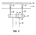
- the lift pins have a length of about 25 mm (1 inch) and a diameter of about 0.75 mm (0.03 inch.)
- the lift pins pass through corresponding holes 32 in a substrate holder 34 in a substrate processing chamber and such holes in the substrate holder have a diameter of about 1 mm (0.04 inch.)
- sufficient clearance is provided between the periphery of the lift pins and the inner periphery of the holes 32 in the substrate holder to allow passage of a suitable cooling gas such as helium into contact with the reverse side of a substrate 36 treated in the substrate processing chamber.
- the ratio of the cross section of the lifting pin versus the cross section of the corresponding hole in the substrate holder can range from 55 to 75%, preferably being about 60%.
- any amount of clearance can be provided between the lift pins and the lift pin holes.
Landscapes
- Physics & Mathematics (AREA)
- General Physics & Mathematics (AREA)
- Container, Conveyance, Adherence, Positioning, Of Wafer (AREA)
- Crystals, And After-Treatments Of Crystals (AREA)
Applications Claiming Priority (3)
| Application Number | Priority Date | Filing Date | Title |
|---|---|---|---|
| US577520 | 1995-12-22 | ||
| US08/577,520 US5669977A (en) | 1995-12-22 | 1995-12-22 | Shape memory alloy lift pins for semiconductor processing equipment |
| PCT/US1996/020028 WO1997023899A1 (en) | 1995-12-22 | 1996-12-18 | Shape memory alloy lift pins for semiconductor processing equipment |
Publications (2)
| Publication Number | Publication Date |
|---|---|
| EP0868741A1 EP0868741A1 (en) | 1998-10-07 |
| EP0868741B1 true EP0868741B1 (en) | 2003-10-08 |
Family
ID=24309090
Family Applications (1)
| Application Number | Title | Priority Date | Filing Date |
|---|---|---|---|
| EP96944410A Expired - Lifetime EP0868741B1 (en) | 1995-12-22 | 1996-12-18 | Shape memory alloy lift pins for a semiconductor processing equipment |
Country Status (8)
| Country | Link |
|---|---|
| US (1) | US5669977A (enExample) |
| EP (1) | EP0868741B1 (enExample) |
| JP (1) | JP2000502508A (enExample) |
| KR (1) | KR100461996B1 (enExample) |
| CN (1) | CN1209216A (enExample) |
| AT (1) | ATE251800T1 (enExample) |
| DE (1) | DE69630314T2 (enExample) |
| WO (1) | WO1997023899A1 (enExample) |
Families Citing this family (44)
| Publication number | Priority date | Publication date | Assignee | Title |
|---|---|---|---|---|
| JP3028462B2 (ja) * | 1995-05-12 | 2000-04-04 | 東京エレクトロン株式会社 | 熱処理装置 |
| US5885353A (en) | 1996-06-21 | 1999-03-23 | Micron Technology, Inc. | Thermal conditioning apparatus |
| US5848670A (en) * | 1996-12-04 | 1998-12-15 | Applied Materials, Inc. | Lift pin guidance apparatus |
| US6168668B1 (en) * | 1998-11-25 | 2001-01-02 | Applied Materials, Inc. | Shadow ring and guide for supporting the shadow ring in a chamber |
| JP2000223549A (ja) * | 1999-01-29 | 2000-08-11 | Canon Inc | 基板搬送装置、基板搬送方法、基板搬送用ハンド機構、灰化処理装置及び灰化処理方法 |
| US6236300B1 (en) | 1999-03-26 | 2001-05-22 | R. Sjhon Minners | Bistable micro-switch and method of manufacturing the same |
| US6572708B2 (en) * | 2000-02-28 | 2003-06-03 | Applied Materials Inc. | Semiconductor wafer support lift-pin assembly |
| US6958098B2 (en) * | 2000-02-28 | 2005-10-25 | Applied Materials, Inc. | Semiconductor wafer support lift-pin assembly |
| US6640432B1 (en) * | 2000-04-12 | 2003-11-04 | Formfactor, Inc. | Method of fabricating shaped springs |
| US7324635B2 (en) | 2000-05-04 | 2008-01-29 | Telemaze Llc | Branch calling and caller ID based call routing telephone features |
| US6422010B1 (en) * | 2000-06-11 | 2002-07-23 | Nitinol Technologies, Inc. | Manufacturing of Nitinol parts and forms |
| KR100769826B1 (ko) * | 2001-05-22 | 2007-10-23 | 엘지.필립스 엘시디 주식회사 | 리프터핀 유닛 |
| TW588403B (en) * | 2001-06-25 | 2004-05-21 | Tokyo Electron Ltd | Substrate treating device and substrate treating method |
| DE10134513A1 (de) * | 2001-07-16 | 2003-01-30 | Unaxis Balzers Ag | Hebe-und Stützvorichtung |
| DE10232478A1 (de) * | 2002-07-17 | 2004-02-12 | Infineon Technologies Ag | Waferhubvorrichtung |
| US6779963B2 (en) * | 2002-11-21 | 2004-08-24 | General Electric Company | Apparatus and method to control force exerted on steam turbines by inlet pipes |
| EP1475667A1 (en) * | 2003-05-09 | 2004-11-10 | ASML Netherlands B.V. | Lithographic apparatus and device manufacturing method |
| EP1762898A3 (en) * | 2003-05-09 | 2007-03-28 | ASML Netherlands B.V. | Lithographic apparatus and device manufacturing method |
| KR100808374B1 (ko) * | 2003-12-27 | 2008-02-27 | 동부일렉트로닉스 주식회사 | 반도체 제조설비의 포토레지스트 경화장치 |
| CN100371783C (zh) * | 2005-01-27 | 2008-02-27 | 中华映管股份有限公司 | 反应室的顶升栓装置 |
| US7744730B2 (en) * | 2005-04-14 | 2010-06-29 | Tango Systems, Inc. | Rotating pallet in sputtering system |
| CN101366110B (zh) * | 2005-11-23 | 2011-04-13 | 材料及技术公司 | 用于保持衬底的装置和方法 |
| US7867176B2 (en) * | 2005-12-27 | 2011-01-11 | Cordis Corporation | Variable stiffness guidewire |
| US7785317B2 (en) | 2006-03-29 | 2010-08-31 | Codman & Shurtleff, Inc. | Joined metal tubing and method of manufacture |
| US8690938B2 (en) * | 2006-05-26 | 2014-04-08 | DePuy Synthes Products, LLC | Occlusion device combination of stent and mesh with diamond-shaped porosity |
| US8118859B2 (en) * | 2006-05-26 | 2012-02-21 | Codman & Shurtleff, Inc. | Occlusion device combination of stent and mesh having offset parallelogram porosity |
| US7766935B2 (en) * | 2006-06-12 | 2010-08-03 | Codman & Shurtleff, Inc. | Modified headpiece for hydraulic coil deployment system |
| US7670353B2 (en) * | 2006-06-12 | 2010-03-02 | Codman & Shurtleff, Inc. | Modified headpiece for hydraulic coil deployment system |
| US8585732B2 (en) * | 2006-06-14 | 2013-11-19 | DePuy Synthes Products, LLC | Retrieval device with sidewall grippers |
| TWI456683B (zh) * | 2007-06-29 | 2014-10-11 | 愛發科股份有限公司 | 基板搬送機器人 |
| US20100013626A1 (en) * | 2008-07-15 | 2010-01-21 | Applied Materials, Inc. | Substrate lift pin sensor |
| US8946058B2 (en) | 2011-03-14 | 2015-02-03 | Plasma-Therm Llc | Method and apparatus for plasma dicing a semi-conductor wafer |
| US8802545B2 (en) | 2011-03-14 | 2014-08-12 | Plasma-Therm Llc | Method and apparatus for plasma dicing a semi-conductor wafer |
| US9105705B2 (en) | 2011-03-14 | 2015-08-11 | Plasma-Therm Llc | Method and apparatus for plasma dicing a semi-conductor wafer |
| US8643313B2 (en) * | 2011-12-29 | 2014-02-04 | General Electric Company | Cyclotron actuator using a shape memory alloy |
| KR102746062B1 (ko) | 2013-10-30 | 2024-12-23 | 가부시키가이샤 니콘 | 기판 유지 장치, 노광 장치 및 디바이스 제조 방법 |
| US20150203955A1 (en) * | 2013-11-07 | 2015-07-23 | Carnegie Mellon University, A Pennsylvania Non-Profit Corporation | Apparatus and method for making composition spread alloy films |
| CN105363627A (zh) * | 2015-10-09 | 2016-03-02 | 昆山希盟自动化科技有限公司 | Ccd对位的loca贴合机 |
| CN106711080A (zh) * | 2015-11-16 | 2017-05-24 | 北京北方微电子基地设备工艺研究中心有限责任公司 | 承载装置及半导体加工设备 |
| US10784142B2 (en) | 2018-01-09 | 2020-09-22 | Varian Semiconductor Equipment Associates, Inc. | Lift pin system for wafer handling |
| KR102420343B1 (ko) * | 2019-11-04 | 2022-07-14 | 세메스 주식회사 | 공정챔버 |
| US11335585B2 (en) | 2020-05-08 | 2022-05-17 | Taiwan Semiconductor Manufacturing Co., Ltd. | Vacuum wafer chuck for manufacturing semiconductor devices |
| CN114864452B (zh) * | 2022-05-31 | 2024-06-21 | 北京北方华创微电子装备有限公司 | 半导体热处理设备的冷却装置及半导体热处理设备 |
| JP2024077295A (ja) * | 2022-11-28 | 2024-06-07 | 株式会社レゾナック | 基板着脱ロボット、基板着脱方法、及び成膜装置 |
Family Cites Families (19)
| Publication number | Priority date | Publication date | Assignee | Title |
|---|---|---|---|---|
| US4340462A (en) * | 1981-02-13 | 1982-07-20 | Lam Research Corporation | Adjustable electrode plasma processing chamber |
| JPS5816078A (ja) * | 1981-07-17 | 1983-01-29 | Toshiba Corp | プラズマエツチング装置 |
| GB2154365A (en) * | 1984-02-10 | 1985-09-04 | Philips Electronic Associated | Loading semiconductor wafers on an electrostatic chuck |
| US4665906A (en) * | 1983-10-14 | 1987-05-19 | Raychem Corporation | Medical devices incorporating sim alloy elements |
| JPS60167346A (ja) * | 1984-12-21 | 1985-08-30 | Hitachi Ltd | 真空処理装置 |
| JPH0348204Y2 (enExample) * | 1985-03-20 | 1991-10-15 | ||
| JPS61271863A (ja) * | 1985-05-27 | 1986-12-02 | Toshiba Corp | 半導体装置の外部リ−ド |
| US4615755A (en) * | 1985-08-07 | 1986-10-07 | The Perkin-Elmer Corporation | Wafer cooling and temperature control for a plasma etching system |
| US4733632A (en) * | 1985-09-25 | 1988-03-29 | Tokyo Electron Limited | Wafer feeding apparatus |
| US4743079A (en) * | 1986-09-29 | 1988-05-10 | The Boeing Company | Clamping device utilizing a shape memory alloy |
| US5215619A (en) * | 1986-12-19 | 1993-06-01 | Applied Materials, Inc. | Magnetic field-enhanced plasma etch reactor |
| US4842683A (en) * | 1986-12-19 | 1989-06-27 | Applied Materials, Inc. | Magnetic field-enhanced plasma etch reactor |
| JPH0665742B2 (ja) * | 1987-01-08 | 1994-08-24 | 株式会社ト−キン | 形状記憶TiNiV合金の製造方法 |
| US4790258A (en) * | 1987-04-03 | 1988-12-13 | Tegal Corporation | Magnetically coupled wafer lift pins |
| DE3909630A1 (de) * | 1989-03-23 | 1990-09-27 | Daimler Benz Ag | Spannwerkzeug zum kraftschluessigen und hochpraezisen spannen von werkstuecken |
| US4948458A (en) * | 1989-08-14 | 1990-08-14 | Lam Research Corporation | Method and apparatus for producing magnetically-coupled planar plasma |
| US5200232A (en) * | 1990-12-11 | 1993-04-06 | Lam Research Corporation | Reaction chamber design and method to minimize particle generation in chemical vapor deposition reactors |
| EP0518524B1 (en) * | 1991-05-30 | 1996-09-04 | Hitachi, Ltd. | Valve and semiconductor fabricating equipment using the same |
| JPH06151366A (ja) * | 1992-11-06 | 1994-05-31 | Nippon Steel Corp | ドライエッチング装置 |
-
1995
- 1995-12-22 US US08/577,520 patent/US5669977A/en not_active Expired - Lifetime
-
1996
- 1996-12-18 JP JP09523751A patent/JP2000502508A/ja active Pending
- 1996-12-18 CN CN96180033A patent/CN1209216A/zh active Pending
- 1996-12-18 KR KR10-1998-0704817A patent/KR100461996B1/ko not_active Expired - Fee Related
- 1996-12-18 DE DE69630314T patent/DE69630314T2/de not_active Expired - Lifetime
- 1996-12-18 AT AT96944410T patent/ATE251800T1/de not_active IP Right Cessation
- 1996-12-18 EP EP96944410A patent/EP0868741B1/en not_active Expired - Lifetime
- 1996-12-18 WO PCT/US1996/020028 patent/WO1997023899A1/en not_active Ceased
Also Published As
| Publication number | Publication date |
|---|---|
| ATE251800T1 (de) | 2003-10-15 |
| WO1997023899A1 (en) | 1997-07-03 |
| JP2000502508A (ja) | 2000-02-29 |
| DE69630314T2 (de) | 2004-07-29 |
| EP0868741A1 (en) | 1998-10-07 |
| KR100461996B1 (ko) | 2005-04-08 |
| DE69630314D1 (de) | 2003-11-13 |
| KR19990076703A (ko) | 1999-10-15 |
| US5669977A (en) | 1997-09-23 |
| CN1209216A (zh) | 1999-02-24 |
Similar Documents
| Publication | Publication Date | Title |
|---|---|---|
| EP0868741B1 (en) | Shape memory alloy lift pins for a semiconductor processing equipment | |
| JP7253015B2 (ja) | 高圧ウエハ処理システム及び関連方法 | |
| US7172707B2 (en) | Sputtered spring films with low stress anisotropy | |
| KR20010033771A (ko) | 저입자 발생 웨이퍼 홀더를 갖는 진공 처리 장치 | |
| EP0160533B1 (en) | Shape memory effect actuator | |
| KR100439287B1 (ko) | 웨이퍼 코팅 장치의 클램프 링 뒤틀림 방지 방법 및 장치 | |
| JP3197220B2 (ja) | 半導体ウエハ支持装置、半導体ウエハ支持方法およびそれに用いられるウエハ弾性支持体の製造方法 | |
| US6004029A (en) | Method for automated calibration of temperature sensors in rapid thermal processing equipment | |
| KR101365129B1 (ko) | 프로세스 챔버 내의 기판을 센터링하기 위한 장치 및 방법 | |
| US20090277472A1 (en) | Photoresist Stripping Method and Apparatus | |
| EP0452779B1 (en) | Physical vapor deposition clamping mechanism | |
| JP3530021B2 (ja) | 真空処理装置及びその処理台 | |
| US6001195A (en) | Ti-Ni-based shape-memory alloy and method of manufacturing same | |
| TW201405701A (zh) | 用於基板處理室的兩片快門盤組件 | |
| JPH0329170B2 (enExample) | ||
| KR20060066633A (ko) | 반도체 처리 챔버용 장치와, 웨이퍼 처리 장치 및 방법 | |
| KR20140119726A (ko) | 적응형 열 교환 방법 및 균일한 열 교환을 위한 시스템 | |
| KR20110005906A (ko) | 고비중 급속 열 처리 장치 및 방법 | |
| KR100993463B1 (ko) | 고순도 강자성 스퍼터 타겟 | |
| US6013162A (en) | Method of handling a substrate after sputtering and sputtering apparatus | |
| US4968006A (en) | Ion implantation of spherical surfaces | |
| US8402628B2 (en) | Apparatus, carrier, and method for securing an article for coating processes | |
| KR100851902B1 (ko) | 이온 중성화 장치 | |
| JP2002025990A (ja) | 半導体デバイスの製造装置および半導体デバイスの製造方法 | |
| JP2501798Y2 (ja) | 低温処理装置 |
Legal Events
| Date | Code | Title | Description |
|---|---|---|---|
| PUAI | Public reference made under article 153(3) epc to a published international application that has entered the european phase |
Free format text: ORIGINAL CODE: 0009012 |
|
| 17P | Request for examination filed |
Effective date: 19980714 |
|
| AK | Designated contracting states |
Kind code of ref document: A1 Designated state(s): AT DE FR GB IT |
|
| 17Q | First examination report despatched |
Effective date: 20010910 |
|
| GRAH | Despatch of communication of intention to grant a patent |
Free format text: ORIGINAL CODE: EPIDOS IGRA |
|
| RTI1 | Title (correction) |
Free format text: SHAPE MEMORY ALLOY LIFT PINS FOR A SEMICONDUCTOR PROCESSING EQUIPMENT |
|
| GRAS | Grant fee paid |
Free format text: ORIGINAL CODE: EPIDOSNIGR3 |
|
| GRAA | (expected) grant |
Free format text: ORIGINAL CODE: 0009210 |
|
| AK | Designated contracting states |
Kind code of ref document: B1 Designated state(s): AT DE FR GB IT |
|
| PG25 | Lapsed in a contracting state [announced via postgrant information from national office to epo] |
Ref country code: IT Free format text: LAPSE BECAUSE OF FAILURE TO SUBMIT A TRANSLATION OF THE DESCRIPTION OR TO PAY THE FEE WITHIN THE PRESCRIBED TIME-LIMIT;WARNING: LAPSES OF ITALIAN PATENTS WITH EFFECTIVE DATE BEFORE 2007 MAY HAVE OCCURRED AT ANY TIME BEFORE 2007. THE CORRECT EFFECTIVE DATE MAY BE DIFFERENT FROM THE ONE RECORDED. Effective date: 20031008 Ref country code: AT Free format text: LAPSE BECAUSE OF FAILURE TO SUBMIT A TRANSLATION OF THE DESCRIPTION OR TO PAY THE FEE WITHIN THE PRESCRIBED TIME-LIMIT Effective date: 20031008 |
|
| REG | Reference to a national code |
Ref country code: GB Ref legal event code: FG4D |
|
| REF | Corresponds to: |
Ref document number: 69630314 Country of ref document: DE Date of ref document: 20031113 Kind code of ref document: P |
|
| ET | Fr: translation filed | ||
| PLBE | No opposition filed within time limit |
Free format text: ORIGINAL CODE: 0009261 |
|
| STAA | Information on the status of an ep patent application or granted ep patent |
Free format text: STATUS: NO OPPOSITION FILED WITHIN TIME LIMIT |
|
| 26N | No opposition filed |
Effective date: 20040709 |
|
| PGFP | Annual fee paid to national office [announced via postgrant information from national office to epo] |
Ref country code: GB Payment date: 20091229 Year of fee payment: 14 Ref country code: FR Payment date: 20100106 Year of fee payment: 14 |
|
| PGFP | Annual fee paid to national office [announced via postgrant information from national office to epo] |
Ref country code: DE Payment date: 20091230 Year of fee payment: 14 |
|
| GBPC | Gb: european patent ceased through non-payment of renewal fee |
Effective date: 20101218 |
|
| REG | Reference to a national code |
Ref country code: FR Ref legal event code: ST Effective date: 20110831 |
|
| PG25 | Lapsed in a contracting state [announced via postgrant information from national office to epo] |
Ref country code: FR Free format text: LAPSE BECAUSE OF NON-PAYMENT OF DUE FEES Effective date: 20110103 |
|
| REG | Reference to a national code |
Ref country code: DE Ref legal event code: R119 Ref document number: 69630314 Country of ref document: DE Effective date: 20110701 |
|
| PG25 | Lapsed in a contracting state [announced via postgrant information from national office to epo] |
Ref country code: GB Free format text: LAPSE BECAUSE OF NON-PAYMENT OF DUE FEES Effective date: 20101218 Ref country code: DE Free format text: LAPSE BECAUSE OF NON-PAYMENT OF DUE FEES Effective date: 20110701 |