EP0850492B1 - Photovoltaische zelle mit einer spiroverbindung - Google Patents
Photovoltaische zelle mit einer spiroverbindung Download PDFInfo
- Publication number
- EP0850492B1 EP0850492B1 EP96931054A EP96931054A EP0850492B1 EP 0850492 B1 EP0850492 B1 EP 0850492B1 EP 96931054 A EP96931054 A EP 96931054A EP 96931054 A EP96931054 A EP 96931054A EP 0850492 B1 EP0850492 B1 EP 0850492B1
- Authority
- EP
- European Patent Office
- Prior art keywords
- photovoltaic cell
- layer
- semiconductor
- hole conductor
- formula
- Prior art date
- Legal status (The legal status is an assumption and is not a legal conclusion. Google has not performed a legal analysis and makes no representation as to the accuracy of the status listed.)
- Expired - Lifetime
Links
- DQSHFKPKFISSNM-UHFFFAOYSA-N Cc1nc(cccc2)c2[o]1 Chemical compound Cc1nc(cccc2)c2[o]1 DQSHFKPKFISSNM-UHFFFAOYSA-N 0.000 description 1
- PXBSHTWLLVDXIH-UHFFFAOYSA-N Cc1ncc(-c2ccccc2)[o]1 Chemical compound Cc1ncc(-c2ccccc2)[o]1 PXBSHTWLLVDXIH-UHFFFAOYSA-N 0.000 description 1
Images
Classifications
-
- C—CHEMISTRY; METALLURGY
- C07—ORGANIC CHEMISTRY
- C07C—ACYCLIC OR CARBOCYCLIC COMPOUNDS
- C07C17/00—Preparation of halogenated hydrocarbons
- C07C17/093—Preparation of halogenated hydrocarbons by replacement by halogens
- C07C17/10—Preparation of halogenated hydrocarbons by replacement by halogens of hydrogen atoms
- C07C17/12—Preparation of halogenated hydrocarbons by replacement by halogens of hydrogen atoms in the ring of aromatic compounds
-
- C—CHEMISTRY; METALLURGY
- C07—ORGANIC CHEMISTRY
- C07C—ACYCLIC OR CARBOCYCLIC COMPOUNDS
- C07C25/00—Compounds containing at least one halogen atom bound to a six-membered aromatic ring
- C07C25/18—Polycyclic aromatic halogenated hydrocarbons
- C07C25/22—Polycyclic aromatic halogenated hydrocarbons with condensed rings
-
- H—ELECTRICITY
- H10—SEMICONDUCTOR DEVICES; ELECTRIC SOLID-STATE DEVICES NOT OTHERWISE PROVIDED FOR
- H10K—ORGANIC ELECTRIC SOLID-STATE DEVICES
- H10K30/00—Organic devices sensitive to infrared radiation, light, electromagnetic radiation of shorter wavelength or corpuscular radiation
- H10K30/10—Organic devices sensitive to infrared radiation, light, electromagnetic radiation of shorter wavelength or corpuscular radiation comprising heterojunctions between organic semiconductors and inorganic semiconductors
- H10K30/15—Sensitised wide-bandgap semiconductor devices, e.g. dye-sensitised TiO2
- H10K30/151—Sensitised wide-bandgap semiconductor devices, e.g. dye-sensitised TiO2 the wide bandgap semiconductor comprising titanium oxide, e.g. TiO2
-
- H—ELECTRICITY
- H10—SEMICONDUCTOR DEVICES; ELECTRIC SOLID-STATE DEVICES NOT OTHERWISE PROVIDED FOR
- H10K—ORGANIC ELECTRIC SOLID-STATE DEVICES
- H10K85/00—Organic materials used in the body or electrodes of devices covered by this subclass
- H10K85/40—Organosilicon compounds, e.g. TIPS pentacene
-
- H—ELECTRICITY
- H10—SEMICONDUCTOR DEVICES; ELECTRIC SOLID-STATE DEVICES NOT OTHERWISE PROVIDED FOR
- H10K—ORGANIC ELECTRIC SOLID-STATE DEVICES
- H10K85/00—Organic materials used in the body or electrodes of devices covered by this subclass
- H10K85/60—Organic compounds having low molecular weight
- H10K85/615—Polycyclic condensed aromatic hydrocarbons, e.g. anthracene
- H10K85/626—Polycyclic condensed aromatic hydrocarbons, e.g. anthracene containing more than one polycyclic condensed aromatic rings, e.g. bis-anthracene
-
- C—CHEMISTRY; METALLURGY
- C07—ORGANIC CHEMISTRY
- C07C—ACYCLIC OR CARBOCYCLIC COMPOUNDS
- C07C2603/00—Systems containing at least three condensed rings
- C07C2603/02—Ortho- or ortho- and peri-condensed systems
- C07C2603/04—Ortho- or ortho- and peri-condensed systems containing three rings
- C07C2603/06—Ortho- or ortho- and peri-condensed systems containing three rings containing at least one ring with less than six ring members
- C07C2603/10—Ortho- or ortho- and peri-condensed systems containing three rings containing at least one ring with less than six ring members containing five-membered rings
- C07C2603/12—Ortho- or ortho- and peri-condensed systems containing three rings containing at least one ring with less than six ring members containing five-membered rings only one five-membered ring
- C07C2603/18—Fluorenes; Hydrogenated fluorenes
-
- C—CHEMISTRY; METALLURGY
- C07—ORGANIC CHEMISTRY
- C07C—ACYCLIC OR CARBOCYCLIC COMPOUNDS
- C07C2603/00—Systems containing at least three condensed rings
- C07C2603/93—Spiro compounds
- C07C2603/94—Spiro compounds containing "free" spiro atoms
-
- H—ELECTRICITY
- H10—SEMICONDUCTOR DEVICES; ELECTRIC SOLID-STATE DEVICES NOT OTHERWISE PROVIDED FOR
- H10K—ORGANIC ELECTRIC SOLID-STATE DEVICES
- H10K2102/00—Constructional details relating to the organic devices covered by this subclass
- H10K2102/10—Transparent electrodes, e.g. using graphene
- H10K2102/101—Transparent electrodes, e.g. using graphene comprising transparent conductive oxides [TCO]
- H10K2102/102—Transparent electrodes, e.g. using graphene comprising transparent conductive oxides [TCO] comprising tin oxides, e.g. fluorine-doped SnO2
-
- H—ELECTRICITY
- H10—SEMICONDUCTOR DEVICES; ELECTRIC SOLID-STATE DEVICES NOT OTHERWISE PROVIDED FOR
- H10K—ORGANIC ELECTRIC SOLID-STATE DEVICES
- H10K30/00—Organic devices sensitive to infrared radiation, light, electromagnetic radiation of shorter wavelength or corpuscular radiation
- H10K30/50—Photovoltaic [PV] devices
-
- H—ELECTRICITY
- H10—SEMICONDUCTOR DEVICES; ELECTRIC SOLID-STATE DEVICES NOT OTHERWISE PROVIDED FOR
- H10K—ORGANIC ELECTRIC SOLID-STATE DEVICES
- H10K85/00—Organic materials used in the body or electrodes of devices covered by this subclass
- H10K85/10—Organic polymers or oligomers
- H10K85/111—Organic polymers or oligomers comprising aromatic, heteroaromatic, or aryl chains, e.g. polyaniline, polyphenylene or polyphenylene vinylene
-
- H—ELECTRICITY
- H10—SEMICONDUCTOR DEVICES; ELECTRIC SOLID-STATE DEVICES NOT OTHERWISE PROVIDED FOR
- H10K—ORGANIC ELECTRIC SOLID-STATE DEVICES
- H10K85/00—Organic materials used in the body or electrodes of devices covered by this subclass
- H10K85/30—Coordination compounds
- H10K85/341—Transition metal complexes, e.g. Ru(II)polypyridine complexes
-
- H—ELECTRICITY
- H10—SEMICONDUCTOR DEVICES; ELECTRIC SOLID-STATE DEVICES NOT OTHERWISE PROVIDED FOR
- H10K—ORGANIC ELECTRIC SOLID-STATE DEVICES
- H10K85/00—Organic materials used in the body or electrodes of devices covered by this subclass
- H10K85/60—Organic compounds having low molecular weight
- H10K85/631—Amine compounds having at least two aryl rest on at least one amine-nitrogen atom, e.g. triphenylamine
-
- H—ELECTRICITY
- H10—SEMICONDUCTOR DEVICES; ELECTRIC SOLID-STATE DEVICES NOT OTHERWISE PROVIDED FOR
- H10K—ORGANIC ELECTRIC SOLID-STATE DEVICES
- H10K85/00—Organic materials used in the body or electrodes of devices covered by this subclass
- H10K85/60—Organic compounds having low molecular weight
- H10K85/649—Aromatic compounds comprising a hetero atom
- H10K85/656—Aromatic compounds comprising a hetero atom comprising two or more different heteroatoms per ring
- H10K85/6565—Oxadiazole compounds
-
- Y—GENERAL TAGGING OF NEW TECHNOLOGICAL DEVELOPMENTS; GENERAL TAGGING OF CROSS-SECTIONAL TECHNOLOGIES SPANNING OVER SEVERAL SECTIONS OF THE IPC; TECHNICAL SUBJECTS COVERED BY FORMER USPC CROSS-REFERENCE ART COLLECTIONS [XRACs] AND DIGESTS
- Y02—TECHNOLOGIES OR APPLICATIONS FOR MITIGATION OR ADAPTATION AGAINST CLIMATE CHANGE
- Y02E—REDUCTION OF GREENHOUSE GAS [GHG] EMISSIONS, RELATED TO ENERGY GENERATION, TRANSMISSION OR DISTRIBUTION
- Y02E10/00—Energy generation through renewable energy sources
- Y02E10/50—Photovoltaic [PV] energy
- Y02E10/549—Organic PV cells
-
- Y—GENERAL TAGGING OF NEW TECHNOLOGICAL DEVELOPMENTS; GENERAL TAGGING OF CROSS-SECTIONAL TECHNOLOGIES SPANNING OVER SEVERAL SECTIONS OF THE IPC; TECHNICAL SUBJECTS COVERED BY FORMER USPC CROSS-REFERENCE ART COLLECTIONS [XRACs] AND DIGESTS
- Y02—TECHNOLOGIES OR APPLICATIONS FOR MITIGATION OR ADAPTATION AGAINST CLIMATE CHANGE
- Y02P—CLIMATE CHANGE MITIGATION TECHNOLOGIES IN THE PRODUCTION OR PROCESSING OF GOODS
- Y02P70/00—Climate change mitigation technologies in the production process for final industrial or consumer products
- Y02P70/50—Manufacturing or production processes characterised by the final manufactured product
Definitions
- a photovoltaic cell is a component in which light is converted directly into electrical energy. In addition to two electrodes, it contains at least one light-absorbing layer and one charge transport layer. If it is sunlight, one speaks of a solar cell. Although Becquerel had already observed the photovoltaic effect, i.e. the appearance of a voltage across a pn junction when exposed to light, in 1893, it was only with the development of semiconductor technology in the 1940s and 1950s that the first functional solar cells were produced. The solar cells used today usually contain a semiconductor material as the light-absorbing layer, in most cases silicon, which, however, must meet the highest demands on the purity and quality of processing for this application. As a result, solar cells today are not competitive in many applications for cost reasons.
- a dye-sensitized solar cell uses a material with a very large band gap, such as titanium dioxide, as a semiconductor.
- a material with a very large band gap such as titanium dioxide
- a dye chromophore
- the Semiconductors are mainly used to transport electrons. For this is no special purity and perfection of the material necessary. It can e.g. B. can simply be spread from a powder suspension onto conductive glass.
- EP-A 0 333 641 describes a photoelectrochemical cell which is characterized in that it contains a nanoporous, that is to say an extremely roughened and thus enlarged surface, metal oxide semiconductor.
- the charge transport between the semiconductor / chromophore layer and the counter electrode takes place in this cell using an electrolyte solution.
- the property profile of such a device can still be clearly improved.
- a particular disadvantage is that the electron has to be returned to the dye by the diffusion of ions. As a result, only redox systems that are small enough to penetrate the pores of the nanocrystalline semiconductor layer come into question.
- the invention therefore relates to a photovoltaic cell comprising a charge transport layer which has one or more spiro and hetero spiro compounds of the formula (I) in which ⁇ C, Si, Ge or Sn, preferably C, Si or Ge, particularly preferably C or Si and especially C and K 1 and K 2 independently conjugated systems mean as hole conductor materials contains.
- the hole conductor material instead of the electrolyte Landing transport is no longer limited by the diffusion of the ions. additionally the relevant energy levels of the layer can be adjusted so that the Efficiency for sunlight can be improved to ⁇ 18%.
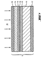
- a semiconductor 12 which preferably has a surface with a roughness factor> 1, is applied as a light-absorbing layer on a conductive carrier 11, which can serve as an electrode or contact and consists, for example, of a metal or indium tin oxide (ITO).
- the cell according to the invention preferably contains a chromophore on the surface of the semiconductor, shown here as chromophore layer 13.
- the term light-absorbing layer encompasses both a semiconductor layer and a combination of semiconductor / chromophore, even if the actual absorption in this case takes place almost exclusively by the chromophore.
- the charge transport layer 14 which according to the invention contains a hole conductor material of the formula (I). It is delimited on one side by the counterelectrode 15, which can consist, for example, of a conductive glass, conductively coated plastic, metal or another conductive, preferably translucent material.
- the cell 1 is preferably closed at the top and bottom by an insulating layer 16 and 17, respectively. It can contain a side closure, not shown in the figure, for example a frame made of an electrically insulating material, such as plastic or glass. However, by using a hole conductor material instead of the liquid electrolyte, such a side frame is not fundamentally necessary. At least one side of the cell must be transparent to the light to be converted into electrical energy, so that it can reach the chromophore or the semiconductor.
- the cell according to the invention also contains devices, not shown in the figure, for taking off the electrical current generated by the cell.
- a hole conductor material in the sense of the invention is a material that is positive Can conduct charge, which is caused by the absence of an electron, wherein Mass transport and cargo transport are decoupled.
- electron-rich, preferably organic compounds are suitable, which are oxidizable, preferably reversible. It is generally believed that the charge transport in an organic hole conductor material over the Radical cations are formed.
- the oxidation potential is variable over a wide range and can be attributed to adapted to specific energy levels of the semiconductor or sensitizer become. It is preferably between the energy level of the ground state and 700, preferably 400, particularly preferably 300, mV above the Ground state.
- Hole conductor materials in which no mass transport takes place or in which charge and mass transport are completely decoupled are preferred. Solid, in particular amorphous, hole conductor materials of the formula (I) are also preferred.
- Hole conductor layer can be prepared amorphously, i.e. in the amorphous state in the photovoltaic cell according to the invention is applied.
- Amorphous is used to describe the state of solids, their molecular ones Building blocks are not arranged in crystal lattices, but randomly. Different from in a crystal in which a short-range order (i.e. constant Distances to nearest neighboring atoms) and a long-range order (regular Repetition of a basic grid) exists, there is only one in the amorphous state Short-range order.
- the amorphous substance has no physically excellent Direction; it isotropic. All amorphous substances strive to different degrees energetically more favorable crystalline state.
- X-ray diffraction There are no electron and neutron beams in the amorphous solid sharp interference rings, like a crystal, but only diffuse Interference rings at small diffraction angles (halos).
- the amorphous state is thus clear from crystalline, liquid or too liquid crystal state differentiated.
- Hole conductor materials which are in organic Solvents are soluble, as well as hole conductor materials that are meltable.
- organic solvents to which the invention is not based are restricted are chloroform, benzene, chlorobenzene, cyclohexanone, toluene, Tetrahydrofuran, anisole, cresol, xylene, methyl lactate, methylene chloride, hexane, or other aliphatic, aromatic or alcoholic solvents. It is enough for the production of a hole conductor layer according to the invention, if that Hole conductor material is soluble or meltable in an organic solvent is.
- Soluble in the sense of the invention means a solubility of at least 1.0 g / l at 25 ° C in an organic or inorganic Solvent, preferably in one of the solvents listed above.
- Hole conductor materials based on their size are also particularly preferred can diffuse into the pores of a rough semiconductor layer.
- the molecules of the hole transport layer have a comparable molecular dimension to the molecules of the sensitizer, if used, so that the hole conductor molecules can come into close contact with the sensitizer molecules located in the pores of the semiconductor surface.
- the hole conductor molecules are particularly preferably larger than the factor 20, very particularly preferably 10, larger than corresponding sensitizer molecules.
- Hole conductor materials are very particularly preferred in which the voltage loss across the hole conductor layer when irradiated with sunlight is ⁇ 500 mV, preferably ⁇ 50 mV, particularly preferably ⁇ 20 mV.
- the hole conductor layer generally has a thickness of 0.1 to 20, preferably 1 to 15 ⁇ m.
- the charge carrier mobility of the hole conductor material is preferably at least 10 -5 cm 2 / Vs, in particular 10 -3 to 10 cm 2 / Vs.
- Spiro compounds are compounds in which two ring systems are linked by a single, four-bonded atom. This atom is called spiro atom, as in the Handbook of Chemistry and Physics 62 nd ed. (1981-2), CRC Press, pp C-23 to C-25 is executed.
- spiro compound means monomeric and polymeric carbospiro and heterospiro compounds.
- Preferred compounds of the formula (III) are those of the formula (IIIa) - (IIIg)
- Particularly preferred spiro compounds of the formula (IV) are 2,2 ', 4,4', 7,7'-hexakis (biphenylyl) -9,9'-spirobifluorene, 2,2 ', 4,4', 7,7'-hexakis (terphenylyl) -9,9'-spirobifluorene, 2,2 ', 4,4'-hexakis (biphenylyl) -9,9'-spirobi-9-silafluorene and 2,2 ', 4,4'7,7'-hexakis (terphenylyl) -9,9'-spirobi-9-silafluorene.
- the preparation of compounds of formula (IIIa) can for example starting from a tetrahalogenation in positions 2.2 ', 7.7' of the 9,9'-spirobifluorene followed by a substitution reaction (see e.g. US 5,026,894) or via a tetraacetylation of positions 2.2 ', 7.7' of 9,9'-spirobifluorene with subsequent C-C linkage Conversion of acetyl groups into aldehyde groups or heterocycle structure after conversion of the acetyl groups into carboxylic acid groups.
- the preparation of compounds of the formula (IIIc) can be carried out, for example, via a dibromination in 2.2 'position and subsequent diacetylation in 7.7' Position of 9,9'-spirobifluorene and subsequent implementation analogous to that of the compounds (IIIa).
- disubstituted pyridines disubstituted pyrazines, disubstituted pyrimidines and disubstituted pyridazines are found for example in the corresponding volumes of the series "The Chemistry of Heterocyclic Compounds "by A. Weissberger and E. C. Taylor (Editor).
- Heterospiro compounds of the formula (IIIa) can be prepared, for example, from a tetrahalogenation in positions 2,2 ', 7,7' of 9,9'-spirobi-9-silafluorene and subsequent substitution reaction, which is known from analogous C-spiro compounds (see, for example, US Pat. No. 5,026,894) or via a tetraacetylation of positions 2,2 ', 7,7' of 9,9'-spirobi-9-silafluorene with subsequent CC linkage after conversion of the acetyl groups into aldehyde groups or heterocycle formation after conversion of the acetyl groups into Carboxylic acid groups take place.
- the preparation of compounds of the formula (IIIc) can be carried out, for example, via a dibromination in the 2,2'-position with subsequent diacetylation in 7,7'-position of 9,9'-spirobi-9-silafluorene and subsequent reaction analogous to that of the compounds (IIIa).
- the photovoltaic cell according to the invention preferably contains, as the light-absorbing layer, a semiconductor which preferably has a very large band gap, particularly preferably at least 3.0 eV, very particularly preferably above 3.0 eV.
- Metal oxide semiconductors in particular the oxides of the transition metals, and the elements of the third main group and the fourth, fifth and sixth subgroup (the periodic system of the elements) of titanium, zirconium, hafnium, strontium, zinc, indium, yttrium, are therefore preferably suitable.
- perovskites such as SrTiO 3 , CaTiO 3
- oxides of other metals of the second and third main group or mixed oxides or oxide mixtures of these metals can also be used.
- Titanium dioxide is particularly preferred as the semiconductor material.
- the semiconductor preferably has a roughness factor of greater than 1, particularly preferably greater than 20, very particularly greater than 150.
- the roughness factor is defined as the ratio of an actual / effective surface to the area of the projection of this surface of a body, in this case the surface of the semiconductor.
- the roughness factor can be determined, for example, by gravimetric adsorption methods be determined, e.g. in F. Kohlrausch, Practical Physics, Volume 1, P. 397 (Stuttgart: B.G. Teubner, 1985). In general the size of the pores is 5-200 nm, preferably 10-50 nm.
- a method for producing polycrystalline metal oxide semiconductor layers using the SOL-GEL method (described in detail, for example, in Stalder and Augustynski, J. Electrochem. Soc. 1979, 126, 2007), where in the method step the hydrolysis of the metal Alcoholate, the percentage relative humidity of the ambient atmosphere can be in a range from 30% to 80% and is kept constant within ⁇ 5%, preferably ⁇ 1%, results in metal oxide semiconductor layers with which a particularly high electrical yield is achieved in photovoltaic cells according to the invention can be achieved.
- the rough surface with a polycrystalline structure offers an area which is larger by the roughness factor for a, preferably, monomolecular surface layer of the chromophore.
- the semiconductor can be considered transparent to the incident luminous flux.
- light is partially reflected on the surface and reaches e.g. T. on neighboring surfaces.
- the penetrating into the semiconductor and not absorbed or converted light hits z. T. directly and partly indirectly and partly indirectly, after total reflection on the surface on the exit side of chromophore molecules, which makes it possible to achieve a significantly higher luminous efficiency.
- the SOL-GEL process is described below as an example.
- the titanium substrate of pure titanium of approximately 99.5% purity is first cleaned in approximately 18% boiling HCl over approximately 30 minutes.
- the titanium ethoxide solution can e.g. B. be obtained by the solution of 21 mmol of TiCl 4 in 10 ml of very pure ethanol (puriss.). This solution is then diluted with very pure methanol (puriss.) To obtain a titanium concentration in the range of about 25 to 50 mg / ml.
- a drop of the solution is added to the titanium substrate and the titanium alkoxide is hydrolyzed at room temperature for about 30 minutes at a humidity of 48 ⁇ 1%.
- the substrate with the hydrolyzed layer is then heated to about 450 ° C. for about 15 minutes. This process is repeated several times. After repeating 10 to 15 times, the TiO 2 layer has reached a thickness of approximately 20 ⁇ m.
- the substrate with the layer is then baked at about 500 ° C. for about 30 minutes in a pure argon atmosphere (for example 99.997%).
- the TiO 2 layer produced in this way has a roughness factor in the range of 200.
- Metal oxide semiconductor layers of this type can be produced on other substrates using analog processes.
- the upper layers of the semiconductor can optionally, such as. B. described in WO-A 91/16719, doped with a divalent or trivalent metal.
- the sensitivity that is to say the photoelectronic yield for visible light, that is to say also for sunlight, can be increased by so-called chromophores, also known as sensitizers or dyes, being chemically attached or incorporated (chemisorbed) as charge carriers on the surface of the semiconductor.
- chromophores also known as sensitizers or dyes
- the two functions of light absorption and charge carrier separation are separated in these photoelectronic systems.
- the light absorption is taken over by the chromophore in the surface area, and the charge carriers are separated at the semiconductor / chromophore interface.
- Different chromophores have different spectral sensitivities. The choice of the chromophore can thus be adapted to the spectral composition of the light from the light source in order to increase the yield as much as possible.
- the complexes of transition metals of the type metal (L 3 ), metal (L 2 ) of ruthenium and osmium are suitable as chromophores, ie sensitizers, Ruthenium cis diaqua bipyridyl complexes, such as ruthenium cis-diaqua bis (2,2 bipyridyl-4,4'dicarboxylate) as well as porphyrins (e.g. zinc tetra (4-carboxyphenyl) porphyrin) and cyanides (e.g.
- the chromophores can be chemisorbed, adsorbed or otherwise firmly attached in the area of the surface of the metal oxide semiconductor.
- Favorable results have been achieved, for example, with chromophores which are bound to the surface of the metal oxide semiconductor using carboxylic acid or phosphonic acid ligands.
- Suitable chromophores are, for example, also in Chem. Rev. 1995, 49-68 described.
- Chromophores (VIII) and (IX) are particularly preferred, their synthesis and properties in J. Chem. Soc. Chem. Comm. 1995, 65 are described.
- chromophore for example RuL 3 4- , z. B. by immersing the substrate with the oxide layer in an ethanolic solution of 2 x 10 -4 M RuL 3 4- , for about an hour.
- Other chromophores can be applied to titanium oxide or other metal oxide semiconductors using analog processes.
- Stable, metallically conductive substances for. B. Au, Ag, Pt, Cu, or other metals. But it can also, for some applications preferably translucent conductive substances, such as doped metal oxides, z. B. indium tin oxide, Sb-doped tin oxide or Al-doped zinc oxide, be used.
- the work function of the used Electrode material preferably to the ionization potential of the used Hole transport material can be adjusted.
- the electrode can, as described in EP-A 0 333 641, on a transparent substrate, e.g. B. glass, and with the Hole transport layer to be connected.
- a transparent substrate e.g. B. glass
- it can in this Invention described cell by physical deposition methods, e.g. B. Evaporation or atomization (sputtering) directly onto the hole transport layer can be applied without the need for a second glass plate. This Procedure is preferred in applications when the weight of the cell should be reduced.
- the electrode can also, as in WO-A 93/19479 described, be coated with another semiconductor.
- electrically insulating materials 16 and 17 or optionally as Lateral frames for the cell according to the invention are suitable, for example Plastic or glass.
- the cell can e.g. B. sealed with an adhesive or a film become.
- the photovoltaic cell according to the invention generally has a thickness of 5 to 20 mm (with substrate). To avoid reflection losses, it can be provided with a one, two or more layers of anti-reflective coating.
- the rear of the cell can be designed to increase the light output be that light is diffusely reflected back into the cell.
- a further increase in the luminous efficacy can be achieved in this way, for example be that the incident sunlight, for example through mirrors or Fresnel lens is concentrated.
- the cell according to the invention can also be part of a tandem cell; in such Devices convert light from different sub-cells Spectral ranges into electrical energy.
- the cell according to the invention is used as a photocell, i. that is, it is used for Generating electrical energy from light. It is preferably a solar cell, d. H. a device for generating electrical energy Sunlight.
- Compound 1 described in Example 3 was dissolved in tetrahydrofuran at a concentration of 50 g / l.
- a substrate was coated by immersion in the solution, said substrate consisting of conductive, SnO 2 -coated glass, on which a smooth layer of Nb-doped titanium dioxide had been applied on one side (substrate I). Both sides of the substrate were coated by an immersion process.
- a thin layer of gold was then deposited on the side coated with titanium dioxide by thermal evaporation.
- the side coated with titanium dioxide and gold is hereinafter referred to as the active side, the other as the inactive side.
- the sample prepared in this way was mounted in an optical assembly that consists of a high pressure lamp, optical filters, lenses and brackets. By using filters and moving the lenses, the Intensity can be varied. Furthermore, the light became wavelength below of 380 nm essentially filtered out to provide a direct excitation from Prevent connection 1 by light.
- the sample was inactive with the Mounted side facing the lamp so that the residual light in the area of Absorption spectrum of compound 1 on the inactive side layer was absorbed. By doping with Nb, the Titanium dioxide layer has a low absorption between 400 and 450 nm, so that this was stimulated by the lamp.
- the gold and SnO 2 layers were contacted and connected to an ammeter while the sample was exposed. No external voltage was applied. A current was observed during the exposure of the sample, which disappeared after the light source was dimmed. When compared to a thermal treatment of the sample, it was shown that the current observed was a real photocurrent generated by injecting positive charge carriers (holes) into the compound 1 layer and transporting the holes through this layer. The intensity of the exposure was varied by a factor of ten; Over this range the photocurrent grew linearly with the intensity.
- Compound 1 was dissolved in tetrahydrofuran at a concentration of 50 g / l.
- a substrate was coated, which consisted of conductive, SnO 2 -coated glass, on which a nanoporous layer of titanium dioxide had been applied on one side, the proportion of the rutile phase still weakly absorbing above 400 nm being about 30% and the surface had a roughness factor of 700-1000 (substrate II). Both sides of the substrate were coated by an immersion process.
- a thin layer of gold was then applied to the side coated with titanium dioxide by thermal evaporation.
- the side coated with titanium dioxide and gold is hereinafter referred to as the active side, the other as the inactive side.
- the sample thus prepared was in the optical described in Example 7 Structure assembled.
- the sample was directed towards the lamp with the inactive side mounted so that the residual light in the range of the absorption spectrum Compound 1 absorbed by the layer on the inactive side has been. Due to the proportion of the rutile phase, the titanium dioxide layer had one low absorption between 400 and 430 nm, so that this from the lamp was stimulated.
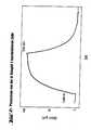
- the gold and SnO 2 layers were contacted and connected to an ammeter while the sample was exposed. No external voltage was applied. A current was observed during the exposure of the sample, which disappeared after the light source was dimmed. A comparison of the thermal treatment of the sample showed that the observed current was a real photocurrent which is produced by injecting positive charge carriers (holes) into the layer from compound 1 and transporting the holes through this layer. The intensity of the exposure was varied by a factor of ten; Over this range the photocurrent grew linearly with the intensity. The photocurrent was many times higher than the photocurrent of the sample described in Example 7, which indicates that compound 1 penetrates into the pores of the layer (see FIG. 2).
- Example 7 The sample described in Example 7 was mounted in an optical setup, that of a pulsed, tunable laser, a white light source, one Monochromator and imaging and detection optics existed.
- the laser delivered pulses at 30 Hz with a duration of approx. 2 ns at 420 nm, i.e. outside of the absorption of compound 1, but still within the Absorption of the Nb-doped titanium dioxide layer. While the sample is irradiated like this the transient absorption of the radical cation of compound 1 observed at 500 nm. The increase in absorption took place within the Time resolution of the experiment instead. This indicates a very effective and rapid injection of the charge carriers into the layer from compound 1.
- a nanoporous layer of TiO 2 was applied to an SnO 2 -coated glass support by screen printing with a suspension produced by the sol-gel method and dried in a hot air stream at approx. 400 ° C. for approx. 20 minutes.
- the layer thickness is about 1.5 ⁇ m, the layer consists almost entirely of the anatase phase and therefore has no absorption above 400 nm.
- the coated support was immersed in a 10 -4 M ethanolic solution of ruthenium tris (2,2'bipyridyl-4,4'-dicarboxylate) at a temperature of approx. 50 ° C. After approximately 2 hours, the carrier was removed from the solution, rinsed with ethanol and briefly dried in a warm air stream.
- the layer system had a maximum absorbance of approximately 0.2 at approximately 500 nm. The area of the sample was approx. 0.3 cm 2 .
- the sample thus prepared was assembled in the structure described in Example 7.
- the light with a wavelength below 430 nm was blocked by using appropriate optical filters.
- the structure was adjusted so that the intensity of the radiation corresponded approximately to the intensity of sunlight in Central Europe (approx. 750 W / m 2 ).
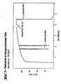
- the gold and SnO 2 layers were contacted and connected to a potentiostat while the sample was exposed. Without external voltage, the sample showed a current of approx. 200 nA under exposure, but no current without exposure. When an edge filter was installed at 470 nm, the decrease in photocurrent corresponded approximately to the decrease in light absorption by the dye (see FIG. 3).
- the current-voltage characteristics of the sample were measured with and without exposure. Without exposure, no more measurable current flowed, even when external voltage was applied.
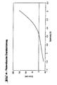
- the characteristics of a photovoltaic cell with an open circuit voltage of approximately 500-600 mV and a short-circuit current of approximately 800 nA / cm 2 were measured under exposure (see FIG. 4).
- a nanoporous layer of TiO 2 was applied to an SnO 2 -coated glass support by screen printing with a suspension produced by the sol-gel method and dried in a hot air stream at approx. 400 ° C. for approx. 20 minutes.
- the layer thickness is about 1.5 ⁇ m, the layer consists almost entirely of the anatase phase and therefore has no absorption above 400 nm.
- the coated support was immersed in a 10 -4 M ethanolic solution of ruthenium tris (2,2'bipyridyl-4,4'-dicarboxylate) at a temperature of approx. 50 ° C. After approximately 2 hours, the carrier was removed from the solution, rinsed with ethanol and briefly dried in a warm air stream.
- the layer system had a maximum absorbance of approximately 0.2 at approximately 500 nm. The area of the sample was approx. 0.3 cm 2 .
- the sample thus prepared was assembled in the structure described in Example 7.
- the light with a wavelength below 430 nm was blocked by using appropriate optical filters.
- the structure was adjusted so that the intensity of the radiation corresponded approximately to the intensity of sunlight in Central Europe (approx. 750 W / m 2 ).
- the gold and SnO 2 layers were contacted and connected to a potentiostat while the sample was exposed. Without external voltage, the sample showed a current of approx. 7 ⁇ A when exposed, without exposure no current.
- the current-voltage characteristics of the sample were measured with and without exposure. Without exposure, no more measurable current flowed, even when external voltage was applied.
- the characteristics of a photovoltaic cell with an open circuit voltage of approx. 500 mV and a short circuit current of approx. 14 ⁇ A / cm 2 were measured under exposure.
Landscapes
- Chemical & Material Sciences (AREA)
- Organic Chemistry (AREA)
- Physics & Mathematics (AREA)
- Engineering & Computer Science (AREA)
- Materials Engineering (AREA)
- Spectroscopy & Molecular Physics (AREA)
- Inorganic Chemistry (AREA)
- Electromagnetism (AREA)
- Photovoltaic Devices (AREA)
- Hybrid Cells (AREA)
- Heterocyclic Carbon Compounds Containing A Hetero Ring Having Oxygen Or Sulfur (AREA)
Abstract
Description
Handelt es sich um Sonnenlicht, spricht man von einer Solarzelle.
Obwohl der photovoltaische Effekt, d. h. das Auftreten einer Spannung über einem pn-Übergang bei Einstrahlung von Licht, bereits 1893 von Becquerel beobachtet wurde, gelang es erst mit der Entwicklung der Halbleitertechnik in den vierziger und fünfziger Jahren dieses Jahrhunderts, die ersten funktionsfähigen Solarzellen herzustellen.
Die heute verwendeten Solarzellen enthalten üblicherweise als lichtabsorbierende Schicht ein Halbleitermaterial, in den meisten Fällen Silicium, das für diese Anwendung allerdings höchsten Ansprüchen an die Reinheit und Qualität der Verarbeitung genügen muß. Dadurch sind Solarzellen heute bei vielen Anwendungen aus Kostengründen nicht konkurrenzfähig.
Demgegenüber wird in einer Farbstoff-sensibilisierten Solarzelle, wie sie in den sechziger Jahren von H. Tributsch entwickelt wurde, als Halbleiter ein Material mit sehr großer Bandlücke, wie Titandioxid, verwendet. Ein solcher Halbleiter absorbiert das Sonnenlicht nur wenig, hierfür wird auf den Halbleiter ein Farbstoff (Chromophor) aufgetragen.
Obwohl mit solchen Zellen gute Ergebnisse erzielt werden, ist das Eigenschaftsprofil einer solchen Vorrichtung noch deutlich verbesserungsfähig.
Insbesondere nachteilig ist, daß das Elektron durch die Diffusion von Ionen an den Farbstoff zurückgeführt werden muß. Dadurch kommen nur Redoxsysteme in Frage, die klein genug sind, um in die Poren der nanokristallinen Halbleiterschicht einzudringen. Selbst bei dem bisher besten Redox-System, I2/I3 geht ungefähr 40 % der theoretisch zur Verfügung stehenden Energie als Wärme verloren, und der Wirkungsgrad für die Energiekonversion ist auf ca. 10 % im Sonnenlicht begrenzt. Zudem muß im Elektrolyt stets ein Kompromiß zwischen Viskosität und Mobilität der Ionen gefunden werden, der keiner der beiden Anforderungen ideal genügt.
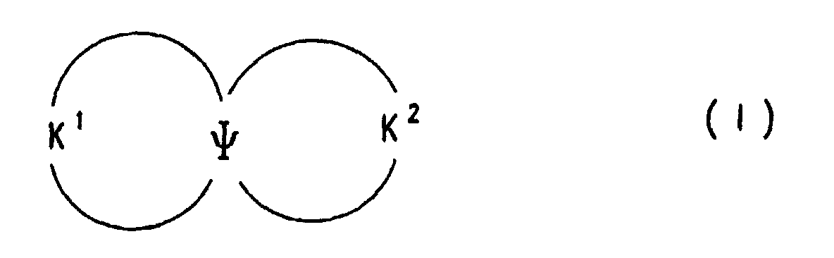
Ψ C, Si, Ge oder Sn, vorzugsweise C, Si oder Ge, besonders bevorzugt C oder
Si und insbesondere C und
K1 und K2 unabhängig voneinander konjugierte Systeme
bedeuten, als Lochleitermaterialien enthält.
Auf einem leitenden Träger 11, der als Elektrode bzw. Kontakt dienen kann und beispielsweise aus einem Metall oder Indium-Zinn-Oxid (ITO) besteht, ist als lichtabsorbierende Schicht ein Halbleiter 12 aufgebracht, der vorzugsweise eine Oberfläche mit einem Rauheitsfaktor > 1 hat. Vorzugsweise enthält die erfindungsgemäße Zelle auf der Oberfläche des Halbleiters einen Chromophor, hier als Chromophorschicht 13 dargestellt. Die Bezeichnung lichtabsorbierende Schicht umfaßt im Sinne der Erfindung sowohl eine Halbleiterschicht als auch eine Kombination Halbleiter/Chromophor, auch wenn die eigentliche Absorption in diesem Fall nahezu ausschließlich durch den Chromophor erfolgt. Daran schließt sich die Ladungstransportschicht 14 an, die erfindungsgemäß ein Lochleitermaterial der Formel (I) enthält. Sie wird auf der einen Seite durch die Gegenelektrode 15 begrenzt, die beispielsweise aus einem leitfähigen Glas, leitfähig beschichtetem Kunststoff, aus Metall oder einem anderen leitfähigen, vorzugsweise lichtdurchlässigen Material, bestehen kann. Die Zelle 1 ist vorzugsweise oben und unten durch je eine isolierende Schicht 16 bzw. 17 abgeschlossen. Sie kann einen, in der Figur nicht gezeigten seitlichen Abschluß enthalten, beispielsweise einen Rahmen aus einem elektrisch isolierendem Material, wie Kunststoff oder Glas. Durch die Verwendung eines Lochleitermaterials anstelle des flüssigen Elektrolyten ist solch ein seitlicher Rahmen aber nicht grundsätzlich notwendig. Zumindest eine Seite der Zelle muß für das in elektrische Energie zu wandelnde Licht durchlässig sein, so daß dieses zu dem Chromophor bzw. dem Halbleiter gelangen kann.
Die erfindungsgemäße Zelle enthält darüber hinaus in der Figur nicht gezeigte Vorrichtungen zur Abnahme des von der Zelle erzeugten elektrischen Stroms.
Weiterhin bevorzugt sind feste, insbesondere amorphe Lochleitermaterialien der Formel (I).
Die Lochleiterschicht weist im allgemeinen eine Dicke von 0,1 bis 20, vorzugsweise 1 bis 15 µm auf.
Die Ladungsträgerbeweglichkeit des Lochleitermaterials beträgt vorzugsweise mindetens 10-5 cm2/Vs, insbesondere 10-3 bis 10 cm2/Vs.


- R
- hat, gleich oder verschieden, die gleichen Bedeutungen wie K, L, M, N oder ist Wasserstoff, eine lineare oder verzweigte Alkyl-, Alkoxy- oder Carboalkoxygruppe mit 1 bis 22, vorzugsweise 1 bis 15, besonders bevorzugt 1 bis 12 C-Atomen, -CN, -NO2, -NR1R2, -Ar oder -O-Ar;
- Ar
- ist Phenyl, Biphenyl, 1-Naphthyl, 2-Naphthyl, 2-Thienyl, 2-Furanyl, wobei jede dieser Gruppen einen oder zwei Reste R tragen kann;
- m, n, p
- sind 0, 1, 2 oder 3;
- X, Y
- sind = CR- oder = N-;
- Z
- ist -O-, -S-, -NR-, -CRR-, -CH = CH-, -CH = N-;
- R1 und R2
- sind Wasserstoff, eine lineare oder verzweigte Alkylgruppe mit 1 bis 22 C-Atomen, -Ar oder 3-Methylphenyl.










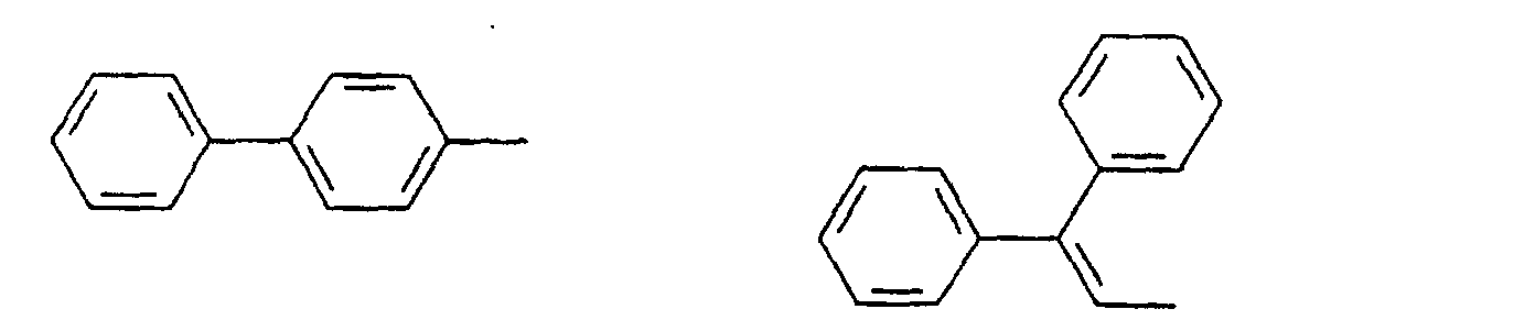






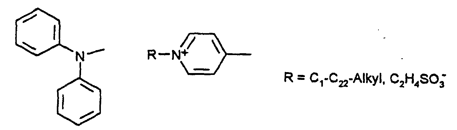


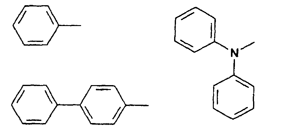

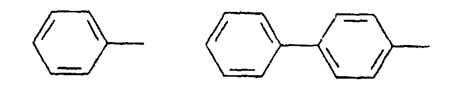
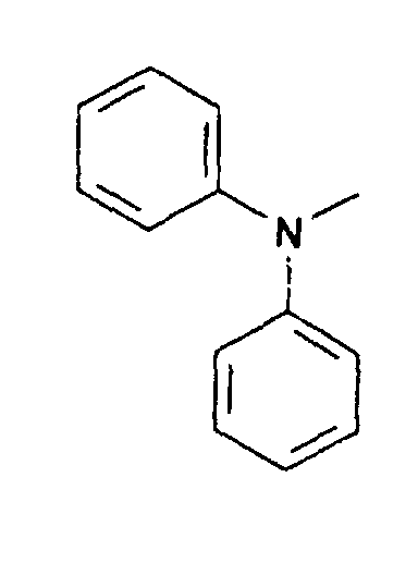

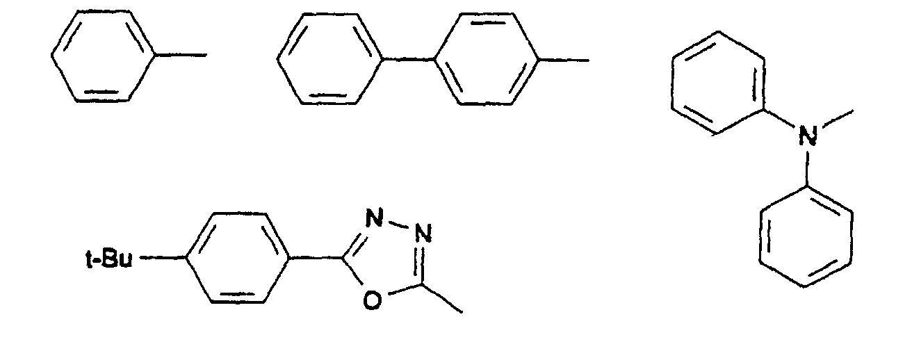
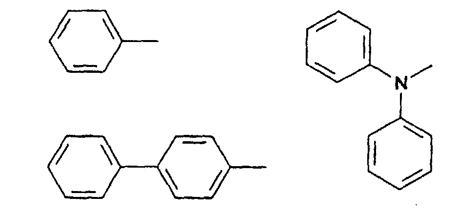





2,2',4,4',7,7'-Hexakis(biphenylyl)-9,9'-spirobifluoren,
2,2',4,4',7,7'-Hexakis(terphenylyl)-9,9'-spirobifluoren,
2,2',4,4'-Hexakis(biphenylyl)-9,9'-spirobi-9-silafluoren und
2,2',4,4'7,7'-Hexakis(terphenylyl)-9,9'-spirobi-9-silafluoren.
und 27 52 975 für Verbindungen mit 1,4-Phenylen-Gruppen;
DE-A 26 41 724 für Verbindungen mit Pyrimidin-2,5-diyl-Gruppen; DE-A 40 26 223 und EP-A 03 91 203 für Verbindungen mit Pyridin-2,5-diyl-Gruppen;
DE-A 32 31 462 für Verbindungen mit Pyridazin-3,6-diyl-Gruppen; N. Miyaura, T. Yanagi und A. Suzuki in Synthetic Communications 1981, 11, 513 bis 519, DE-A-39 30 663; M. J. Sharp, W. Cheng, V. Snieckus, Tetrahedron Letters 1987, 28, 5093; G. W. Gray, J. Chem. Soc. Perkin Trans II 1989, 2041 und Mol. Cryst. Liq. Cryst. 1989, 172, 165; Mol. Cryst. Liq. Cryst. 1991, 204, 43 und 91; EP-A 0 449 015; WO 89/12039; WO 89/03821; EP-A 0 354 434 für die direkte Verknüpfung von Aromaten und Heteroaromaten.

Die Herstellung von Verbindungen der Formel (IIIb) kann beispielsweise analog zu denen der Formel (IIIa) erfolgen, wobei die stöchiometrischen Verhältnisse bei der Umsetzung so gewählt werden, daß die Positionen 2,2' bzw. 7,7' funktionalisiert werden (siehe z.B. J. H. Weisburger, E. K. Weisburger, F.E. Ray, J. Am. Chem. Soc. 1959, 72, 4253; F.K. Sutcliffe, H. M. Shahidi, D. Patersor., J. Soc. Dyers Colour 1978, 94, 306 und G. Haas, V. Prelog, Helv. Chim. Acta 1969, 52, 1202).


DE-A 196 06 511; DE-A 196 14 971 und DE-A 196 15 128 beschrieben; auf diese Schriften wird hiermit ausdrücklich Bezug genommen, ihre Offenbarung gilt durch Zitat als Bestandteil der vorliegenden Anmeldung.
Damit eignen sich vorzugsweise Metalloxyd-Halbleiter, insbesondere die Oxyde der Übergangsmetalle, sowie der Elemente der dritten Hauptgruppe und der vierten, fünften und sechsten Nebengruppe (des periodischen Systems der Elemente) von Titan, Zirkon, Hafnium, Strontium, Zink, Indium, Yttrium, Lanthan, Vanadium, Niob, Tantal, Chrom, Molybdän, Wolfram, aber auch Oxyde von Zink, Eisen, Nickel oder Silber, Perovskite wie SrTiO3, CaTiO3, oder Oxyde von anderen Metallen der zweiten und dritten Hauptgruppe oder Mischoxyde oder Oxydgemische dieser Metalle. Es kann aber auch jedes andere Metalloxyd mit Halbleitereigenschaften und großem Energieabstand (Bandlücke) zwischen Valenzband und Leitungband verwendet werden.
Besonders bevorzugt als Halbleitermaterial ist Titandioxid.
Der Rauheitsfaktor ist definiert als das Verhältnis einer wirklichen/effektiven Oberfläche zur Fläche der Projektion dieser Oberfläche eines Körpers, in diesem Fall also der Oberfläche des Halbleiters.
Die rauhe Oberfläche mit polykristalliner Struktur bietet eine um den Rauheitsfaktor größere Fläche für eine, vorzugsweise, monomolekulare Oberflächenschicht des Chromophors. Damit wird erreicht, daß das auf eine Fläche bestimmter Größe einfallende Licht mit bedeutend höherer Ausbeute in elektrische Energie gewandelt wird. Der Halbleiter kann als für den einfallenden Lichtstrom durchsichtig betrachtet werden. Licht wird aber teilweise auf der Oberfläche reflektiert und gelangt z. T. auf benachbarte Oberflächen. Das in den Halbleiter eindringende und nicht absorbierte bzw. gewandelte Licht trifft z. T. direkt und zu einem anderen Teil indirekt und zu einem weiteren Teil indirekt, nach Totalreflexion an der Oberfläche auf der Austrittsseite auf Chromophormoleküle, womit es gelingt, eine bedeutend höhere Lichtausbeute zu erzielen.
Das Titansubstrat aus reinem Titanium von etwa 99,5 % Reinheit wird zuerst während etwa 30 Minuten in etwa 18 %iger kochender HCI gereinigt. Die Titan-Ethoxyd-Lösung kann z. B. durch die Lösung von 21 mMol TiCl4 in 10 ml sehr reinem Ethanol (puriss.) erhalten werden. Diese Lösung wird dann mit sehr reinem Methanol (puriss.) verdünnt, um eine Titankonzentration im Bereich von etwa 25 bis 50 mg/ml zu erhalten. Auf das Titansubstrat gibt man einen Tropfen der Lösung und das Titan-Alkoxyd wird bei Raumtemperatur während ca. 30 Minuten bei einer Feuchtigkeit von 48 ± 1 % hydrolisiert. Danach wird das Substrat mit der hydrolysierten Schicht während ca. 15 Minuten auf ca. 450°C erhitzt. Dieser Prozeß wird mehrmals wiederholt. Nach 10- bis 15-maliger Wiederholung hat die TiO2-Schicht eine Dicke von etwa 20 µm erreicht.
Danach wird das Substrat mit der Schicht bei etwa 500°C während etwa 30 Minuten in einer Rein-Argon-Atmosphäre (z. B. 99,997 %) ausgeheizt. Die so hergestellte TiO2-Schicht hat einen Rauheitsfaktor im Bereich von 200. Derartige Metalloxyd-Halbleiter-Schichten (auch anderer Metalle) können nach analogen Verfahren auf anderen Substraten erzeugt werden. Die oberen Schichten des Halbleiters können gegebenenfalls, wie z. B. in der WO-A 91/16719 beschrieben, mit einem divalenten oder trivalenten Metall dotiert sein.
Verschiedene Chromophore haben unterschiedliche spektrale Empfindlichkeiten.
Die Wahl des Chromophors kann somit der spektralen Zusammensetzung des Lichts der Lichtquelle angepaßt werden, um die Ausbeute möglichst zu vergrößern. Als Chromophore, d. h. Sensibilisatoren, eigenen sich insbesondere die Komplexe von Übergangsmetallen vom Typ Metall (L3), Metall (L2) von Ruthenium und Osmium (z. B. Ruthenium tris (2,2 bipyridyl-4,4'dicarboxylate), Ruthenium cis diaqua bipyridyl Komplexe, wie Ruthenium cis-diaqua bis(2,2 bipyridyl-4,4'dicarboxylate) sowie Porphyrine (z. B. Zink tetra (4-carboxyphenyl) Porphyrin) und Cyanide (z. B. Eisen-Hexacyanid-Komplexe) und Phthalocyanine.
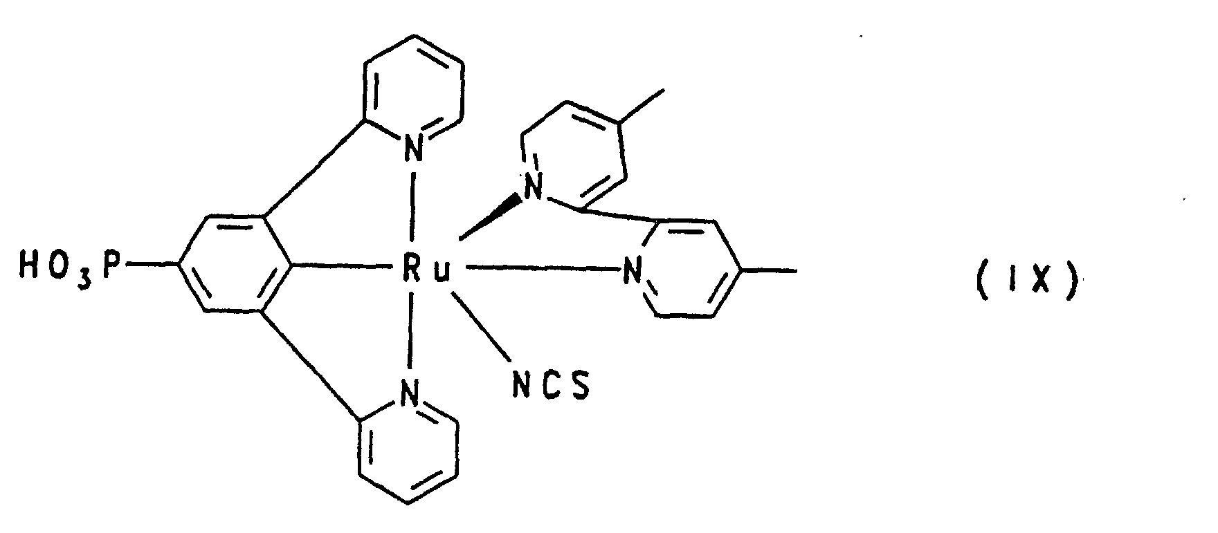
Die Chromophore können im Bereich der Oberfläche des Metalloxyd-Halbleiters chemisorbiert, adsorbiert oder sonstwie fest angelagert sein. Günstige Resultate wurden beispielsweise mit Chromophoren erzielt, die mit Carbonsäure- oder Phosphonsäure-Liganden an die Oberfläche des Metalloxyd-Halbleiters gebunden sind.

Sie kann zur Vermeidung von Reflexionsverlusten mit einer ein-, zwei- oder mehrlagigen Antireflexschicht versehen sein.
1H-NMR (CDCI3, ppm): 6.98 (d, J = 1,48 Hz, 4 H, H-1,1',8,8'); 7.54 (dd, J = 7.88, 1.48 Hz, 4 H, H-3,3',6,6'); 7.72 (d, J = 7.88 Hz, 4 H, H-4,4',5,5').
1H-NMR (CDCl3, ppm): 6.69 (d, J = 1,83 Hz, 4 H, H-1,1 ',8,8'); 6.92 (dd, J = 8.18, 1.99 Hz, 4 H, H-3.3',6,6'); 6.98 (m, 24 H}; 7.20 (m, 16 H); 7.45 (d, J = 8.18 Hz, 4 H, H-4,4',5,5').
1H-NMR (CDCl3, ppm): 3.76 (s, 24 H, OCH3); 6.54 (d, J = 1,99 Hz, 4 H, H-1,1',8,8'); 6.75 (dm, J = 9.07 Hz,16 H); 6.79 (dd, J = 8.18, 1.99 Hz, 4 H, H-3,3',6,6'); 6.90 (dm, J = 9.07 Hz, 16 H); 7.35 (d, J = 8.18 Hz, 4 H, H-4,4',5,5').
Das Schichtsystem wies eine maximale Absorbanz von ca. 0,2 bei ca. 500 nm auf. Die Fläche der Probe betrug ca. 0,3 cm2.
Das Schichtsystem wies eine maximale Absorbanz von ca. 0,2 bei ca. 500 nm auf. Die Fläche der Probe betrug ca. 0,3 cm2.
Claims (10)
- Photovoltaische Zelle, dadurch gekennzeichnet, daß als Ladungstransportschicht eine oder mehrere Spiroverbindungen der Formel (I) als Lochleitermaterialenwobei

- ψ
- C, Si, Ge oder Sn, vorzugsweise C, Si, Ge, besonders bevorzugt C, Si und insbesondere C, und
- K1 und K2
- unabhängig voneinander konjugierte Systeme
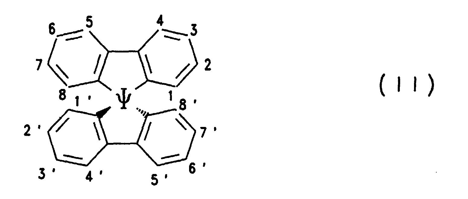
- Photovoltaische Zelle nach Anspruch 1, dadurch gekennzeichnet, daß als Lochleitermaterial ein oder mehrere 9,9'-Spirobifluorenderivate der Formel (II)wobei ψ in Formel (I) in Anspruch 1 angegebenen Bedeutungen hat und die Benzogruppen unabhängig voneinander substituiert und/oder anelliert sein können, verwendet werden.

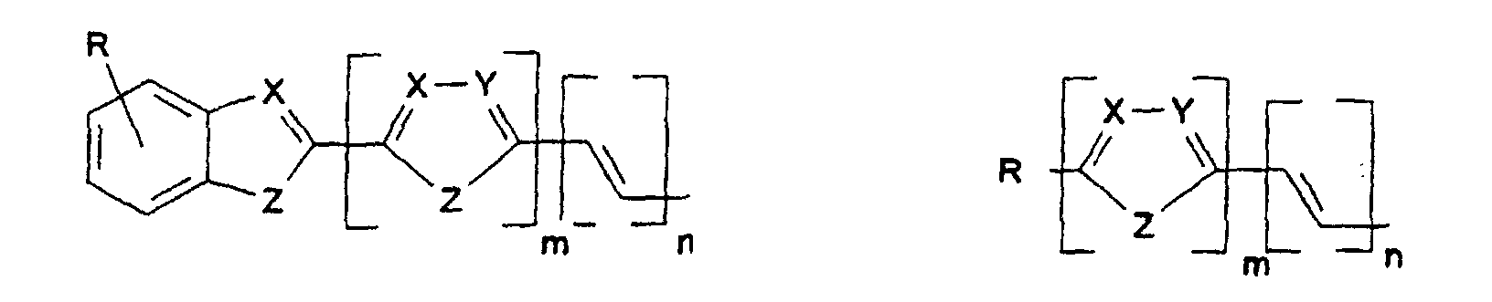
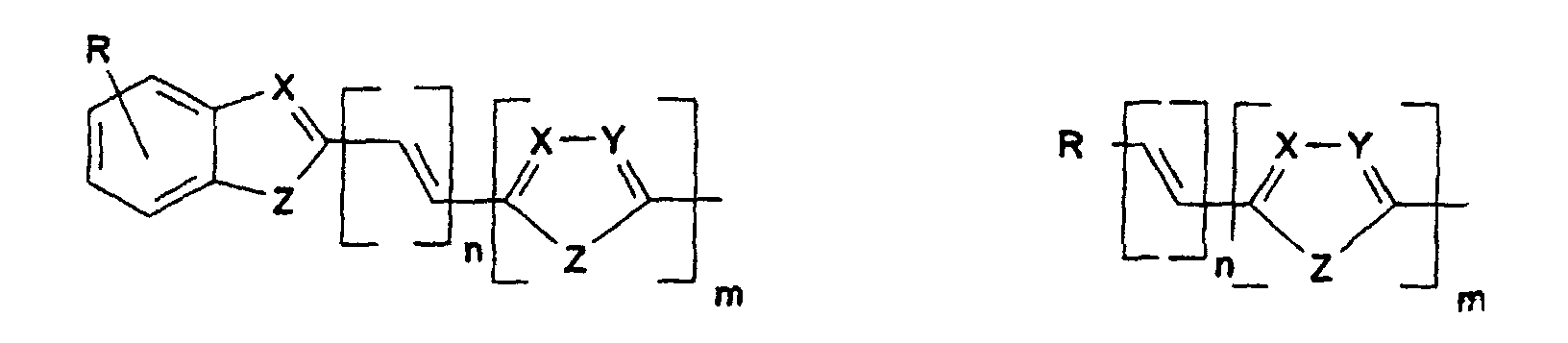
- Photovoltaische Zelle nach Anspruch 2, dadurch gekennzeichnet, daß als Lochleitermaterial ein oder mehrere Spirobifluorenderivate der Formel (III),wobei die Symbole und Indizes folgende Bedeutungen haben:
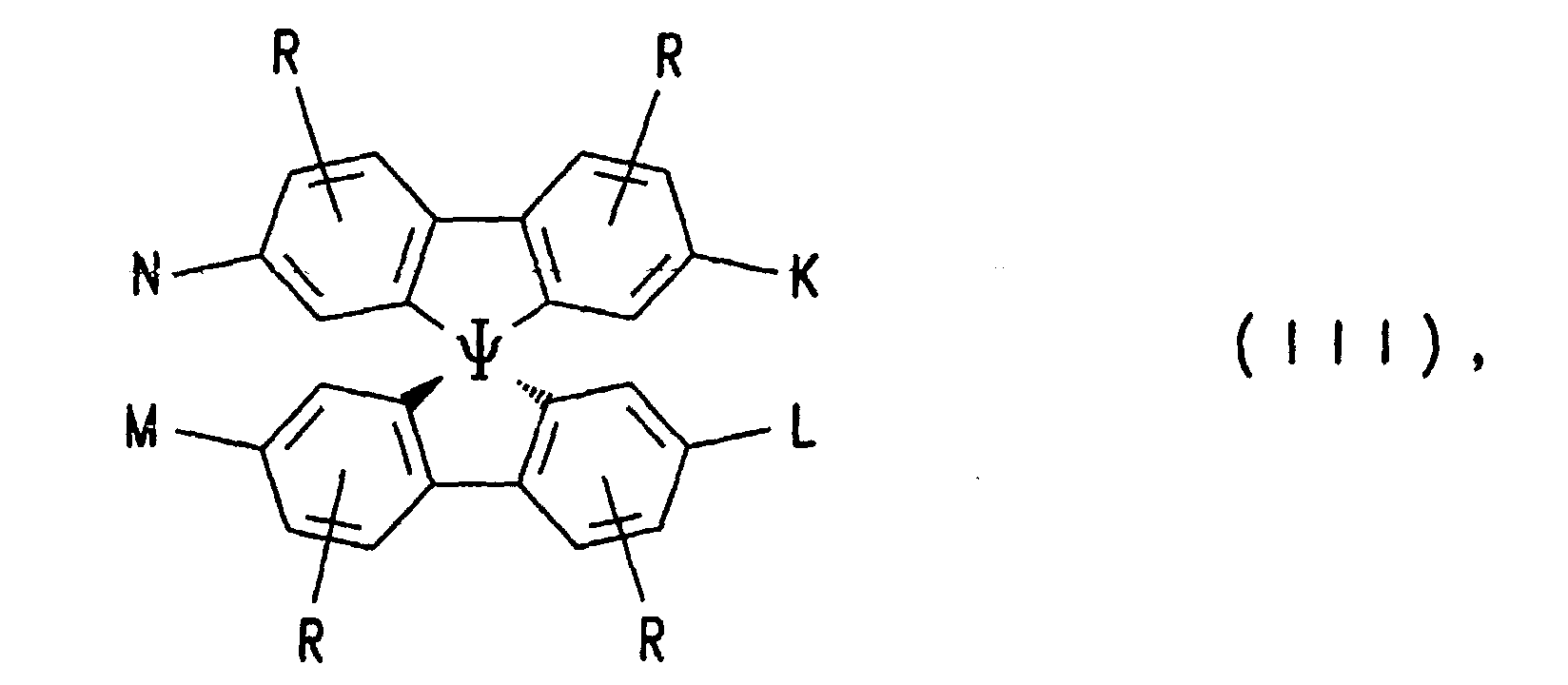
- ψ
- ist C, Si, vorzugsweise C,
- K, L, M, N
- sind gleich oder verschieden
und bedeuten eine Gruppe der Formeln
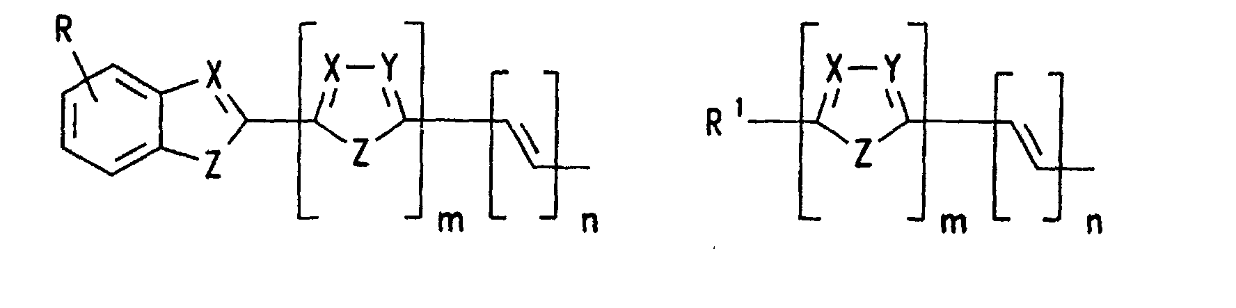
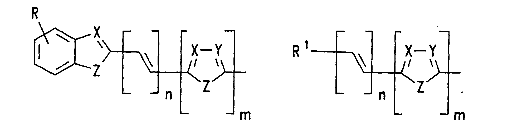
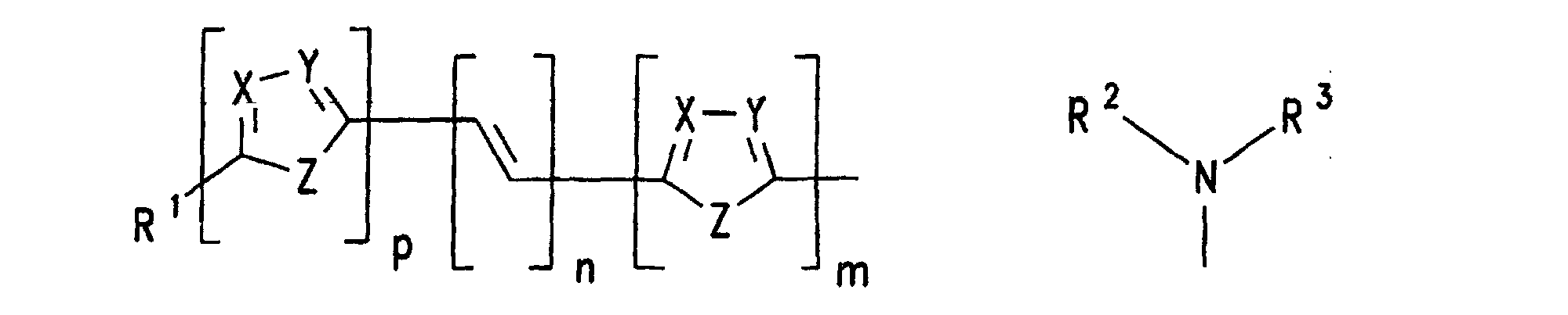
- R
- kann, gleich oder verschieden, die gleichen Bedeutungen wie K, L, M, N haben oder ist -H, eine lineare oder verzweigte Alkyl, Alkoxy oder Estergruppe mit 1 bis 22, vorzugsweise 1 bis 15, besonders bevorzugt 1 bis 12 C-Atomen, -CN, -NR2R3, -Ar oder -O-Ar;
- Ar
- ist Phenyl, Biphenyl, 1-Naphthyl, 2-Naphthyl, 2-Thienyl, 2-Furanyl, 9-Anthryl, wobei jede dieser Gruppen einen oder zwei Reste R tragen kann;
- m, n, p
- sind 0, 1, 2 oder 3;
- X, Y
- sind gleich oder verschieden CR oder Stickstoff;
- Z
- ist -O-, -S-, -NR1-, -CR1R4-, -CH = CH-, -CH = N-;
- R1, R4
- können, gleich oder verschieden, die gleichen Bedeutungen wie R haben;
- R2, R3
- sind gleich oder verschieden H, eine lineare oder verzweigte Alkylgruppe mit 1 bis 22 C-Atomen, -Ar, 3-Methylphenyl,
- Photovoltaische Zellen nach einem oder mehreren der vorhergehenden Ansprüche, gekennzeichnet durch eine lichtabsorbierende Schicht,die ein Halbleitermaterial mit einer Bandlücke von mindestens 3 eV enthält.
- Photovoltaische Zelle gemäß Anspruch 4, dadurch gekennzeichnet, daß das Halbleitermaterial ein Metalloxid ist.
- Photovoltaische Zelle nach Anspruch 4 oder 5, dadurch gekennzeichnet, daß die Halbleiteroberfläche einen Rauhigkeitsfaktor von > 20 aufweist.
- Photovoltaische Zelle nach einem oder mehreren der vorhergehenden Ansprüche, dadurch gekennzeichnet, daß sie eine lichtabsorbierende Schicht mit einem Farbstoff als Sensibilisator enthält.
- Photovoltaische Zelle nach einem oder mehreren der vorhergehenden Ansprüche, dadurch gekennzeichnet, daß das Lochmaterial amorph vorliegt.
- Verfahren zur Herstellung einer photovoltaischen Zelle nach einem oder mehreren der Ansprüche 4 bis 8, dadurch gekennzeichnet, daß man auf einem leitfähigen festen Trägera) ein Halbleiterkolloid aufbringt,b) darauf gegebenenfalls einen Farbstoff aufbringt,c) darauf eine Transportschicht, enthaltend das besagte Lochleitermaterial, aufbringt,d) darauf eine Gegenelektrode aufbringt, und auf diesee) eine isolierende Schicht aufbringt.
- Verwendung von photovoltaischen Zellen nach einem oder mehreren der Ansprüche 1 bis 8 zur Erzeugung von Strom aus Sonnenlicht.
Applications Claiming Priority (3)
| Application Number | Priority Date | Filing Date | Title |
|---|---|---|---|
| DE19533850A DE19533850A1 (de) | 1995-09-13 | 1995-09-13 | Photovoltaische Zelle |
| DE19533850 | 1995-09-13 | ||
| PCT/EP1996/003944 WO1997010617A1 (de) | 1995-09-13 | 1996-09-09 | Photovoltaische zelle |
Publications (2)
| Publication Number | Publication Date |
|---|---|
| EP0850492A1 EP0850492A1 (de) | 1998-07-01 |
| EP0850492B1 true EP0850492B1 (de) | 2003-03-12 |
Family
ID=7772010
Family Applications (1)
| Application Number | Title | Priority Date | Filing Date |
|---|---|---|---|
| EP96931054A Expired - Lifetime EP0850492B1 (de) | 1995-09-13 | 1996-09-09 | Photovoltaische zelle mit einer spiroverbindung |
Country Status (7)
| Country | Link |
|---|---|
| US (1) | US5885368A (de) |
| EP (1) | EP0850492B1 (de) |
| JP (1) | JP4121148B2 (de) |
| CN (1) | CN1126184C (de) |
| AU (1) | AU708210B2 (de) |
| DE (2) | DE19533850A1 (de) |
| WO (1) | WO1997010617A1 (de) |
Families Citing this family (74)
| Publication number | Priority date | Publication date | Assignee | Title |
|---|---|---|---|---|
| JP4174842B2 (ja) * | 1996-12-16 | 2008-11-05 | 富士ゼロックス株式会社 | 光半導体電極、光電変換装置及び光電変換方法 |
| US6822094B2 (en) | 1997-03-20 | 2004-11-23 | Aventis Research & Technologies, Gmbh & Co. Kg | Spiro compounds and their use |
| DE19711714A1 (de) * | 1997-03-20 | 1998-10-01 | Hoechst Ag | Spiroverbindungen und deren Verwendung |
| DE19711713A1 (de) * | 1997-03-20 | 1998-10-01 | Hoechst Ag | Photovoltaische Zelle |
| DE19711568A1 (de) * | 1997-03-20 | 1998-10-01 | Hoechst Ag | Spiroverbindungen und deren Verwendung |
| DE29706857U1 (de) * | 1997-04-16 | 1997-12-11 | Gauss, Edmund, 40668 Meerbusch | Stromerzeugungseinheit, u.a. bestehend aus Elektronenüberschuß erzeugender Farbe oder Folie und Stromspeicher |
| JPH11144773A (ja) * | 1997-09-05 | 1999-05-28 | Fuji Photo Film Co Ltd | 光電変換素子および光再生型光電気化学電池 |
| US6861567B2 (en) | 1998-02-04 | 2005-03-01 | Covion Organic Semiconductors Gmbh | Spiro compounds, and their use |
| DE19804310A1 (de) * | 1998-02-04 | 1999-08-05 | Aventis Res & Tech Gmbh & Co | Spiroverbindungen und deren Verwendung |
| US7088757B1 (en) | 1998-02-04 | 2006-08-08 | Semiconductors Gmbh | Use of spiro compounds as laser dyes |
| DE19808936A1 (de) * | 1998-03-03 | 1999-09-16 | Aventis Res & Tech Gmbh & Co | Photodetektor und seine Verwendung |
| US6444189B1 (en) * | 1998-05-18 | 2002-09-03 | E. I. Du Pont De Nemours And Company | Process for making and using titanium oxide particles |
| JP2000100483A (ja) * | 1998-09-22 | 2000-04-07 | Sharp Corp | 光電変換素子及びその製造方法及びこれを用いた太陽電池 |
| EP1009043A3 (de) * | 1998-12-09 | 2002-07-03 | Eastman Kodak Company | Elektrolumineszente Vorrichtung mit Polyphenyl-Kohlenwasserstoff Ladungslöchertransportschicht |
| JP3966638B2 (ja) * | 1999-03-19 | 2007-08-29 | 株式会社東芝 | 多色色素増感透明半導体電極部材とその製造方法、多色色素増感型太陽電池、及び表示素子 |
| US6300559B1 (en) * | 1999-03-25 | 2001-10-09 | Showa Denko Kabushiki Kaisha | Dye-sensitization-type photoelectric conversion element |
| US6291763B1 (en) * | 1999-04-06 | 2001-09-18 | Fuji Photo Film Co., Ltd. | Photoelectric conversion device and photo cell |
| EP1049117B1 (de) | 1999-04-26 | 2011-11-02 | FUJIFILM Corporation | Rutheniumkomplex-Farbstoff |
| JP2001085076A (ja) * | 1999-09-10 | 2001-03-30 | Fuji Photo Film Co Ltd | 光電変換素子および光電池 |
| US6649824B1 (en) * | 1999-09-22 | 2003-11-18 | Canon Kabushiki Kaisha | Photoelectric conversion device and method of production thereof |
| JP4477729B2 (ja) * | 2000-01-19 | 2010-06-09 | シャープ株式会社 | 光電変換素子及びそれを用いた太陽電池 |
| US7205473B2 (en) * | 2002-01-25 | 2007-04-17 | Konarka Technologies, Inc. | Photovoltaic powered multimedia greeting cards and smart cards |
| US20030192585A1 (en) * | 2002-01-25 | 2003-10-16 | Konarka Technologies, Inc. | Photovoltaic cells incorporating rigid substrates |
| US20030192584A1 (en) * | 2002-01-25 | 2003-10-16 | Konarka Technologies, Inc. | Flexible photovoltaic cells and modules formed using foils |
| US7351907B2 (en) * | 2002-01-25 | 2008-04-01 | Konarka Technologies, Inc. | Displays with integrated photovoltaic cells |
| US6949400B2 (en) * | 2002-01-25 | 2005-09-27 | Konarka Technologies, Inc. | Ultrasonic slitting of photovoltaic cells and modules |
| US7186911B2 (en) * | 2002-01-25 | 2007-03-06 | Konarka Technologies, Inc. | Methods of scoring for fabricating interconnected photovoltaic cells |
| US6706963B2 (en) | 2002-01-25 | 2004-03-16 | Konarka Technologies, Inc. | Photovoltaic cell interconnection |
| US7414188B2 (en) * | 2002-01-25 | 2008-08-19 | Konarka Technologies, Inc. | Co-sensitizers for dye sensitized solar cells |
| US20050284513A1 (en) * | 2002-08-08 | 2005-12-29 | Christoph Brabec | Chip card comprising an integrated energy converter |
| US6913713B2 (en) | 2002-01-25 | 2005-07-05 | Konarka Technologies, Inc. | Photovoltaic fibers |
| US6900382B2 (en) | 2002-01-25 | 2005-05-31 | Konarka Technologies, Inc. | Gel electrolytes for dye sensitized solar cells |
| EP1160888A1 (de) * | 2000-05-29 | 2001-12-05 | Sony International (Europe) GmbH | Lochleitermaterial und Verwendung in einer (Farbstoff-)Solarzelle |
| US6919119B2 (en) * | 2000-05-30 | 2005-07-19 | The Penn State Research Foundation | Electronic and opto-electronic devices fabricated from nanostructured high surface to volume ratio thin films |
| AU2001269457A1 (en) * | 2000-07-06 | 2002-01-21 | Mitsubishi Chemical Corporation | Solid photo-electric converting element, process for producing the same, solar cell employing solid photo-electric converting element, and power supply |
| EP1176646A1 (de) * | 2000-07-28 | 2002-01-30 | Ecole Polytechnique Féderale de Lausanne (EPFL) | Festkörper-Heteroübergang und sensibilisierte Festkörper photovoltaische Zelle |
| US7042029B2 (en) * | 2000-07-28 | 2006-05-09 | Ecole Polytechnique Federale De Lausanne (Epfl) | Solid state heterojunction and solid state sensitized photovoltaic cell |
| DE60123714T2 (de) * | 2000-08-15 | 2007-10-04 | FUJI PHOTO FILM CO., LTD., Minamiashigara | Photoelektrische Zelle und Herstellungsmethode |
| JP4278080B2 (ja) | 2000-09-27 | 2009-06-10 | 富士フイルム株式会社 | 高感度受光素子及びイメージセンサー |
| US6677516B2 (en) * | 2001-01-29 | 2004-01-13 | Sharp Kabushiki Kaisha | Photovoltaic cell and process for producing the same |
| US7157788B2 (en) * | 2001-02-21 | 2007-01-02 | Showa Denko K.K. | Metal oxide dispersion for dye-sensitized solar cells, photoactive electrode and dye-sensitized solar cell |
| JP2002289360A (ja) * | 2001-03-27 | 2002-10-04 | Univ Toyama | 有機電界発光素子 |
| EP2262050B1 (de) * | 2001-07-06 | 2013-09-04 | Nippon Kayaku Kabushiki Kaisha | Mit Methinfarbstoffen sensibilisierte Farbstoffsolarzelle |
| JP4967211B2 (ja) * | 2001-09-26 | 2012-07-04 | 日本電気株式会社 | 光電気化学デバイス |
| DE10155346C1 (de) | 2001-11-10 | 2003-06-12 | Fraunhofer Ges Forschung | Solarzelle sowie Verfahren zu deren Herstellung |
| SG124249A1 (en) * | 2001-12-07 | 2006-08-30 | Sumitomo Chemical Co | New polymer and polymer light-emitting device using the same |
| US7989695B2 (en) * | 2001-12-18 | 2011-08-02 | Steven Allen Carlson | Organic photovoltaic cells |
| CA2474491A1 (en) * | 2002-01-25 | 2003-08-07 | Bill Beckenbaugh | Structures and materials for dye sensitized solar cells |
| CN1643629A (zh) * | 2002-01-25 | 2005-07-20 | 科纳卡科技有限公司 | 光电池结构和材料 |
| KR20040101298A (ko) * | 2002-03-15 | 2004-12-02 | 코닌클리케 필립스 일렉트로닉스 엔.브이. | 전자 디바이스, 방법, 단위체와 중합체 |
| US7800194B2 (en) * | 2002-04-23 | 2010-09-21 | Freedman Philip D | Thin film photodetector, method and system |
| DE10249246B4 (de) * | 2002-10-23 | 2013-01-17 | Fraunhofer-Gesellschaft zur Förderung der angewandten Forschung e.V. | Farbstoffsensibilisierte photovoltaische Zelle, ein Verfahren zur Herstellung dieser photovoltaischen Zellen sowie deren Verwendung |
| JP4563697B2 (ja) * | 2003-04-04 | 2010-10-13 | シャープ株式会社 | 色素増感太陽電池およびその製造方法 |
| US7645934B1 (en) * | 2003-04-29 | 2010-01-12 | Nanosolar, Inc. | Nanostructured layer and fabrication methods |
| US7208437B2 (en) * | 2004-01-16 | 2007-04-24 | T/J Technologies, Inc. | Catalyst and method for its manufacture |
| DE102004021989A1 (de) | 2004-05-04 | 2005-12-15 | Covion Organic Semiconductors Gmbh | Organische elektronische Vorrichtungen |
| JP2009506360A (ja) * | 2005-08-22 | 2009-02-12 | コナルカ テクノロジーズ インコーポレイテッド | 組込型の光電池を備えるディスプレイ |
| US20070079867A1 (en) * | 2005-10-12 | 2007-04-12 | Kethinni Chittibabu | Photovoltaic fibers |
| EP1837929A1 (de) * | 2006-03-23 | 2007-09-26 | Ecole Polytechnique Fédérale de Lausanne (EPFL) | Flüssiges Ladungstransportmaterial |
| KR100921476B1 (ko) * | 2007-08-29 | 2009-10-13 | 한국과학기술연구원 | 전기방사에 의한 금속산화물 나노입자를 포함하는금속산화물층을 구비한 염료감응형 태양전지 및 그 제조방법 |
| CN102265453B (zh) | 2008-10-29 | 2014-10-01 | 富士胶片株式会社 | 色素、使用其的光电转换元件、光电化学电池、及色素的制造方法 |
| US8529802B2 (en) * | 2009-02-13 | 2013-09-10 | Samsung Electronics Co., Ltd. | Solution composition and method of forming thin film and method of manufacturing thin film transistor using the solution composition |
| US8319300B2 (en) * | 2009-04-09 | 2012-11-27 | Samsung Electronics Co., Ltd. | Solution composition for forming oxide thin film and electronic device including the oxide thin film |
| GB0909818D0 (en) * | 2009-06-08 | 2009-07-22 | Isis Innovation | Device |
| JP5524557B2 (ja) | 2009-09-28 | 2014-06-18 | 富士フイルム株式会社 | 光電変換素子の製造方法、光電変換素子、および光電気化学電池 |
| JP5620081B2 (ja) | 2009-09-28 | 2014-11-05 | 富士フイルム株式会社 | 光電変換素子の製造方法 |
| JP5418172B2 (ja) * | 2009-11-24 | 2014-02-19 | コニカミノルタ株式会社 | 光電変換素子及び太陽電池 |
| JP5471352B2 (ja) * | 2009-11-24 | 2014-04-16 | コニカミノルタ株式会社 | 光電変換素子及び太陽電池 |
| TWI394309B (zh) * | 2009-12-30 | 2013-04-21 | Ind Tech Res Inst | 染料敏化太陽能電池 |
| US9431621B2 (en) | 2012-03-13 | 2016-08-30 | The Regents Of The University Of Michigan | Metal oxide charge transport material doped with organic molecules |
| JP5972811B2 (ja) | 2013-02-22 | 2016-08-17 | 富士フイルム株式会社 | 光電変換素子、光電変換素子の製造方法および色素増感太陽電池 |
| EP3975278A1 (de) | 2014-04-16 | 2022-03-30 | Ricoh Company, Ltd. | Element zur photoelektrischen umwandlung |
| US10923680B2 (en) * | 2018-10-11 | 2021-02-16 | The Boeing Company | Multifunctional composite panels and methods for the same |
| US11085111B2 (en) * | 2018-10-11 | 2021-08-10 | The Boeing Company | Laminate composite structural components and methods for the same |
Family Cites Families (5)
| Publication number | Priority date | Publication date | Assignee | Title |
|---|---|---|---|---|
| GB2018513B (en) * | 1978-02-28 | 1982-05-06 | Snia Viscosa | Process and cell for directly converting radiant energy toelectrical energy |
| CH674596A5 (de) * | 1988-02-12 | 1990-06-15 | Sulzer Ag | |
| US5026894A (en) * | 1990-03-12 | 1991-06-25 | University Of South Carolina | Compound for use in the synthesis of semiconducting polymers with perpendicularly arranged cores and method of synthesizing said compound |
| CA2039945C (en) * | 1990-04-10 | 1996-07-30 | Haruki Kawada | Polyimide, organic film comprising the polyimide, and photoconductive device comprising the organic film |
| JPH06122277A (ja) * | 1992-08-27 | 1994-05-06 | Toshiba Corp | アモルファス有機薄膜素子およびアモルファス有機ポリマー組成物 |
-
1995
- 1995-09-13 DE DE19533850A patent/DE19533850A1/de not_active Withdrawn
-
1996
- 1996-09-09 JP JP51164197A patent/JP4121148B2/ja not_active Expired - Fee Related
- 1996-09-09 AU AU69885/96A patent/AU708210B2/en not_active Expired
- 1996-09-09 CN CN96196958A patent/CN1126184C/zh not_active Expired - Lifetime
- 1996-09-09 DE DE59610223T patent/DE59610223D1/de not_active Expired - Lifetime
- 1996-09-09 WO PCT/EP1996/003944 patent/WO1997010617A1/de not_active Ceased
- 1996-09-09 EP EP96931054A patent/EP0850492B1/de not_active Expired - Lifetime
- 1996-09-11 US US08/712,426 patent/US5885368A/en not_active Expired - Lifetime
Also Published As
| Publication number | Publication date |
|---|---|
| DE59610223D1 (de) | 2003-04-17 |
| EP0850492A1 (de) | 1998-07-01 |
| CN1196138A (zh) | 1998-10-14 |
| DE19533850A1 (de) | 1997-03-27 |
| US5885368A (en) | 1999-03-23 |
| WO1997010617A1 (de) | 1997-03-20 |
| CN1126184C (zh) | 2003-10-29 |
| JP4121148B2 (ja) | 2008-07-23 |
| AU6988596A (en) | 1997-04-01 |
| AU708210B2 (en) | 1999-07-29 |
| JPH11513522A (ja) | 1999-11-16 |
Similar Documents
| Publication | Publication Date | Title |
|---|---|---|
| WO1997010617A1 (de) | Photovoltaische zelle | |
| EP0968507B1 (de) | Photovoltaische zelle | |
| DE60132450T2 (de) | Solarzelle und Herstellungsmethode | |
| EP0968175B1 (de) | Spiroverbindungen und deren verwendung | |
| EP0333641B1 (de) | Photoelektrochemische Zelle, Verfahren zum Herstellen einer derartigen Zelle sowie Verwendung der Zelle | |
| DE69115688T2 (de) | Photovoltaische zellen | |
| DE69807015T2 (de) | Photoelektrische Umwandlungsvorrichtung und Sonnenzelle | |
| EP2999766B1 (de) | Herstellung organisch phosphoreszenter schichten unter zusatz schwerer hauptgruppenmetallkomplexe | |
| EP2498315B1 (de) | Organische Solarzelle | |
| EP1859494A1 (de) | Photoaktives bauelement mit organischen schichten | |
| DE112004001858T5 (de) | Organische Dioden und Materialien | |
| EP3518301A1 (de) | Mittel zur minderung von kristalldefekten für hohe leistungsumwandlungseffizienz und stabilität von perowskit-fotovoltaikvorrichtungen | |
| EP0970086B1 (de) | Spiroverbindungen und deren verwendung | |
| DE60035660T2 (de) | Photoelektrische Umwandlungsvorrichtung und Herstellungsverfahren | |
| EP4205191B1 (de) | Chemische verbindung, verwendung mindestens einer solchen chemischen verbindung in einem optoelektronischen bauelement, und optoelektronisches bauelement mit mindestens einer solchen chemischen verbindung | |
| WO2010139310A2 (de) | Invertierte oder transparente organische solarzelle oder photodetektor mit verbesserter absorption | |
| EP0947006B1 (de) | Strahlungsdetektor | |
| DE102009022408A1 (de) | Organische Solarzelle oder Photodetektor mit verbesserter Absorption | |
| EP4594445A1 (de) | Chemische verbindung, optoelektronisches bauelement mit mindestens einer solchen chemischen verbindung, und verwendung mindestens einer solchen chemischen verbindung in einem optoelektronischen bauelement | |
| DE102019118872A1 (de) | Organische Verbindung, und optoelektronisches Bauelement mit einer solchen organischen Verbindung | |
| WO2024002432A1 (de) | Optoelektronisches bauelement mit einer als planar heterojunction ausgebildeten photoaktiven schicht |
Legal Events
| Date | Code | Title | Description |
|---|---|---|---|
| PUAI | Public reference made under article 153(3) epc to a published international application that has entered the european phase |
Free format text: ORIGINAL CODE: 0009012 |
|
| 17P | Request for examination filed |
Effective date: 19980414 |
|
| AK | Designated contracting states |
Kind code of ref document: A1 Designated state(s): CH DE ES FR GB IT LI NL Kind code of ref document: A1 Designated state(s): CH DE FR GB LI NL |
|
| RAP1 | Party data changed (applicant data changed or rights of an application transferred) |
Owner name: AVENTIS RESEARCH & TECHNOLOGY GMBH & CO. KG. |
|
| 17Q | First examination report despatched |
Effective date: 19991125 |
|
| RAP1 | Party data changed (applicant data changed or rights of an application transferred) |
Owner name: AXIVA GMBH |
|
| RAP1 | Party data changed (applicant data changed or rights of an application transferred) |
Owner name: CELANESE VENTURES GMBH |
|
| RAP1 | Party data changed (applicant data changed or rights of an application transferred) |
Owner name: COVION ORGANIC SEMICONDUCTORS GMBH |
|
| GRAG | Despatch of communication of intention to grant |
Free format text: ORIGINAL CODE: EPIDOS AGRA |
|
| RTI1 | Title (correction) |
Free format text: PHOTO-VOLTAIC CELL WITH A SPIRO-COMPOUND |
|
| GRAG | Despatch of communication of intention to grant |
Free format text: ORIGINAL CODE: EPIDOS AGRA |
|
| GRAH | Despatch of communication of intention to grant a patent |
Free format text: ORIGINAL CODE: EPIDOS IGRA |
|
| RBV | Designated contracting states (corrected) |
Designated state(s): CH DE FR GB LI NL |
|
| GRAH | Despatch of communication of intention to grant a patent |
Free format text: ORIGINAL CODE: EPIDOS IGRA |
|
| GRAA | (expected) grant |
Free format text: ORIGINAL CODE: 0009210 |
|
| AK | Designated contracting states |
Designated state(s): CH DE FR GB LI NL |
|
| REG | Reference to a national code |
Ref country code: GB Ref legal event code: FG4D Free format text: NOT ENGLISH |
|
| REG | Reference to a national code |
Ref country code: CH Ref legal event code: EP |
|
| REF | Corresponds to: |
Ref document number: 59610223 Country of ref document: DE Date of ref document: 20030417 Kind code of ref document: P |
|
| GBT | Gb: translation of ep patent filed (gb section 77(6)(a)/1977) | ||
| ET | Fr: translation filed | ||
| PLBE | No opposition filed within time limit |
Free format text: ORIGINAL CODE: 0009261 |
|
| STAA | Information on the status of an ep patent application or granted ep patent |
Free format text: STATUS: NO OPPOSITION FILED WITHIN TIME LIMIT |
|
| 26N | No opposition filed |
Effective date: 20031215 |
|
| REG | Reference to a national code |
Ref country code: GB Ref legal event code: 732E |
|
| REG | Reference to a national code |
Ref country code: CH Ref legal event code: PUE Owner name: MERCK PATENT GMBH Free format text: MERCK OLED MATERIALS GMBH#INDUSTRIEPARK HOECHST, F 821#65926 FRANKFURT AM MAIN (DE) -TRANSFER TO- MERCK PATENT GMBH#FRANKFURTER STRASSE 250#64293 DARMSTADT (DE) Ref country code: CH Ref legal event code: PFA Owner name: MERCK OLED MATERIALS GMBH Free format text: COVION ORGANIC SEMICONDUCTORS GMBH# #65926 FRANKFURT (DE) -TRANSFER TO- MERCK OLED MATERIALS GMBH#INDUSTRIEPARK HOECHST, F 821#65926 FRANKFURT AM MAIN (DE) Ref country code: CH Ref legal event code: NV Representative=s name: BOVARD AG PATENTANWAELTE |
|
| NLS | Nl: assignments of ep-patents |
Owner name: MERCK PATENT GMBH Effective date: 20070724 Owner name: MERCK KOMMANDITGESELLSCHAFT AUF AKTIEN Effective date: 20070724 |
|
| NLT1 | Nl: modifications of names registered in virtue of documents presented to the patent office pursuant to art. 16 a, paragraph 1 |
Owner name: MERCK OLED MATERIALS GMBH |
|
| REG | Reference to a national code |
Ref country code: FR Ref legal event code: TP |
|
| REG | Reference to a national code |
Ref country code: CH Ref legal event code: PFA Owner name: MERCK PATENT GMBH Free format text: MERCK PATENT GMBH#FRANKFURTER STRASSE 250#64293 DARMSTADT (DE) -TRANSFER TO- MERCK PATENT GMBH#FRANKFURTER STRASSE 250#64293 DARMSTADT (DE) |
|
| REG | Reference to a national code |
Ref country code: FR Ref legal event code: PLFP Year of fee payment: 20 |
|
| PGFP | Annual fee paid to national office [announced via postgrant information from national office to epo] |
Ref country code: NL Payment date: 20150809 Year of fee payment: 20 |
|
| PGFP | Annual fee paid to national office [announced via postgrant information from national office to epo] |
Ref country code: DE Payment date: 20150902 Year of fee payment: 20 Ref country code: GB Payment date: 20150909 Year of fee payment: 20 Ref country code: CH Payment date: 20150911 Year of fee payment: 20 |
|
| PGFP | Annual fee paid to national office [announced via postgrant information from national office to epo] |
Ref country code: FR Payment date: 20150629 Year of fee payment: 20 |
|
| REG | Reference to a national code |
Ref country code: DE Ref legal event code: R071 Ref document number: 59610223 Country of ref document: DE |
|
| REG | Reference to a national code |
Ref country code: NL Ref legal event code: MK Effective date: 20160908 |
|
| REG | Reference to a national code |
Ref country code: CH Ref legal event code: PL |
|
| REG | Reference to a national code |
Ref country code: GB Ref legal event code: PE20 Expiry date: 20160908 |
|
| PG25 | Lapsed in a contracting state [announced via postgrant information from national office to epo] |
Ref country code: GB Free format text: LAPSE BECAUSE OF EXPIRATION OF PROTECTION Effective date: 20160908 |