EP0845831B1 - Millimeter-Hohlleiter und Schaltungsanordnung mit diesem Hohlleiter - Google Patents
Millimeter-Hohlleiter und Schaltungsanordnung mit diesem Hohlleiter Download PDFInfo
- Publication number
- EP0845831B1 EP0845831B1 EP97120769A EP97120769A EP0845831B1 EP 0845831 B1 EP0845831 B1 EP 0845831B1 EP 97120769 A EP97120769 A EP 97120769A EP 97120769 A EP97120769 A EP 97120769A EP 0845831 B1 EP0845831 B1 EP 0845831B1
- Authority
- EP
- European Patent Office
- Prior art keywords
- microstrip line
- crystal substrate
- single crystal
- layer
- millimeter waveguide
- Prior art date
- Legal status (The legal status is an assumption and is not a legal conclusion. Google has not performed a legal analysis and makes no representation as to the accuracy of the status listed.)
- Expired - Lifetime
Links
Images


Classifications
-
- H—ELECTRICITY
- H01—ELECTRIC ELEMENTS
- H01P—WAVEGUIDES; RESONATORS, LINES, OR OTHER DEVICES OF THE WAVEGUIDE TYPE
- H01P3/00—Waveguides; Transmission lines of the waveguide type
- H01P3/02—Waveguides; Transmission lines of the waveguide type with two longitudinal conductors
- H01P3/08—Microstrips; Strip lines
- H01P3/081—Microstriplines
- H01P3/084—Suspended microstriplines
Definitions
- This invention relates to a millimeter waveguide for transmitting millimeter waves and a circuit apparatus using the same.
- a millimeter waveguide for transmitting millimeter waves is known.
- a shielded membrane microstrip is disclosed in 1996 IEEE MTT-S Digest at pages 797 to 800.
- Fig. 10 is a cross-sectional side view of this prior art millimeter waveguide.
- Silicon dioxide 802 is formed on a silicon substrate 801 and a microstrip line 803 is formed on the silicon dioxide 802.
- the silicon substrate 801 is sandwiched by a carrier substrate 804 on which a metal is formed and a silicon substrate 805 subjected to micromachining processing, so that the microstrip line 803 is shielded.
- a millimeter waveguide according to the preambles of claims 1 and 16 is known from the article titled "Design of Micromachined High Frequency Circuit Components" by R.F. Drayton et al. in The International Journal of Microcircuits and Electronic Packaging, Vol. 18, No. 1, First Quarter 1995.
- the aim of the present invention is to provide an improved millimeter waveguide and an improved circuit apparatus using the same.
- the aim of the invention is met by a millimeter waveguide according to claim 1 and by a millimeter waveguide according to claim 16.
- a first millimeter waveguide which comprises: a first single crystal substrate having a groove therein; a conductor film to be grounded on a surface of the groove and a surface of the first single crystal substrate connecting to the surface of groove; a second single crystal substrate covering the conductor film; and a microstrip line on a surface of the second single crystal substrate, exposed to a cavity defined by the conductor film and the second crystal substrate.
- the first and second single crystal substrates comprise silicon substrates.
- the conductor film comprises: a first conductor layer on the first crystal substrate, covering the groove; a conductive connecting layer on the first conductor layer; a second conductor film on the conductive connecting layer extending from one edge of the groove; and a third conductor film on the conductive connecting layer extending from another edge of the groove.
- first and second conducting layers comprise nickel chromium and the conductive connecting layer comprises gold.
- the first single crystal substrate may further comprise a protruding portion on a bottom surface of the groove at a middle of the bottom surface, extending along the groove to confront the microstrip line, the first conducting film covering a surface of the protruding portion.
- the second single crystal substrate has a via hole and the first millimeter waveguide further comprises a second microstrip line on an opposite surface of the second single crystal substrate, connecting to the microstrip line via the via hole for coupling the microstrip line to an external circuit.
- the microstrip line comprises a foundation layer on the surface of the second signal crystal substrate and a conductive layer on the foundation layer.
- the foundation layer comprises nickel chromium and the conductive layer comprises gold.
- a second millimeter waveguide which comprises: a first single crystal substrate; a conductor film on the first single crystal substrate; a second single crystal substrate on the second conductor film, having a groove on side of the first crystal substrate; and a microstrip line on a bottom surface of the groove.
- the first and second single crystal substrates comprise silicon substrates.
- the conductor film comprises: a first conductor layer on the first crystal substrate; a conductive connecting layer on the first conductor layer; and a second conductor film on the conductive connecting layer extending from one edge of the groove; a third conductor film on the conductive connecting layer extending from another edge of the groove.
- the first and second conducting layers comprise nickel chromium and the conductive connecting layer comprises gold.
- the microstrip line comprises a foundation layer on the bottom surface of the groove and a conductive layer on the foundation layer.
- the foundation layer comprises nickel chromium and the conductive layer comprises gold.
- a third millimeter waveguide which comprises: a first single crystal substrate having a groove therein; a conductor film to be grounded on a surface of the groove and a surface of the first single crystal substrate connected to the surface of the groove; a second single crystal substrate covering the second conductor film and having a protrusion toward the groove; and a microstrip line on a surface of the protrusion, exposed to a cavity defined by the conductor film and the second crystal substrate, a height of the protrusion being less than a depth of the groove.
- the first and second single crystal substrates comprise silicon substrates.
- the conductor film comprises: a first conductor layer on the first crystal substrate, covering the groove; a conductive connecting layer on the first conductor layer; a second conductor film on the conductive connecting layer extending from one edge of the groove; and a third conductor film on the conductive connecting layer extending from another edge of the groove.
- the first and second conducting layers comprise nickel chromium and the conductive connecting layer comprises gold.
- the microstrip line comprises a foundation layer on the surface of the protrusion and a conductive layer on the foundation layer.
- the foundation layer comprises nickel chromium and the conductive layer comprises gold.
- a fourth millimeter waveguide which comprises: a first single crystal substrate having a hollow portion therein; a first conductor film to be grounded on a surface of the hollow portion and a surface of the first single crystal substrate connecting to the surface of the hollow portion; a second conductor film covering the hollow portion and the surface of the first single crystal substrate, having a first through hole above the hollow portion; a second single crystal substrate on the second conductor film, having a second through hole connecting to the first hole; and a microstrip line on a surface of the second single crystal substrate opposite to the first crystal substrate; and a probe extending from the microstrip line through the first and second through holes, exposed to a cavity defined by the first and second conductor films.
- the microstrip line comprises a foundation layer on the surface of the second single crystal substrate and a conductive layer on the foundation layer.
- the foundation layer comprises nickel chromium and the conductive layer comprises gold.
- a fifth millimeter waveguide which comprises: a first single crystal substrate having a groove therein; a first single crystal substrate having a hollow portion therein; a first conductor film to be grounded on a surface of the hollow portion and a surface of the first single crystal substrate connecting to the surface of the hollow portion; a second conductor film covering the hollow portion and the surface of the first single crystal substrate, having a slot above the hollow portion; a second single crystal substrate on the second conductor film; and a microstrip line on a surface of the second single crystal substrate opposite to the first crystal substrate, confronting a cavity defined by the first and second conductor films through the slot and the second single crystal substrate to electromagnetically couple to the cavity.
- the microstrip line comprises a foundation layer on the surface of the second signal crystal substrate and a conductive layer on the foundation layer.
- the foundation layer comprises nickel chromium and the conductive layer comprises gold.
- a first circuit apparatus which comprises: a millimeter waveguide including a first single crystal substrate having a groove therein, a conductor film to be grounded on a surface of the groove and a surface of the first single crystal substrate connecting to the surface of groove, a second single crystal substrate covering the conductor film and having a via hole, a first microstrip line on a surface of the second single crystal substrate, exposed to a cavity defined by the conductor film and the second crystal substrate, a second microstrip line on an opposite surface of the second single crystal substrate, connecting to the first microstrip line via the via hole, and a third microstrip line on the opposite surface apart from the second microstrip line; an active circuit chip for performing a predetermined circuit operation; and a connecting portion for mechanically and electrically connecting the active circuit to the third microstrip line and to the second microstrip line, wherein there is a responsive relation between the first and third microstrip lines through the active circuit, the second microstrip line, and the via hole.
- the connecting portion comprises
- the first microstrip line comprises a foundation layer on the surface of the second signal crystal substrate and a conductive layer on the foundation layer.
- the foundation layer comprises nickel chromium and the conductive layer comprises gold.
- a second circuit apparatus which comprises: a millimeter waveguide including a first single crystal substrate, a . conductor film to be grounded on a surface of the first single crystal substrate, a second single crystal substrate on the second conductor film, having a groove on side of the first crystal substrate and a via hole, and a first microstrip line on a bottom surface of the groove, a second microstrip line on a surface of the second single crystal substrate opposite to the groove, connecting to the first microstrip line via the via hole; and a third microstrip line on the surface of the second signal crystal substrate apart from the second microstrip line, an active circuit chip for performing a predetermined circuit operation; and a connecting portion for mechanically and electrically connecting the active circuit to the third microstrip line and to the second microstrip line, wherein there is a responsive relation between the first and third microstrip lines through the active circuit, the second microstrip line, and the via hole.
- the connecting portion comprises micro-bumps through a flip-chip bonding.
- the first microstrip line comprises a foundation layer on the bottom surface of the groove and a conductive layer on the foundation layer.
- the foundation layer comprises nickel chromium and the conductive layer comprises gold.
- a third circuit apparatus which comprises: a millimeter waveguide including a first single crystal substrate having a groove therein, a conductor film to be grounded on a surface of the groove and a surface of the first single crystal substrate connecting to the surface of the groove, a second single crystal substrate covering the second conductor film and having a protrusion toward the groove and a via hole therein, and a first microstrip line on a surface of the protrusion, exposed to a cavity defined by the conductor film and the second crystal substrate, a height of the protrusion being less than a depth of the groove, a second microstrip line on a surface of the second single crystal substrate opposite to the protrusion, connecting to the first microstrip line via the via hole, and a third microstrip line on the surface of the second single crystal substrate apart from the second microstrip line; an active circuit chip for performing a predetermined circuit operation; and a connecting portion for mechanically and electrically connecting the active circuit to the third microstrip line and to the second micro
- the first microstrip line comprises a foundation layer on the surface of the protrusion and a conductive layer on the foundation layer.
- the foundation layer comprises nickel chromium and the conductive layer comprises gold.
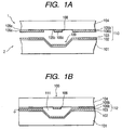
- Fig. 1A is a cross-sectional side view of a millimeter waveguide of the first embodiment in a condition before connection.
- Fig. 1B is a cross-sectional side view of the millimeter waveguide of the first embodiment in a connected condition.
- a millimeter waveguide 100 of the first embodiment comprises a single crystal substrate 101 having a groove 109 therein, a ground conductor film 110 on a surface of the groove 109 and a surface of the single crystal substrate 101 connecting to the surface of the groove 109, a single crystal substrate 104 covering the conductor film 110, and a microstrip line 108 on a surface of the single crystal substrate 108, exposed to a cavity 111 defined by the conductor film 110, the microstrip line 108, and the crystal substrate 104.
- the single crystal substrate 101 comprises a silicon substrate.
- the single crystal substrate 104 comprises a silicon substrate also.
- the ground conductor film 110 comprises: a conductor layer 102 on a surface of the crystal substrate 101 and a surface of the groove 109, a conductive connecting layer 112 on the conductor layer 102, a conductor film 105a on the conductive connecting layer 112 extending from an edge of the groove 109, and a conductor film 105b on the conductive connecting layer 112 extending from another edge of the groove 109.
- the conductor layers 102, 105a and 105b comprise nickel chromium.
- the microstrip line 108 comprises a foundation layer 105c on the surface of the second signal crystal substrate 104 and a conductive layer 106c on the foundation layer 105c.
- the foundation layer 105c comprises nickel chromium and the conductive layer 106c comprises gold.
- the conductive connecting layer 112 comprises gold.
- the groove 109 is formed in the single crystal substrate 101 made of a silicon by the anisotropic etching.
- the conductor layer 102 made of nickel chromium is formed on the surface of the single crystal substrate 101 and a surface of the groove 109.
- the conductive connecting layer 103 is formed on the conductor layer 102 with gold.
- the conductor layers 105a, 105b, 105c are formed on the surface of the single crystal substrate 104 with nickel chromium. Conductive connecting layers 106a and 106b are formed with gold. Then, both substrates 1 and 2 are connected by the thermo-compression bonding.
- This structure extends in the depth direction of the drawing as required.
- This structure provide a microstrip line with shielding.
- the shield structure can reduce a loss due to radiation in the millimeter band.
- Fig. 2 is a cross-sectional side view of a millimeter waveguide of the second embodiment.
- the millimeter waveguide of the second embodiment has substantially the same structure as that of the first embodiment. The difference is that a protruding portion 209 is formed on a bottom surface of the groove 219 at a middle of the bottom surface, extending along edges of the groove 219 in the depth direction of the drawing of Fig. 2.
- the conductor film 202 and the conductive connecting layer 203 cover a surface of the protruding portion 209.
- the current concentrates on both sides of the microstrip line 108.
- the current tends to flow through the middle portion of the microstrip line 108, so that a current density can be dispersed. Then, a loss in the microstrip line 108 can be further reduced.
- Fig. 3 is a cross-sectional side view of a millimeter waveguide of the third embodiment.
- the millimeter waveguide of the third embodiment comprises: a single crystal substrate 404, a conductor film 410 on a surface of the single crystal substrate 404, a single crystal substrate 401 on the conductor film 410, having a groove 409 on the side of the crystal substrate 404, and a microstrip line 408 on a bottom surface 409a of the groove 409.
- the difference from the first embodiment is that the microstrip line 408 is formed on the bottom surface of the groove 409 instead the crystal substrate 101. Therefore, the operation is similar to the first embodiment. However, the extent that the grounded conductor film surrounds the microstrip line is different between the first and third embodiments.
- Fig. 4A is a cross-sectional side view of a millimeter waveguide of the fourth embodiment in a condition before connection.
- Fig. 4B is a cross-sectional side view of the millimeter waveguide of the fourth embodiment in a connected condition.
- the millimeter waveguide of the third embodiment comprises a single crystal substrate 504 having a groove 509 therein, a conductor film 510 on a surface of the groove 509 and a surface of the single crystal substrate 504 connecting to the surface of the groove 509, a second crystal substrate 501 covering the conductor film 510 and the groove 509 and having a protrusion 511 toward the groove 509, and a microstrip line 508 on a surface of the protrusion 511, exposed to a cavity 513 defined by the conductor film 503 and the crystal substrate 501.
- a height H of the protrusion 511 is less than a depth D of the groove 509. In this embodiment, the height H is about a half of the depth D. Therefore, the protrusion 511 is formed such that the protrusion fits into the groove 509, wherein the cavity 513 is formed.
- the basic operation is similar to the first embodiment.
- the difference is that a shielding effect is higher than that of the first embodiment because the microstrip line 508 is surrounded by the conductor film 510, so that a loss due to radiation at millimeter band can be reduced.
- Fig. 5 is a cross-sectional side view of a circuit apparatus of the fourth embodiment using the structure of the millimeter waveguide 100 of the first embodiment.
- the crystal substrate 104' is processed to form a via hole 312 therein and then, microstrip lines 309 and 313 are formed in addition to forming the microstrip line 108 and the conductor films 105a to 105c and the conductive connecting films 106a and 106b as similar to the first embodiment. Then, the substrate 1' and 2 are connected by the thermo compression bonding. Then, the active circuit 310 is connected to the microstrip lines 309 and 313 with micro-bumps 311 by the flip chip bonding.
- the microstrip line 309 on the second single crystal substrate 104' is connected to the microstrip line 108 via the via hole 312.
- the active circuit chip 310 performs a predetermined circuit operation, such as an amplifying.
- the micro-bumps 111 mechanically and electrically connect the active circuit 310 to the microstrip line 313 and to the microstrip line 309.
- the microstrip line 313 is used for inputting an external signal to the active circuit or outputting a signal from the active circuit 310. Therefore, there is a responsive relation between the microstrip lines 108 and 313 through the active circuit 310, the via hole 312 and a microstrip line 309.
- the microstrip line 108 comprises the foundation layer 105c on the surface of the second signal crystal substrate 104' and the conductive layer 106c on the foundation layer 105c.
- the foundation layer 105c comprises nickel chromium and the conductive layer 106c comprises gold.
- Fig. 6 is a cross-sectional side view of a circuit apparatus of the sixth embodiment using the millimeter waveguide of the third embodiment.
- the structure of the sixth embodiment is similar to that of the fifth embodiment. The difference is that the structure of the millimeter waveguide of the third embodiment is used instead of that of the first embodiment.
- Fig. 7 is a cross-sectional side view of a circuit apparatus of the seventh embodiment using the millimeter waveguide of the fourth embodiment.
- the structure of the seventh embodiment is similar to that of the fifth embodiment. The difference is that the structure of the millimeter waveguide of the fourth embodiment is used instead of that of the first embodiment.
- Fig. 8A is a cross-sectional side view of a millimeter waveguide apparatus of the eighth embodiment.
- Fig. 8B is a plan view of the millimeter waveguide apparatus of the eighth embodiment.
- a millimeter waveguide of the eighth embodiment comprises a single crystal substrate 601 having a hollow portion 611 therein, a conductor film 612 on a surface of the hollow portion 611 and a surface of the single crystal substrate 601 connecting to the surface of the hollow portion 611, a conductor film 613 covering the hollow portion 611 and the conductor film 612, having a through hole 614 above the hollow portion 611, a single crystal substrate 604 on the conductor film 613, having a through hole 615 connected to the first hole 614, and a microstrip line 609 on a surface of the second single crystal substrate 604 opposite to the crystal substrate 601, and a probe 610 extending from the microstrip line 609 through the through holes 614 and 615, exposed to a cavity (611) defined by the conductor films 612 and 613.
- the probe 610 is connected to the microstrip line 609 as follows:
- the probe 610 has a dielectric substance 616 surrounding the probe 610. A tip of the dielectric substance 616 is stripped and is pierced through a through hole formed in the microstrip line 609. Then, the probe 610 is soldered.
- the microstrip line 609 comprises a foundation layer 609a on the surface of the second single crystal substrate 604 and a conductive layer 609b on the foundation layer.
- the foundation layer 609a comprises nickel chromium and the conductive layer 609b comprises gold.
- Fig. 9A is a cross-sectional side view of a millimeter waveguide apparatus of the ninth embodiment.
- Fig. 9B is a plan view of the millimeter waveguide apparatus of the ninth embodiment.
- a millimeter waveguide of the ninth embodiment has substantially similar to the eighth embodiment. The difference is that the through hole 615 is not formed and a slot 710 having a rectangular shape in the drawing of Fig. 9B instead the through hole 614.
- the microstrip line 709 is electromagnetically coupled to the cavity through the slot 710.
- This structure eliminates the necessity of fixing the probe 610 to the crystal.
Landscapes
- Waveguides (AREA)
- Micromachines (AREA)
- Drying Of Semiconductors (AREA)
- Control Of Motors That Do Not Use Commutators (AREA)
Claims (31)
- Millimeter-Hohlleiter (100), umfassend:wobei eines der Einkristallsubstrate (101; 201; 401; 504) eine Nut (109; 219; 409; 509) an einer dem anderen Substrat zugewandten Oberfläche aufweist; underste und zweite Einkristallsubstrate (101, 104; 201, 104; 404, 401; 504, 501), die übereinander angeordnet sind;
einen Leiterfilm (110; 410; 510), der auf Masse zu legen ist, auf einer Oberfläche des ersten Einkristallsubstrates (101; 201; 404; 504);
wobei das zweite Einkristallsubstrat (104; 401; 501) den Leiterfilm (110; 410; 510) bedeckt,
gekennzeichnet durch
eine Mikrostreifenleitung (108; 408; 508) auf einer Oberfläche des zweiten Einkristallsubstrates (104; 401; 501), die zu einem Hohlraum (111; 513) hin frei liegt, der durch die Nut (109; 219; 409; 509) ausgebildet und zwischen dem Leiterfilm (110; 410; 510) und dem zweiten Einkristallsubstrat (104; 401; 501) definiert ist. - Millimeter-Hohlleiter nach Anspruch 1, wobei das erste Einkristallsubstrat (101) die Nut (109) aufweist.
- Millimeter-Hohlleiter nach Anspruch 2, wobei das erste und/oder das zweite Einkristallsubstrat (101, 104) ein Siliziumsubstrat umfassen.
- Millimeter-Hohlleiter nach Anspruch 2, wobei der Leiterfilm (110) umfasst:eine erste Leiterschicht (102) auf dem ersten Kristallsubstrat (101), die die Nut (109) bedeckt;eine leitende Verbindungsschicht (112) auf der ersten Leiterschicht (102);einen zweiten Leiterfilm (105a) auf der leitenden Verbindungsschicht (112), der sich von einer Kante der Nut (109) aus erstreckt; undeinen dritten Leiterfilm (105b) auf der leitenden Verbindungsschicht (112), der sich von einer anderen Kante der Nut (109) aus erstreckt.
- Millimeter-Hohlleiter nach Anspruch 2, wobei die erste und die zweite leitende Schicht (102, 105a) Nickel-Chrom umfassen.
- Millimeter-Hohlleiter nach Anspruch 2 oder Anspruch 5, wobei die leitende Verbindungsschicht (112) Gold umfasst.
- Millimeter-Hohlleiter nach Anspruch 2, wobei das erste Einkristallsubstrat (201) ferner einen vorspringenden Abschnitt (209) an einer Bodenfläche der Nut (219) in einer Mitte der Bodenfläche umfasst, der sich entlang der Nut (219) erstreckt, so dass er der Mikrostreifenleitung (108) gegenüber liegt, wobei der erste leitende Film (203) eine Oberfläche des vorspringenden Abschnittes (209) bedeckt.
- Millimeter-Hohlleiter nach Anspruch 2, wobei das zweite Einkristallsubstrat (104) ein Durchgangsloch (312) aufweist, wobei der Millimeter-Hohlleiter ferner eine zweite Mikrostreifenleitung (309) auf einer entgegengesetzten Oberfläche des zweiten Einkristallsubstrates (104) umfasst, die mit der Mikrostreifenleitung (108) über das Durchgangsloch (312) zur Kopplung der Mikrostreifenleitung (108) mit einer externen Schaltung (310) verbunden ist.
- Millimeter-Hohlleiter nach Anspruch 1, wobei
das zweite Einkristallsubstrat (401) die Nut auf der Seite des ersten Kristallsubstrats (404) aufweist; und
wobei die Mikrostreifenleitung (408) auf einer Bodenfläche der Nut (409) angeordnet ist. - Millimeter-Hohlleiter nach Anspruch 9, wobei das erste Einkristallsubstrat (404) ein Siliziumsubstrat umfasst.
- Millimeter-Hohlleiter nach Anspruch 9, wobei das zweite Einkristallsubstrat (401) ein Siliziumsubstrat umfasst.
- Millimeter-Hohlleiter nach Anspruch 9, wobei der Leiterfilm (410) umfasst:eine erste Leiterschicht auf dem ersten Kristallsubstrat (404);eine leitende Verbindungsschicht auf der ersten Leiterschicht; undeinen zweiten Leiterfilm auf der leitenden Verbindungsschicht, der sich von einer Kante der Nut (409) aus erstreckt; undeinen dritten Leiterfilm auf der leitenden Verbindungsschicht, der sich von einer anderen Kante der Nut (409) aus erstreckt.
- Millimeter-Hohlleiter nach Anspruch 12, wobei die erste und die zweite Leiterschicht Nickel-Chrom umfassen.
- Millimeter-Hohlleiter nach Anspruch 12, wobei die leitende Verbindungsschicht Gold umfasst.
- Millimeter-Hohlleiter nach einem der Ansprüche 1 bis 6, wobei
das zweite Einkristallsubstrat (501) einen Vorsprung (511) in Richtung der Nut (509) aufweist; und
die Mikrostreifenleitung (508) auf einer Oberfläche des Vorsprunges (511) gebildet ist und zu dem Hohlraum (513) frei liegt,
wobei eine Höhe des Vorsprunges (511) geringer als eine Tiefe der Nut (509) ist. - Millimeter-Hohlleiter, umfassend:gekennzeichnet durchein erstes Einkristallsubstrat (601) mit einem hohlen Abschnitt (611) darin; undeinen ersten Leiterfilm (612), der auf Masse zu legen ist, auf einer Oberfläche des hohlen Abschnittes (611) und einer Oberfläche des ersten Einkristallsubstrates (601), die mit der Oberfläche des hohlen Abschnittes (611) verbunden ist;
einen zweiten Leiterfilm (613; 713), der den hohlen Abschnitt (611) und die Oberfläche des ersten Einkristallsubstrats (601) bedeckt und ein Durchtrittsloch (614) oder einen Durchgangsschlitz (710) über dem hohlen Abschnitt aufweist;
ein zweites Einkristallsubstrat (604; 704) auf dem zweiten Leiterfilm (613; 713);
einen Hohlraum (611), der durch den ersten und den zweiten Leiterfilm (612, 613; 713) definiert ist; und
eine Mikrostreifenleitung (609; 709) auf einer Oberfläche des zweiten Einkristallsubstrates (604; 704) entgegengesetzt zu dem ersten Einkristallsubstrat (601), um eine elektromagnetische Kopplung mit dem Hohlraum (611) durch das Durchtrittsloch (614) oder den Durchgangsschlitz (710) und das zweite Einkristallsubstrat (604; 704) herzustellen. - Millimeter-Hohlleiter nach Anspruch 16, wobei
das zweite Einkristallsubstrat (604) ein zweites Durchtrittsloch (615) aufweist, das mit dem ersten Loch (614) verbunden ist; und
eine Sonde (610) sich von der Mikrostreifenleitung (609) durch das erste und das zweite Durchtrittsloch erstreckt und zu dem Hohlraum (611) frei liegt. - Schaltungsvorrichtung, umfassend:einen Millimeter-Hohlleiter nach Anspruch 8;eine dritte Mikrostreifenleitung (313) auf der entgegengesetzten Oberfläche getrennt von der zweiten Mikrostreifenleitung (309);einen aktiven Schaltungs-Chip (310) zum Durchführen eines vorbestimmten Schaltvorganges; undein Verbindungsmittel zum mechanischen und elektrischen Verbinden der aktiven Schaltung (310) mit der dritten Mikrostreifenleitung (313) und mit der zweiten Mikrostreifenleitung (309), wobei es eine Ansprechbeziehung zwischen der ersten und der dritten Mikrostreifenleitung (108, 313) durch die aktive Schaltung (310), die zweite Mikrostreifenleitung (309) und das Durchgangsloch (312) gibt.
- Schaltungsvorrichtung, umfassend:einen Millimeter-Hohlleiter nach Anspruch 9;eine zweite Mikrostreifenleitung (309) auf einer Oberfläche des zweiten Einkristallsubstrates (401) entgegengesetzt zu der Nut, die mit der ersten Mikrostreifenleitung (408) über ein Durchgangsloch (312) verbunden ist; undeine dritte Mikrostreifenleitung (313) auf der Oberfläche des zweiten Einkristallsubstrates (401) getrennt von der zweiten Mikrostreifenleitung (309);einen aktiven Schaltungs-Chip (310) zum Durchführen eines vorbestimmten Schaltvorganges; undein Verbindungsmittel zum mechanischen und elektrischen Verbinden der aktiven Schaltung (310) mit der dritten Mikrostreifenleitung (313) und mit der zweiten Mikrostreifenleitung (309), wobei es eine Ansprechbeziehung zwischen der ersten und der dritten Mikrostreifenleitung (408, 313) durch die aktive Schaltung (310), die zweite Mikrostreifenleitung (309) und das Durchgangsloch (312) gibt.
- Schaltungsvorrichtung, umfassend:wobei es eine Ansprechbeziehung zwischen der ersten und der dritten Mikrostreifenleitung (508, 313) durch die aktive Schaltung (310), die zweite Mikrostreifenleitung (309) und das Durchgangsloch (312) gibt.einen Millimeter-Hohlleiter nach Anspruch 15;eine zweite Mikrostreifenleitung (309) auf einer Oberfläche des zweiten Einkristallsubstrates (501) entgegengesetzt zu dem Vorsprung, die mit der ersten Mikrostreifenleitung (508) über ein Durchgangsloch (312) verbunden ist; undeine dritte Mikrostreifenleitung auf der Oberfläche des zweiten Einkristallsubstrates (501) getrennt von der zweiten Mikrostreifenleitung (309); undeinen aktiven Schaltungs-Chip (310) zum Durchführen eines vorbestimmten Schaltvorganges; undein Verbindungsmittel (311) zum mechanischen und elektrischen Verbinden der aktiven Schaltung (310) mit der dritten Mikrostreifenleitung (313) und mit der zweiten Mikrostreifenleitung (309),
- Millimeter-Hohlleiter nach Anspruch 15, wobei die erste und die zweite leitende Schicht Nickel-Chrom umfassen, und die leitende Verbindungsschicht Gold umfasst.
- Schaltungsvorrichtung nach Anspruch 18, wobei das Verbindungsmittel Mikro-Anschlusshöcker umfasst.
- Millimeter-Hohlleiter nach Anspruch 2, wobei die Mikrostreifenleitung (108) eine Grundschicht auf der Oberfläche des zweiten Einkristallsubstrats (104) und eine leitende Schicht auf der Grundschicht umfasst.
- Millimeter-Hohlleiter nach Anspruch 9,
wobei die Mikrostreifenleitung (408) eine Grundschicht auf der Bodenfläche der Nut (409) und eine leitende Schicht auf der Grundschicht umfasst. - Millimeter-Hohlleiter nach Anspruch 15,
wobei die Mikrostreifenleitung (508) eine Grundschicht auf der Oberfläche des Vorsprungs (511) und eine leitende Schicht auf der Grundschicht umfasst. - Millimeter-Hohlleiter nach Anspruch 17,
wobei die Mikrostreifenleitung eine Grundschicht auf der Oberfläche des zweiten Einkristallsubstrates und eine leitende Schicht auf der Grundschicht umfasst. - Millimeter-Hohlleiter nach Anspruch 16,
wobei die Mikrostreifenleitung (609) eine Grundschicht auf der Oberfläche des zweiten Einkristallsubstrates (604) und eine leitende Schicht auf der Grundschicht umfasst. - Schaltungsvorrichtung nach Anspruch 18,
wobei die erste Mikrostreifenleitung eine Grundschicht auf der Oberfläche des zweiten Einkristallsubstrates und eine leitende Schicht auf der Grundschicht umfasst. - Schaltungsvorrichtung nach Anspruch 19,
wobei die erste Mikrostreifenleitung eine Grundschicht auf der Bodenfläche der Nut und eine leitende Schicht auf der Grundschicht umfasst. - Schaltungsvorrichtung nach Anspruch 20,
wobei die erste Mikrostreifenleitung eine Grundschicht auf der Oberfläche des Vorsprunges und eine leitende Schicht auf der Grundschicht umfasst. - Schaltungsvorrichtung nach einem der Ansprüche 23 bis 30,
wobei die Grundschicht Nickel-Chrom und die leitende Schicht Gold umfasst.
Applications Claiming Priority (3)
| Application Number | Priority Date | Filing Date | Title |
|---|---|---|---|
| JP31736296A JP3218996B2 (ja) | 1996-11-28 | 1996-11-28 | ミリ波導波路 |
| JP317362/96 | 1996-11-28 | ||
| JP31736296 | 1996-11-28 |
Publications (3)
| Publication Number | Publication Date |
|---|---|
| EP0845831A2 EP0845831A2 (de) | 1998-06-03 |
| EP0845831A3 EP0845831A3 (de) | 1999-03-10 |
| EP0845831B1 true EP0845831B1 (de) | 2005-04-27 |
Family
ID=18087402
Family Applications (1)
| Application Number | Title | Priority Date | Filing Date |
|---|---|---|---|
| EP97120769A Expired - Lifetime EP0845831B1 (de) | 1996-11-28 | 1997-11-26 | Millimeter-Hohlleiter und Schaltungsanordnung mit diesem Hohlleiter |
Country Status (4)
| Country | Link |
|---|---|
| US (1) | US5990768A (de) |
| EP (1) | EP0845831B1 (de) |
| JP (1) | JP3218996B2 (de) |
| DE (1) | DE69733115T2 (de) |
Cited By (5)
| Publication number | Priority date | Publication date | Assignee | Title |
|---|---|---|---|---|
| US8866300B1 (en) | 2011-06-05 | 2014-10-21 | Nuvotronics, Llc | Devices and methods for solder flow control in three-dimensional microstructures |
| US8917150B2 (en) | 2010-01-22 | 2014-12-23 | Nuvotronics, Llc | Waveguide balun having waveguide structures disposed over a ground plane and having probes located in channels |
| US8933769B2 (en) | 2006-12-30 | 2015-01-13 | Nuvotronics, Llc | Three-dimensional microstructures having a re-entrant shape aperture and methods of formation |
| US9000863B2 (en) | 2007-03-20 | 2015-04-07 | Nuvotronics, Llc. | Coaxial transmission line microstructure with a portion of increased transverse dimension and method of formation thereof |
| US9024417B2 (en) | 2007-03-20 | 2015-05-05 | Nuvotronics, Llc | Integrated electronic components and methods of formation thereof |
Families Citing this family (62)
| Publication number | Priority date | Publication date | Assignee | Title |
|---|---|---|---|---|
| US6549105B2 (en) | 1998-06-02 | 2003-04-15 | Matsushita Electric Industrial Co., Ltd. | Millimeter wave module and radio apparatus |
| US6778041B2 (en) * | 1998-06-02 | 2004-08-17 | Matsushita Electric Industrial Co., Ltd. | Millimeter wave module and radio apparatus |
| JP3331967B2 (ja) | 1998-06-02 | 2002-10-07 | 松下電器産業株式会社 | ミリ波モジュール |
| US6483406B1 (en) * | 1998-07-31 | 2002-11-19 | Kyocera Corporation | High-frequency module using slot coupling |
| KR100308871B1 (ko) * | 1998-12-28 | 2001-11-03 | 윤덕용 | 동축 구조의 신호선 및 그의 제조 방법 |
| JP3282608B2 (ja) * | 1999-03-23 | 2002-05-20 | 日本電気株式会社 | 多層基板 |
| FI113580B (fi) * | 1999-03-31 | 2004-05-14 | Nokia Corp | Invertoitu mikroliuska-siirtolinja monikerrosrakenteeseen integroituna |
| KR100513709B1 (ko) * | 1999-03-31 | 2005-09-07 | 삼성전자주식회사 | 전압제어발진기의 위상 잡음 감소용 공동공진기 및 그 제작방법 |
| KR20010077106A (ko) * | 2000-01-31 | 2001-08-17 | 김용권 | 코플래나 웨이브 가이드 |
| KR100379440B1 (ko) * | 2000-02-16 | 2003-04-10 | 엘지전자 주식회사 | 마이크로웨이브 공진기 제조방법 |
| USRE44438E1 (en) | 2001-02-27 | 2013-08-13 | Stats Chippac, Ltd. | Semiconductor device and method of dissipating heat from thin package-on-package mounted to substrate |
| US20020121707A1 (en) * | 2001-02-27 | 2002-09-05 | Chippac, Inc. | Super-thin high speed flip chip package |
| US8143108B2 (en) | 2004-10-07 | 2012-03-27 | Stats Chippac, Ltd. | Semiconductor device and method of dissipating heat from thin package-on-package mounted to substrate |
| US6512431B2 (en) | 2001-02-28 | 2003-01-28 | Lockheed Martin Corporation | Millimeterwave module compact interconnect |
| KR100382765B1 (ko) * | 2001-06-15 | 2003-05-09 | 삼성전자주식회사 | 송수신용 수동소자와 그 집적모듈 및 그 제조방법 |
| US6882762B2 (en) * | 2001-09-27 | 2005-04-19 | Intel Corporation | Waveguide in a printed circuit board and method of forming the same |
| JP4159378B2 (ja) | 2002-04-25 | 2008-10-01 | 三菱電機株式会社 | 高周波装置とその製造方法 |
| JP2004207625A (ja) * | 2002-12-26 | 2004-07-22 | Sony Corp | 多層構造体およびその製造方法ならびに機能構造体およびその製造方法ならびに電子線露光用マスクおよびその製造方法 |
| DE10304835A1 (de) * | 2003-02-06 | 2004-08-05 | Robert Bosch Gmbh | Mikroelektromechanisches Bauelement |
| ATE475999T1 (de) * | 2003-03-04 | 2010-08-15 | Rohm & Haas Elect Mat | Koaxiale wellenleitermikrostrukturen und verfahern zu ihrer bildung |
| KR100538470B1 (ko) * | 2003-09-15 | 2005-12-23 | 한국과학기술원 | 유전체 박막을 이용한 동축선 구조의 전송선 시스템, 그제조 방법 및 그를 이용한 패키지 방법 |
| US7298234B2 (en) * | 2003-11-25 | 2007-11-20 | Banpil Photonics, Inc. | High speed electrical interconnects and method of manufacturing |
| CN1293667C (zh) * | 2003-12-19 | 2007-01-03 | 上海交通大学 | 基于微机电系统的倒置微带传输线及其制造方法 |
| DE102004022177B4 (de) * | 2004-05-05 | 2008-06-19 | Atmel Germany Gmbh | Verfahren zur Herstellung eines Koplanarleitungssystem auf einem Substrat und nach einem derartigen Verfahren hergestelltes Bauelement zur Übertragung von elektromagnetischen Wellen |
| DE102004022178B4 (de) * | 2004-05-05 | 2008-03-20 | Atmel Germany Gmbh | Verfahren zur Herstellung einer Leiterbahn auf einem Substrat und Bauelement mit einer derart hergestellten Leiterbahn |
| JP2006222609A (ja) * | 2005-02-09 | 2006-08-24 | Sony Corp | 高周波信号伝送回路の製造方法及び高周波信号伝送回路装置 |
| JP4823541B2 (ja) * | 2005-03-18 | 2011-11-24 | 富士通セミコンダクター株式会社 | 高周波伝送線路 |
| FR2885735B1 (fr) | 2005-05-10 | 2007-08-03 | St Microelectronics Sa | Circuit integre guide d'ondes |
| FI20055511A7 (fi) * | 2005-09-27 | 2007-03-28 | Filtronic Comtek Oy | Siirtojohtorakenne |
| JP2008188754A (ja) | 2006-12-30 | 2008-08-21 | Rohm & Haas Electronic Materials Llc | 三次元微細構造体およびその形成方法 |
| US8324728B2 (en) * | 2007-11-30 | 2012-12-04 | Skyworks Solutions, Inc. | Wafer level packaging using flip chip mounting |
| EP2343774A4 (de) * | 2008-10-29 | 2013-11-27 | Panasonic Corp | Hochfrequenzwellenleiter und phasenverschieber damit, heizkörper, elektronische vorrichtung mit besagtem phasenverschieber und dem heizkörper, antennenvorrichtung sowie elektronische vorrichtung damit |
| US8659371B2 (en) * | 2009-03-03 | 2014-02-25 | Bae Systems Information And Electronic Systems Integration Inc. | Three-dimensional matrix structure for defining a coaxial transmission line channel |
| US20110123783A1 (en) | 2009-11-23 | 2011-05-26 | David Sherrer | Multilayer build processses and devices thereof |
| KR101917052B1 (ko) | 2010-01-22 | 2019-01-30 | 누보트로닉스, 인크. | 열관리 |
| FR2976120A1 (fr) | 2011-06-01 | 2012-12-07 | St Microelectronics Sa | Procede de fabrication d'un circuit integre comprenant au moins un guide d'ondes coplanaire |
| US8814601B1 (en) | 2011-06-06 | 2014-08-26 | Nuvotronics, Llc | Batch fabricated microconnectors |
| JP6335782B2 (ja) | 2011-07-13 | 2018-05-30 | ヌボトロニクス、インク. | 電子的および機械的な構造を製作する方法 |
| CN102513393A (zh) * | 2011-12-23 | 2012-06-27 | 成都泰格微波技术股份有限公司 | 微小型毫米波波导器件的制造方法 |
| US9325044B2 (en) | 2013-01-26 | 2016-04-26 | Nuvotronics, Inc. | Multi-layer digital elliptic filter and method |
| US9306255B1 (en) | 2013-03-15 | 2016-04-05 | Nuvotronics, Inc. | Microstructure including microstructural waveguide elements and/or IC chips that are mechanically interconnected to each other |
| US9306254B1 (en) | 2013-03-15 | 2016-04-05 | Nuvotronics, Inc. | Substrate-free mechanical interconnection of electronic sub-systems using a spring configuration |
| US9219298B2 (en) | 2013-03-15 | 2015-12-22 | International Business Machines Corporation | Removal of spurious microwave modes via flip-chip crossover |
| US9520547B2 (en) | 2013-03-15 | 2016-12-13 | International Business Machines Corporation | Chip mode isolation and cross-talk reduction through buried metal layers and through-vias |
| WO2015109208A2 (en) | 2014-01-17 | 2015-07-23 | Nuvotronics, Llc | Wafer scale test interface unit: low loss and high isolation devices and methods for high speed and high density mixed signal interconnects and contactors |
| CN104377415A (zh) * | 2014-10-08 | 2015-02-25 | 石以瑄 | 用于微波传输的共面波导及其制作方法 |
| US10847469B2 (en) | 2016-04-26 | 2020-11-24 | Cubic Corporation | CTE compensation for wafer-level and chip-scale packages and assemblies |
| US10511073B2 (en) | 2014-12-03 | 2019-12-17 | Cubic Corporation | Systems and methods for manufacturing stacked circuits and transmission lines |
| US9941560B2 (en) * | 2014-12-22 | 2018-04-10 | The Regents Of The University Of Michigan | Non-contact on-wafer S-parameter measurements of devices at millimeter-wave to terahertz frequencies |
| WO2016120254A1 (en) * | 2015-01-27 | 2016-08-04 | At & S Austria Technologie & Systemtechnik Aktiengesellschaft | Component carrier with integrated antenna structure |
| US10068181B1 (en) | 2015-04-27 | 2018-09-04 | Rigetti & Co, Inc. | Microwave integrated quantum circuits with cap wafer and methods for making the same |
| CN208608339U (zh) * | 2016-01-27 | 2019-03-15 | 株式会社村田制作所 | 信号传输线路 |
| EP3449532B1 (de) | 2016-04-28 | 2024-02-28 | AT & S Austria Technologie & Systemtechnik Aktiengesellschaft | Komponententräger mit integrierter antennenanordnung, elektronische vorrichtung, funkkommunikationsverfahren |
| WO2018038707A1 (en) * | 2016-08-23 | 2018-03-01 | Intel Corporation | Inverted microstrip transmission lines for qubits |
| US11276727B1 (en) | 2017-06-19 | 2022-03-15 | Rigetti & Co, Llc | Superconducting vias for routing electrical signals through substrates and their methods of manufacture |
| US11121301B1 (en) | 2017-06-19 | 2021-09-14 | Rigetti & Co, Inc. | Microwave integrated quantum circuits with cap wafers and their methods of manufacture |
| US11527696B2 (en) * | 2017-10-05 | 2022-12-13 | Google Llc | Low footprint resonator in flip chip geometry |
| US10319654B1 (en) | 2017-12-01 | 2019-06-11 | Cubic Corporation | Integrated chip scale packages |
| CN108601204A (zh) * | 2018-05-25 | 2018-09-28 | 上海安费诺永亿通讯电子有限公司 | 一种低损耗扁平传输线 |
| US10998638B2 (en) | 2019-01-31 | 2021-05-04 | Toyota Motor Engineering & Manufacturing North America, Inc. | Nickel-chromium particles and multilayer structures comprising nickel chromium core layers |
| US11963911B2 (en) | 2020-02-13 | 2024-04-23 | Bone Foam, Inc. | Anterior cervical positioning system |
| US11339495B2 (en) | 2020-05-20 | 2022-05-24 | Toyota Motor Engineering & Manufacturing North America, Inc. | Coated discrete metallic particles and multilayer structures comprising reflective core layers |
Family Cites Families (7)
| Publication number | Priority date | Publication date | Assignee | Title |
|---|---|---|---|---|
| US5012319A (en) * | 1990-05-14 | 1991-04-30 | At&T Bell Laboratories | Integrated electronic assembly comprising a transmission line |
| JPH04115604A (ja) * | 1990-08-31 | 1992-04-16 | Matsushita Electric Ind Co Ltd | マイクロ波回路 |
| US5138436A (en) * | 1990-11-16 | 1992-08-11 | Ball Corporation | Interconnect package having means for waveguide transmission of rf signals |
| US5303419A (en) * | 1992-05-29 | 1994-04-12 | Her Majesty The Queen In Right Of Canada As Represented By The Minister Of Communications | Aperture-coupled line Magic-Tee and mixer formed therefrom |
| JP3161068B2 (ja) * | 1992-08-28 | 2001-04-25 | 日産自動車株式会社 | 半導体ミリ波装置 |
| US5471181A (en) * | 1994-03-08 | 1995-11-28 | Hughes Missile Systems Company | Interconnection between layers of striplines or microstrip through cavity backed slot |
| FR2738395B1 (fr) * | 1995-08-31 | 1997-10-10 | Commissariat Energie Atomique | Dispositif autoporte pour la propagation d'ondes hyperfrequences et procedes de realisation d'un tel dispositif |
-
1996
- 1996-11-28 JP JP31736296A patent/JP3218996B2/ja not_active Expired - Fee Related
-
1997
- 1997-11-26 DE DE69733115T patent/DE69733115T2/de not_active Expired - Fee Related
- 1997-11-26 US US08/978,617 patent/US5990768A/en not_active Expired - Lifetime
- 1997-11-26 EP EP97120769A patent/EP0845831B1/de not_active Expired - Lifetime
Cited By (5)
| Publication number | Priority date | Publication date | Assignee | Title |
|---|---|---|---|---|
| US8933769B2 (en) | 2006-12-30 | 2015-01-13 | Nuvotronics, Llc | Three-dimensional microstructures having a re-entrant shape aperture and methods of formation |
| US9000863B2 (en) | 2007-03-20 | 2015-04-07 | Nuvotronics, Llc. | Coaxial transmission line microstructure with a portion of increased transverse dimension and method of formation thereof |
| US9024417B2 (en) | 2007-03-20 | 2015-05-05 | Nuvotronics, Llc | Integrated electronic components and methods of formation thereof |
| US8917150B2 (en) | 2010-01-22 | 2014-12-23 | Nuvotronics, Llc | Waveguide balun having waveguide structures disposed over a ground plane and having probes located in channels |
| US8866300B1 (en) | 2011-06-05 | 2014-10-21 | Nuvotronics, Llc | Devices and methods for solder flow control in three-dimensional microstructures |
Also Published As
| Publication number | Publication date |
|---|---|
| EP0845831A2 (de) | 1998-06-03 |
| EP0845831A3 (de) | 1999-03-10 |
| JP3218996B2 (ja) | 2001-10-15 |
| DE69733115T2 (de) | 2006-03-02 |
| DE69733115D1 (de) | 2005-06-02 |
| JPH10163711A (ja) | 1998-06-19 |
| US5990768A (en) | 1999-11-23 |
Similar Documents
| Publication | Publication Date | Title |
|---|---|---|
| EP0845831B1 (de) | Millimeter-Hohlleiter und Schaltungsanordnung mit diesem Hohlleiter | |
| US6040739A (en) | Waveguide to microstrip backshort with external spring compression | |
| JP3500268B2 (ja) | 高周波用入出力端子ならびにそれを用いた高周波用半導体素子収納用パッケージ | |
| US6958662B1 (en) | Waveguide to stripline transition with via forming an impedance matching fence | |
| US6362706B1 (en) | Cavity resonator for reducing phase noise of voltage controlled oscillator | |
| US6674347B1 (en) | Multi-layer substrate suppressing an unwanted transmission mode | |
| US20030076188A1 (en) | Transmission line to waveguide transition structures | |
| US8234777B2 (en) | Low profile and compact surface mount circulator on ball grid array | |
| CA2312128A1 (en) | Mmic-to-waveguide rf transition and associated method | |
| US6255730B1 (en) | Integrated low cost thick film RF module | |
| US5629654A (en) | Coplanar waveguide coupler | |
| AU676114B2 (en) | End launched microstrip (or stripline)to waveguide transition using a cavity backed slot fed by a t-shaped microstrip line | |
| JP5728101B1 (ja) | Mmic集積回路モジュール | |
| JP4646969B2 (ja) | 半導体装置 | |
| JP3303226B2 (ja) | フリップチップ実装構造 | |
| JPH07202520A (ja) | マイクロ波回路 | |
| KR102904358B1 (ko) | 레이더 센서들을 위한 고주파 어셈블리 | |
| JP2803551B2 (ja) | マイクロストリップ導波管変換回路 | |
| JP3409767B2 (ja) | 高周波回路基板 | |
| JP4055028B2 (ja) | 金属ベース配線板とその製造方法 | |
| JPH05199019A (ja) | 高周波回路パッケージ | |
| JPH04276905A (ja) | ストリップ線路の製造方法 | |
| JP2002057513A (ja) | ミリ波モジュール | |
| JP2791301B2 (ja) | マイクロ波集積回路及びマイクロ波回路装置 | |
| JP2002050733A (ja) | 高周波用パッケージ、配線ボードおよび高周波モジュール |
Legal Events
| Date | Code | Title | Description |
|---|---|---|---|
| PUAI | Public reference made under article 153(3) epc to a published international application that has entered the european phase |
Free format text: ORIGINAL CODE: 0009012 |
|
| 17P | Request for examination filed |
Effective date: 19971126 |
|
| AK | Designated contracting states |
Kind code of ref document: A2 Designated state(s): DE GB |
|
| AX | Request for extension of the european patent |
Free format text: AL;LT;LV;MK;RO;SI |
|
| PUAL | Search report despatched |
Free format text: ORIGINAL CODE: 0009013 |
|
| AK | Designated contracting states |
Kind code of ref document: A3 Designated state(s): AT BE CH DE DK ES FI FR GB GR IE IT LI LU MC NL PT SE |
|
| AX | Request for extension of the european patent |
Free format text: AL;LT;LV;MK;RO;SI |
|
| AKX | Designation fees paid |
Free format text: DE GB |
|
| 17Q | First examination report despatched |
Effective date: 20020301 |
|
| GRAP | Despatch of communication of intention to grant a patent |
Free format text: ORIGINAL CODE: EPIDOSNIGR1 |
|
| GRAS | Grant fee paid |
Free format text: ORIGINAL CODE: EPIDOSNIGR3 |
|
| GRAA | (expected) grant |
Free format text: ORIGINAL CODE: 0009210 |
|
| AK | Designated contracting states |
Kind code of ref document: B1 Designated state(s): DE GB |
|
| REG | Reference to a national code |
Ref country code: GB Ref legal event code: FG4D |
|
| REF | Corresponds to: |
Ref document number: 69733115 Country of ref document: DE Date of ref document: 20050602 Kind code of ref document: P |
|
| PLBE | No opposition filed within time limit |
Free format text: ORIGINAL CODE: 0009261 |
|
| STAA | Information on the status of an ep patent application or granted ep patent |
Free format text: STATUS: NO OPPOSITION FILED WITHIN TIME LIMIT |
|
| 26N | No opposition filed |
Effective date: 20060130 |
|
| PGFP | Annual fee paid to national office [announced via postgrant information from national office to epo] |
Ref country code: GB Payment date: 20061122 Year of fee payment: 10 |
|
| PGFP | Annual fee paid to national office [announced via postgrant information from national office to epo] |
Ref country code: DE Payment date: 20061123 Year of fee payment: 10 |
|
| GBPC | Gb: european patent ceased through non-payment of renewal fee |
Effective date: 20071126 |
|
| PG25 | Lapsed in a contracting state [announced via postgrant information from national office to epo] |
Ref country code: DE Free format text: LAPSE BECAUSE OF NON-PAYMENT OF DUE FEES Effective date: 20080603 |
|
| PG25 | Lapsed in a contracting state [announced via postgrant information from national office to epo] |
Ref country code: GB Free format text: LAPSE BECAUSE OF NON-PAYMENT OF DUE FEES Effective date: 20071126 |