EP0833340A1 - Leseschaltung für Halbleiter-Speicherzellen - Google Patents
Leseschaltung für Halbleiter-Speicherzellen Download PDFInfo
- Publication number
- EP0833340A1 EP0833340A1 EP96830494A EP96830494A EP0833340A1 EP 0833340 A1 EP0833340 A1 EP 0833340A1 EP 96830494 A EP96830494 A EP 96830494A EP 96830494 A EP96830494 A EP 96830494A EP 0833340 A1 EP0833340 A1 EP 0833340A1
- Authority
- EP
- European Patent Office
- Prior art keywords
- circuit
- cell
- read circuit
- memory cells
- elements
- Prior art date
- Legal status (The legal status is an assumption and is not a legal conclusion. Google has not performed a legal analysis and makes no representation as to the accuracy of the status listed.)
- Granted
Links
- 239000004065 semiconductor Substances 0.000 title claims abstract description 6
- 230000015654 memory Effects 0.000 claims description 27
- 239000003990 capacitor Substances 0.000 claims description 24
- 238000003860 storage Methods 0.000 claims description 5
- 230000005540 biological transmission Effects 0.000 claims 1
- 238000000034 method Methods 0.000 description 24
- XUIMIQQOPSSXEZ-UHFFFAOYSA-N Silicon Chemical compound [Si] XUIMIQQOPSSXEZ-UHFFFAOYSA-N 0.000 description 2
- 238000010586 diagram Methods 0.000 description 2
- 238000007599 discharging Methods 0.000 description 2
- 230000010354 integration Effects 0.000 description 2
- 229910052710 silicon Inorganic materials 0.000 description 2
- 239000010703 silicon Substances 0.000 description 2
- 230000003321 amplification Effects 0.000 description 1
- 230000002401 inhibitory effect Effects 0.000 description 1
- 238000004519 manufacturing process Methods 0.000 description 1
- 238000003199 nucleic acid amplification method Methods 0.000 description 1
- 230000002093 peripheral effect Effects 0.000 description 1
- 238000003825 pressing Methods 0.000 description 1
- 230000000630 rising effect Effects 0.000 description 1
- 230000035945 sensitivity Effects 0.000 description 1
- 238000006467 substitution reaction Methods 0.000 description 1
- 230000001052 transient effect Effects 0.000 description 1
Images

Classifications
-
- G—PHYSICS
- G11—INFORMATION STORAGE
- G11C—STATIC STORES
- G11C7/00—Arrangements for writing information into, or reading information out from, a digital store
- G11C7/06—Sense amplifiers; Associated circuits, e.g. timing or triggering circuits
- G11C7/062—Differential amplifiers of non-latching type, e.g. comparators, long-tailed pairs
-
- G—PHYSICS
- G11—INFORMATION STORAGE
- G11C—STATIC STORES
- G11C11/00—Digital stores characterised by the use of particular electric or magnetic storage elements; Storage elements therefor
- G11C11/56—Digital stores characterised by the use of particular electric or magnetic storage elements; Storage elements therefor using storage elements with more than two stable states represented by steps, e.g. of voltage, current, phase, frequency
- G11C11/5621—Digital stores characterised by the use of particular electric or magnetic storage elements; Storage elements therefor using storage elements with more than two stable states represented by steps, e.g. of voltage, current, phase, frequency using charge storage in a floating gate
- G11C11/5642—Sensing or reading circuits; Data output circuits
-
- G—PHYSICS
- G11—INFORMATION STORAGE
- G11C—STATIC STORES
- G11C7/00—Arrangements for writing information into, or reading information out from, a digital store
- G11C7/06—Sense amplifiers; Associated circuits, e.g. timing or triggering circuits
- G11C7/065—Differential amplifiers of latching type
-
- G—PHYSICS
- G11—INFORMATION STORAGE
- G11C—STATIC STORES
- G11C7/00—Arrangements for writing information into, or reading information out from, a digital store
- G11C7/06—Sense amplifiers; Associated circuits, e.g. timing or triggering circuits
Definitions
- This invention relates to circuits contained in and integrated to memory cell devices, and particularly to a circuit for reading memory cells by a technique which utilizes reference cells.
- a pressing problem is to provide circuitry that can give access to stored information in less time, and requires less power to do so, while ensuring highly reliable reading of the stored data, to thereby fill the market's demands.
- Reading by reference cells involves the use of a non-volatile memory cell identical with the memory cell being selected by the decode blocks; regardless of whether the selected cell is written or not (i.e., has a high or low threshold), the reference cell is always erased (low threshold). In this way, the read circuit is comparing a low threshold cell (thereby drawing a nominal current typical of the physical characteristics of the cell) with a cell whose threshold may be high or low, according to how it has been programmed. The selected cell will draw substantially the same current as the reference cell, if the threshold is low, and no current if the threshold is high.
- a read circuit should supply the data output stages with either a high or a low logic value, according to whether the threshold of the selected cell is the same as or other than that of the reference cell.
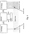
- a generic reading arrangement based on the use of a reference cell is showm in Figure 1. Its principle is that of having a generic selected cell (which may have a high or a low threshold) compared with a constantly virgin cell which, as such, will always be drawing the nominal current that characterizes it.
- the reason why reading is performed by comparing a selected cell with a reference cell is that it provides an always virgin cell capable of accommodating the process variations of the array cells throughout the integrated circuit fabrication.
- Reading by the reference cell technique actually is not effected by comparing any selected cell with one reference cell, but rather by relating the bit line that contains the cell to be read to the reference bit line.
- decoding will result in two cells being selected in the same row of the array, namely the cell to be read and the reference cell.
- the comparison is made with only one reference cell, the term reference bit line is more appropriate.
- the reference bit line does solve the problems from process variations.
- the reference bit line approach in fact, lowers the rate of variations from processing tolerances in the physical and electrical parameters between cells as brought about by the memory array being spread over a fairly large surface.
- the drains of several thousands of memory cells As mentioned above, connected to the bit lines are, especially in high storage capacity (4Mbit, 16 Mbit) devices, the drains of several thousands of memory cells. The capacitances of the junctions associated with the drains of such cells add together into an overall capacitive load of several picofarads. Again, the high bit line capacity is bound to restrict the sensing speed of any reading scheme based on the amplification of a voltage signal developed at the drain of the selected cell (voltage mode operation).
- the data discriminating circuitry should have a low input impedance and be responsive to current, rather than voltage, signals.
- the advantage of this method resides basically in its low input impedance allowing the cell current to be injected into the sense amplifier without the bit line voltage undergoing any significant change.
- the current method enables the bit line capacitance to be allocated to a node which bears little or no influence on the stored data sensing speed.
- a "pre-charging" step is also carried out in order to attain optimum voltage at the bit line node for performing the reading.
- Reading a cell which has the same threshold voltage as the reference cell includes a privileged reading and a difficult reading. Where the selected cell has a high threshold voltage (and, therefore, no current flowing therethrough), the comparison with the reference cell is easily carried out. With two cells having low thresholds, on the other hand, the comparison becomes more difficult; the current flowing through the two cells is the same, and the sensing circuitry is to detect this condition.
- the technical problem underlying the present invention is to provide a novel read circuit for semiconductor memory cells, which is based on the reference cell method and, additionally to including the best features of conventional circuits, exhibits improved accuracy in discriminating data contained in a cell, while being specifically suitable for use in multi-level cell storage devices.
- Shown in Figure 2 is a read circuit for non-volatile memory cells which is based on having capacitors charged through current mirrors, and in which the current of the reference cell(s) and the array cell is mirrored onto the capacitors.
- the principle underlying this reading technique is to arrange for capacitors to be charged, after being discharged during the step of pre-charging the bit lines which contain the reference cells and the memory cells in the array.
- the reading operation includes two distinct steps: a first step is the so-called pre-charging step whereby the reference bit line and the memory array bit line are charged to a voltage of 1 volt in order to bring the memory cell to be read to an optimum current supply condition; the second step is the reading step proper and, according to the technique being used, may be carried out in either a voltage or a current mode.
- a circuit according to the invention utilizes this technique in that the array cell and reference cell currents are mirrored onto two capacitors CR and CM which, according to the known law of capacitor charging, begin to produce increasing voltages at nodes outref and outsel (see Figure 1) depending on the current value delivered by the two cells.
- the circuit will be inhibiting the sensing structure, whose P-channel transistor M 1 and N-channel transistors M PR and M PM actually serve as switches to provide a ground connection for the nodes outref and outsel at the same time as the currents from the bit lines are being mirrored during the pre-charging step.
- the reading step begins; the sensing circuit is enabled and transistors MSR and MSM, being enabled by MI, can mirror the currents I ref and I cell from the respective reference and array branches.
- the two capacitors begin to be charged and, according to the current value being delivered from the mirrors, their voltage values will increase in different ways.
- the voltage at the node outsel will increase at a faster rate than that at the node outref.
- This evolution of the signal allows for the use of a fairly simple output structure AMP, out, such as a differential amplifier or the like, which combines enhanced circuit compactness with correspondingly high accuracy and speed of operation.
- the size of the capacitors CR and CM is highly important; in fact, too low a capacitance value would result in excessively fast, and hence inherently inaccurate, charging due to sensitivity to variations in the integration process. Conversely, high capacitance values would not only result in too slow a reading operation, but also in unacceptably high silicon area occupation. Accordingly, a compromise must be struck between speed and integration area requirements on the one side, and accuracy on the other.
- an important feature of the invention is the provision of the transistors MLR and MLM in the circuit shown in Figure 2. From the time the trailing edge of the signal ck initiates the reading step, the capacitors begin to be charged and the nodes outref and outsel to rise in voltage; of course, the rising times are different, and one of the two nodes will be first to attain a voltage (threshold voltage) driving the transistor connected to the opposite branch to discharge the slower circuit counterpart.
- the capacitor CM will be charged at a faster rate than the capacitor CR, to result in a faster increase of the voltage at the node outsel than at outref.
- the threshold voltage of the transistor MLR the latter will tend to go on and discharge the capacitor CR. Since CR already becomes charged at a slower rate because of the smaller current mirrored by the reference cell, the process will be further slowed by CR being discharged through MR.
- the two nodes in the steady-state will be at logic values of potentials Vdd and gnd, with the big advantage that the next cascaded differential stage is able to output the data in a stable manner without resorting to structures for storing the reading performed and related read or strobe signals for driving them.
- this type of sensing is based more on the capacitor charging than the operation of the cross structure of the transistors MLR and MLM.
- the sensing itself is effected during the charging.
- the transistors MLR and MLM serve to keep the data stable and prevent the capacitor that is discharging at a slower rate from attaining the charging asymptote.
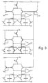
- the proposed circuit can be used with two-level cells of the standard type as well as with cells of the new multi-level type.
- the reference is represented by a memory cell whence an intermediate current is flowing between the maximum value delivered by the cell and zero; in this way, when the comparison is effected between a cell which is delivering no current and the reference cell, the latter will tend to charge the reference capacitor CR at a faster rate, whereas the steady-state capacitor CM is in a discharged state.
- the array cell is virgin, it will tend to discharge the capacitor CM at a faster rate to give rise to the opposite situation from that previously described.
- references should be programmed with suitable threshold values such that the cells led to them can deliver currents having intermediate values to the values that the generic array cell can take.
- FIG. 3 Shown in Figure 3 is the circuit structure of this invention for this example of a four-level reading.
- the present sense circuit can also be used for multi-level readings of the serial and serial dichotomic types [C. Calligaro, V. Daniele, R. Gastaldi, A. Manstretta, C. Torelli, "Serial dichotomic method for sensing multiple levels non-volatile memory cells, and sensing circuit acting such method"; C. Calligaro, V. Daniele, R. Gastaldi, N. Telecco, A. Manstretta, C. Torelli, "Sensing circuit for serial dichotomic sensing of multiple levels non-volatile memory cells", Pat. Dep. SGS-Thomson, Europe (FR DE GB IT), No. 95830110.3 (1995)], although the parallel-type technique just described is the most natural.
- the proposed circuit has the following novel features:
Landscapes
- Engineering & Computer Science (AREA)
- Computer Hardware Design (AREA)
- Read Only Memory (AREA)
- Static Random-Access Memory (AREA)
Priority Applications (5)
| Application Number | Priority Date | Filing Date | Title |
|---|---|---|---|
| EP96830494A EP0833340B1 (de) | 1996-09-30 | 1996-09-30 | Leseschaltung für Halbleiter-Speicherzellen |
| DE69627152T DE69627152T2 (de) | 1996-09-30 | 1996-09-30 | Leseschaltung für Halbleiter-Speicherzellen |
| US08/940,115 US5883837A (en) | 1996-09-30 | 1997-09-29 | Reading circuit for semiconductor memory cells |
| JP26378197A JPH10112197A (ja) | 1996-09-30 | 1997-09-29 | 半導体メモリセルの読み取り回路 |
| US09/203,798 US5973966A (en) | 1996-09-30 | 1998-12-01 | Reading circuit for semiconductor memory cells |
Applications Claiming Priority (1)
| Application Number | Priority Date | Filing Date | Title |
|---|---|---|---|
| EP96830494A EP0833340B1 (de) | 1996-09-30 | 1996-09-30 | Leseschaltung für Halbleiter-Speicherzellen |
Publications (2)
| Publication Number | Publication Date |
|---|---|
| EP0833340A1 true EP0833340A1 (de) | 1998-04-01 |
| EP0833340B1 EP0833340B1 (de) | 2003-04-02 |
Family
ID=8226017
Family Applications (1)
| Application Number | Title | Priority Date | Filing Date |
|---|---|---|---|
| EP96830494A Expired - Lifetime EP0833340B1 (de) | 1996-09-30 | 1996-09-30 | Leseschaltung für Halbleiter-Speicherzellen |
Country Status (4)
| Country | Link |
|---|---|
| US (2) | US5883837A (de) |
| EP (1) | EP0833340B1 (de) |
| JP (1) | JPH10112197A (de) |
| DE (1) | DE69627152T2 (de) |
Cited By (3)
| Publication number | Priority date | Publication date | Assignee | Title |
|---|---|---|---|---|
| EP1225595A1 (de) * | 2001-01-15 | 2002-07-24 | STMicroelectronics S.r.l. | Verfahren und Schaltung zum dynamischen Auslesen einer Speicherzelle, insbesondere einer nichtflüchtigen Multibitspeicherzelle |
| US6724658B2 (en) | 2001-01-15 | 2004-04-20 | Stmicroelectronics S.R.L. | Method and circuit for generating reference voltages for reading a multilevel memory cell |
| US6728141B2 (en) | 2001-04-19 | 2004-04-27 | Stmicroelectronics S.R.L. | Method and circuit for timing dynamic reading of a memory cell with control of the integration time |
Families Citing this family (16)
| Publication number | Priority date | Publication date | Assignee | Title |
|---|---|---|---|---|
| US5931898A (en) * | 1997-02-25 | 1999-08-03 | Lucent Technologies Inc | Finite impulse response filter |
| KR100283029B1 (ko) * | 1997-12-29 | 2001-03-02 | 윤종용 | 반도체 메모리 장치의 워드 라인 전압 발생 회로 |
| DE69827109D1 (de) * | 1998-02-13 | 2004-11-25 | St Microelectronics Srl | Abfühlverstärker für nichtflüchtigen Speicher mit niedriger Spannung |
| US6282145B1 (en) | 1999-01-14 | 2001-08-28 | Silicon Storage Technology, Inc. | Array architecture and operating methods for digital multilevel nonvolatile memory integrated circuit system |
| DE29912015U1 (de) * | 1999-07-09 | 1999-09-16 | Chang, Chien-Kuo, Taichung | Arbeitstisch |
| FR2801419B1 (fr) * | 1999-11-18 | 2003-07-25 | St Microelectronics Sa | Procede et dispositif de lecture pour memoire en circuit integre |
| US7042783B2 (en) * | 2003-06-18 | 2006-05-09 | Hewlett-Packard Development Company, L.P. | Magnetic memory |
| US7324374B2 (en) * | 2003-06-20 | 2008-01-29 | Spansion Llc | Memory with a core-based virtual ground and dynamic reference sensing scheme |
| US7345512B2 (en) | 2004-05-04 | 2008-03-18 | Silicon Storage Technology, Inc. | Sense amplifier for low voltage high speed sensing |
| US7158431B2 (en) | 2005-03-28 | 2007-01-02 | Silicon Storage Technology, Inc. | Single transistor sensing and double transistor sensing for flash memory |
| TWI402847B (zh) * | 2007-06-25 | 2013-07-21 | Higgs Opl Capital Llc | 相變化記憶體之感測電路 |
| TWI347607B (en) | 2007-11-08 | 2011-08-21 | Ind Tech Res Inst | Writing system and method for a phase change memory |
| TWI402845B (zh) | 2008-12-30 | 2013-07-21 | Higgs Opl Capital Llc | 相變化記憶體陣列之驗證電路及方法 |
| TWI412124B (zh) | 2008-12-31 | 2013-10-11 | Higgs Opl Capital Llc | 相變化記憶體 |
| US9567825B2 (en) | 2015-04-28 | 2017-02-14 | Thru Tubing Solutions, Inc. | Flow control in subterranean wells |
| CN112863584A (zh) * | 2019-11-28 | 2021-05-28 | 长鑫存储技术有限公司 | 一次可编程存储器的读写电路 |
Citations (2)
| Publication number | Priority date | Publication date | Assignee | Title |
|---|---|---|---|---|
| EP0491105A1 (de) * | 1990-12-13 | 1992-06-24 | STMicroelectronics S.r.l. | Verbesserte Abfühlschaltung für Speicheranordnungen, wie nichtflüchtige Speicher, mit verbesserter Abfühlunterscheidung |
| EP0678871A1 (de) * | 1994-03-22 | 1995-10-25 | STMicroelectronics S.r.l. | Anordnung zum Lesen einer Speicherzellenmatrix |
Family Cites Families (5)
| Publication number | Priority date | Publication date | Assignee | Title |
|---|---|---|---|---|
| IT1246241B (it) * | 1990-02-23 | 1994-11-17 | Sgs Thomson Microelectronics | Circuito per la lettura dell'informazione contenuta in celle di memoria non volatili |
| EP0700049A1 (de) * | 1994-08-31 | 1996-03-06 | STMicroelectronics S.r.l. | Leseschaltung für Speicherzellen |
| DE69526336D1 (de) * | 1995-04-28 | 2002-05-16 | St Microelectronics Srl | Leseschaltung für Speicherzellen mit niedriger Versorgungsspannung |
| US5748534A (en) * | 1996-03-26 | 1998-05-05 | Invox Technology | Feedback loop for reading threshold voltage |
| US5787042A (en) * | 1997-03-18 | 1998-07-28 | Micron Technology, Inc. | Method and apparatus for reading out a programmable resistor memory |
-
1996
- 1996-09-30 DE DE69627152T patent/DE69627152T2/de not_active Expired - Fee Related
- 1996-09-30 EP EP96830494A patent/EP0833340B1/de not_active Expired - Lifetime
-
1997
- 1997-09-29 JP JP26378197A patent/JPH10112197A/ja active Pending
- 1997-09-29 US US08/940,115 patent/US5883837A/en not_active Expired - Lifetime
-
1998
- 1998-12-01 US US09/203,798 patent/US5973966A/en not_active Expired - Lifetime
Patent Citations (2)
| Publication number | Priority date | Publication date | Assignee | Title |
|---|---|---|---|---|
| EP0491105A1 (de) * | 1990-12-13 | 1992-06-24 | STMicroelectronics S.r.l. | Verbesserte Abfühlschaltung für Speicheranordnungen, wie nichtflüchtige Speicher, mit verbesserter Abfühlunterscheidung |
| EP0678871A1 (de) * | 1994-03-22 | 1995-10-25 | STMicroelectronics S.r.l. | Anordnung zum Lesen einer Speicherzellenmatrix |
Cited By (4)
| Publication number | Priority date | Publication date | Assignee | Title |
|---|---|---|---|---|
| EP1225595A1 (de) * | 2001-01-15 | 2002-07-24 | STMicroelectronics S.r.l. | Verfahren und Schaltung zum dynamischen Auslesen einer Speicherzelle, insbesondere einer nichtflüchtigen Multibitspeicherzelle |
| US6643179B2 (en) | 2001-01-15 | 2003-11-04 | Stmicroelectronics S.R.L. | Method and circuit for dynamic reading of a memory cell, in particular a multi-level nonvolatile memory cell |
| US6724658B2 (en) | 2001-01-15 | 2004-04-20 | Stmicroelectronics S.R.L. | Method and circuit for generating reference voltages for reading a multilevel memory cell |
| US6728141B2 (en) | 2001-04-19 | 2004-04-27 | Stmicroelectronics S.R.L. | Method and circuit for timing dynamic reading of a memory cell with control of the integration time |
Also Published As
| Publication number | Publication date |
|---|---|
| DE69627152D1 (de) | 2003-05-08 |
| EP0833340B1 (de) | 2003-04-02 |
| US5883837A (en) | 1999-03-16 |
| US5973966A (en) | 1999-10-26 |
| DE69627152T2 (de) | 2004-03-04 |
| JPH10112197A (ja) | 1998-04-28 |
Similar Documents
| Publication | Publication Date | Title |
|---|---|---|
| EP0833340B1 (de) | Leseschaltung für Halbleiter-Speicherzellen | |
| USRE37072E1 (en) | Method of multi-level storage in DRAM and apparatus thereof | |
| US3967252A (en) | Sense AMP for random access memory | |
| KR920008245B1 (ko) | 불휘발성 반도체기억장치 | |
| US4070590A (en) | Sensing circuit for memory cells | |
| US4351034A (en) | Folded bit line-shared sense amplifiers | |
| US5790466A (en) | Multiple precharging semiconductor memory device | |
| US4622655A (en) | Semiconductor memory | |
| US4631707A (en) | Memory circuit with power supply voltage detection means | |
| US5592428A (en) | Dynamic memory | |
| US6137732A (en) | Semiconductor memory device having voltage boosting circuit | |
| US4338679A (en) | Row driver circuit for semiconductor memory | |
| KR19990057797A (ko) | 강유전체 메모리 장치 및 그의 읽기 방법 | |
| US5796651A (en) | Memory device using a reduced word line voltage during read operations and a method of accessing such a memory device | |
| US5917767A (en) | Semiconductor storage device | |
| US4602355A (en) | Memory circuit with noise preventing means for word lines | |
| US5745401A (en) | High-speed programmable read only memory | |
| US4255679A (en) | Depletion load dynamic sense amplifier for MOS random access memory | |
| US5402379A (en) | Precharge device for an integrated circuit internal bus | |
| EP1324344B1 (de) | Leseverstärkerstruktur für nichtflüchtige Multibitspeicheranordnungen und dazugehöriges Leseverfahren | |
| US5418748A (en) | Bit line load circuit for semiconductor static RAM | |
| EP0430455B1 (de) | Nichtflüchtige Speicheranordnung und Betriebsverfahren | |
| US4926379A (en) | Data read circuit for use in semiconductor memory device | |
| USRE32682E (en) | Folded bit line-shared sense amplifiers | |
| US6442069B1 (en) | Differential signal path for high speed data transmission in flash memory |
Legal Events
| Date | Code | Title | Description |
|---|---|---|---|
| PUAI | Public reference made under article 153(3) epc to a published international application that has entered the european phase |
Free format text: ORIGINAL CODE: 0009012 |
|
| AK | Designated contracting states |
Kind code of ref document: A1 Designated state(s): DE FR GB IT |
|
| RAP3 | Party data changed (applicant data changed or rights of an application transferred) |
Owner name: STMICROELECTRONICS S.R.L. |
|
| 17P | Request for examination filed |
Effective date: 19980922 |
|
| AKX | Designation fees paid |
Free format text: DE FR GB IT |
|
| RBV | Designated contracting states (corrected) |
Designated state(s): DE FR GB IT |
|
| GRAG | Despatch of communication of intention to grant |
Free format text: ORIGINAL CODE: EPIDOS AGRA |
|
| 17Q | First examination report despatched |
Effective date: 20020523 |
|
| GRAG | Despatch of communication of intention to grant |
Free format text: ORIGINAL CODE: EPIDOS AGRA |
|
| GRAH | Despatch of communication of intention to grant a patent |
Free format text: ORIGINAL CODE: EPIDOS IGRA |
|
| GRAH | Despatch of communication of intention to grant a patent |
Free format text: ORIGINAL CODE: EPIDOS IGRA |
|
| GRAA | (expected) grant |
Free format text: ORIGINAL CODE: 0009210 |
|
| AK | Designated contracting states |
Designated state(s): DE FR GB IT |
|
| REG | Reference to a national code |
Ref country code: GB Ref legal event code: FG4D |
|
| REF | Corresponds to: |
Ref document number: 69627152 Country of ref document: DE Date of ref document: 20030508 Kind code of ref document: P |
|
| ET | Fr: translation filed | ||
| PLBE | No opposition filed within time limit |
Free format text: ORIGINAL CODE: 0009261 |
|
| STAA | Information on the status of an ep patent application or granted ep patent |
Free format text: STATUS: NO OPPOSITION FILED WITHIN TIME LIMIT |
|
| 26N | No opposition filed |
Effective date: 20040105 |
|
| PGFP | Annual fee paid to national office [announced via postgrant information from national office to epo] |
Ref country code: DE Payment date: 20040826 Year of fee payment: 9 |
|
| PG25 | Lapsed in a contracting state [announced via postgrant information from national office to epo] |
Ref country code: IT Free format text: LAPSE BECAUSE OF NON-PAYMENT OF DUE FEES;WARNING: LAPSES OF ITALIAN PATENTS WITH EFFECTIVE DATE BEFORE 2007 MAY HAVE OCCURRED AT ANY TIME BEFORE 2007. THE CORRECT EFFECTIVE DATE MAY BE DIFFERENT FROM THE ONE RECORDED. Effective date: 20050930 |
|
| PG25 | Lapsed in a contracting state [announced via postgrant information from national office to epo] |
Ref country code: DE Free format text: LAPSE BECAUSE OF NON-PAYMENT OF DUE FEES Effective date: 20060401 |
|
| PGFP | Annual fee paid to national office [announced via postgrant information from national office to epo] |
Ref country code: GB Payment date: 20080827 Year of fee payment: 13 |
|
| PGFP | Annual fee paid to national office [announced via postgrant information from national office to epo] |
Ref country code: FR Payment date: 20080929 Year of fee payment: 13 |
|
| GBPC | Gb: european patent ceased through non-payment of renewal fee |
Effective date: 20090930 |
|
| REG | Reference to a national code |
Ref country code: FR Ref legal event code: ST Effective date: 20100531 |
|
| PG25 | Lapsed in a contracting state [announced via postgrant information from national office to epo] |
Ref country code: FR Free format text: LAPSE BECAUSE OF NON-PAYMENT OF DUE FEES Effective date: 20090930 |
|
| PG25 | Lapsed in a contracting state [announced via postgrant information from national office to epo] |
Ref country code: GB Free format text: LAPSE BECAUSE OF NON-PAYMENT OF DUE FEES Effective date: 20090930 |