EP0830666B1 - Affichage adresse par plasma - Google Patents
Affichage adresse par plasma Download PDFInfo
- Publication number
- EP0830666B1 EP0830666B1 EP97901238A EP97901238A EP0830666B1 EP 0830666 B1 EP0830666 B1 EP 0830666B1 EP 97901238 A EP97901238 A EP 97901238A EP 97901238 A EP97901238 A EP 97901238A EP 0830666 B1 EP0830666 B1 EP 0830666B1
- Authority
- EP
- European Patent Office
- Prior art keywords
- electrodes
- plasma
- data
- display device
- groups
- Prior art date
- Legal status (The legal status is an assumption and is not a legal conclusion. Google has not performed a legal analysis and makes no representation as to the accuracy of the status listed.)
- Expired - Lifetime
Links
Images


Classifications
-
- G—PHYSICS
- G09—EDUCATION; CRYPTOGRAPHY; DISPLAY; ADVERTISING; SEALS
- G09F—DISPLAYING; ADVERTISING; SIGNS; LABELS OR NAME-PLATES; SEALS
- G09F9/00—Indicating arrangements for variable information in which the information is built-up on a support by selection or combination of individual elements
- G09F9/30—Indicating arrangements for variable information in which the information is built-up on a support by selection or combination of individual elements in which the desired character or characters are formed by combining individual elements
- G09F9/35—Indicating arrangements for variable information in which the information is built-up on a support by selection or combination of individual elements in which the desired character or characters are formed by combining individual elements being liquid crystals
-
- G—PHYSICS
- G02—OPTICS
- G02F—OPTICAL DEVICES OR ARRANGEMENTS FOR THE CONTROL OF LIGHT BY MODIFICATION OF THE OPTICAL PROPERTIES OF THE MEDIA OF THE ELEMENTS INVOLVED THEREIN; NON-LINEAR OPTICS; FREQUENCY-CHANGING OF LIGHT; OPTICAL LOGIC ELEMENTS; OPTICAL ANALOGUE/DIGITAL CONVERTERS
- G02F1/00—Devices or arrangements for the control of the intensity, colour, phase, polarisation or direction of light arriving from an independent light source, e.g. switching, gating or modulating; Non-linear optics
- G02F1/01—Devices or arrangements for the control of the intensity, colour, phase, polarisation or direction of light arriving from an independent light source, e.g. switching, gating or modulating; Non-linear optics for the control of the intensity, phase, polarisation or colour
- G02F1/13—Devices or arrangements for the control of the intensity, colour, phase, polarisation or direction of light arriving from an independent light source, e.g. switching, gating or modulating; Non-linear optics for the control of the intensity, phase, polarisation or colour based on liquid crystals, e.g. single liquid crystal display cells
- G02F1/133—Constructional arrangements; Operation of liquid crystal cells; Circuit arrangements
- G02F1/1333—Constructional arrangements; Manufacturing methods
- G02F1/13334—Plasma addressed liquid crystal cells [PALC]
-
- G—PHYSICS
- G09—EDUCATION; CRYPTOGRAPHY; DISPLAY; ADVERTISING; SEALS
- G09G—ARRANGEMENTS OR CIRCUITS FOR CONTROL OF INDICATING DEVICES USING STATIC MEANS TO PRESENT VARIABLE INFORMATION
- G09G3/00—Control arrangements or circuits, of interest only in connection with visual indicators other than cathode-ray tubes
- G09G3/20—Control arrangements or circuits, of interest only in connection with visual indicators other than cathode-ray tubes for presentation of an assembly of a number of characters, e.g. a page, by composing the assembly by combination of individual elements arranged in a matrix no fixed position being assigned to or needed to be assigned to the individual characters or partial characters
- G09G3/34—Control arrangements or circuits, of interest only in connection with visual indicators other than cathode-ray tubes for presentation of an assembly of a number of characters, e.g. a page, by composing the assembly by combination of individual elements arranged in a matrix no fixed position being assigned to or needed to be assigned to the individual characters or partial characters by control of light from an independent source
- G09G3/36—Control arrangements or circuits, of interest only in connection with visual indicators other than cathode-ray tubes for presentation of an assembly of a number of characters, e.g. a page, by composing the assembly by combination of individual elements arranged in a matrix no fixed position being assigned to or needed to be assigned to the individual characters or partial characters by control of light from an independent source using liquid crystals
- G09G3/3611—Control of matrices with row and column drivers
- G09G3/3648—Control of matrices with row and column drivers using an active matrix
- G09G3/3662—Control of matrices with row and column drivers using an active matrix using plasma-addressed liquid crystal displays
Definitions
- This invention relates to a plasma-addressed display device for displaying a matrix of M rows of N pixels wherein N is larger than M, the display device comprising: a layer of electro-optical material sandwiched between elongated data electrodes and plasma channels, the data electrodes and the plasma channels crossing each other for obtaining overlapping areas constituting pixelelements corresponding to the pixels, each plasma channel comprising spaced first and second electrodes, a plasma driver circuit coupled to the first and the second electrodes for selectively activating the plasma channels for selecting pixelelements associated with the activated plasma channel, the first electrodes being interconnected in a number of first groups and the second electrodes being interconnected in a number of second groups such that each of the first groups includes no more than one electrode of each of the second groups, and a data driver circuit coupled to the data electrodes for supplying data signals to the pixelelements in response to a video information.
- EP-B-0,325,387 discloses a plasma-addressed liquid crystal display, commonly referred to as a "PALC" display device.
- the known PALC display device comprises: a first substrate on which parallel transparent column electrodes are deposited, a second substrate which has parallel sealed plasma channels corresponding to rows of the display, and an electro-optical material such as a liquid crystal material sandwiched between the substrates.
- Each of the plasma channels of the second substrate is filled with a low pressure ionizable gas, such as helium, and contains spaced cathode and anode electrodes along the channel for ionizing the gas to create a conductive plasma.
- the channels are closed off by a thin transparent dielectric sheet.
- Each of the plasma channels crosses all of the column electrodes to form a matrix of overlapping regions. The overlapping regions correspond to pixels of the electro-optical material.
- the operation of the PALC display device is, by way of example, further elucidated in case the electro-optical material is liquid crystal material (LC-material).
- the plasma channel acts as a row switch capable of selectively addressing a row of liquid crystal pixel elements (LC-pixels). Successive lines of data signals representing an image to be displayed are sampled at column positions and the sampled data voltages are respectively applied to the column electrodes. All but one of the row plasma channels are in the deionized or non-conducting state.
- the plasma of the one ionized selected plasma channel is conducting and, in effect, establishes a reference potential on the adjacent side of a row of LC-pixels, causing each LC-pixel to charge to the difference of the reference potential and the column potential.
- the ionized channel is turned off for isolating the LC-pixel charge and storing the data voltage for a frame period.
- the next row of data appears on the column electrodes, only the succeeding plasma channel row is ionized to store the data voltages in the succeeding row of LC-pixels, and so on.
- the attenuation of each LC-pixel to backlight or incident light is a function of the stored voltage across the pixel.
- the first possibility shows that one electrode of each plasma channel is connected to a reference potential. So, all these electrodes can be interconnected to receive the reference potential. The remaining electrode of each plasma channel is connected to receive a pulse signal.
- the plasma channels are selected one by one by supplying one pulse signal with a voltage pulse which has a value with respect to the reference voltage that is large enough to ionize the plasma, while all other pulse signals supply a voltage which has a value with respect to the reference voltage that is too low to ionize the plasma. Assuming a PALC display device with N rows of pixels, N pulse drivers are needed to supply the N pulse signals to the panel.
- Such a panel has 2N connections for supplying the pulse signals and the reference voltage to the electrodes of the plasma channels.
- the second possibility shows that the number of pulse drivers decreases by taking together in groups both the anode and the cathode electrodes.
- the groups are chosen such that each of the anode groups includes no more than one electrode of each of the cathode groups, and in the same way, each of the cathode groups includes no more than one electrode of each of the anode groups.
- the adjacent cathode-anode electrode pairs are each located in one channel, and the channels whose electrodes form any one of a first group thus include no more than one electrode of any one of the second group.
- both the cathode and anode electrodes are taken together in groups of N 1 ⁇ 2 lines, with one pulse driver per group. This leads to 2N 1 ⁇ 2 instead of N pulse drivers, and if the connections in each of the groups is made on the PALC display panel to 2N 1 ⁇ 2 instead of 2N connections.
- the known display device has as a drawback that still a lot of data drivers are needed to supply the data signals to the column electrodes.
- An aspect of the invention is characterized in that the data electrodes are arranged to constitute the M rows, the plasma channels are arranged to constitute N columns, and the data driver circuit is adapted to supply data signals to a column of selected pixelelements.
- the invention is based on the insight that, in practise, PALC displays contain more pixels per row than rows. The total number of connections can be lowered by transposing the display such that the plasma channels constitute the columns, and the former column electrodes now constitute the rows. The former column electrodes further will be referred to as data electrodes to avoid confusion about "column" electrodes extending in the row direction. Now a conductive plasma channel selects a column instead of a row of pixel elements.
- the video signal is supplied to a column of selected pixels instead to a row of selected pixels. If the video signal comprises frames of lines, as is usually the case, a video transposing circuit is needed to transpose the video information. If the video signal is generated by a computer video card which uses memory to store the video information, the circuitry controlling the memory has to be adapted to transpose the video information.
- the following example elucidates that the measure of the invention decreases the total number of drivers needed to supply drive signals to the PALC display panel.
- a known PALC display with an aspect ratio of 3:4 would have 1200 rows (plasma channels) and 1600 columns (data electrodes).
- the total number of drivers is not less than about 1670, viz. 2*1200 1 ⁇ 2 for driving the anode and cathode groups and 1600 for driving the data electrodes.
- a corresponding PALC display according to the invention has 1200 data rows and 1600 plasma channels.
- the total number of drivers is only 1280, viz. 2*1600 1 ⁇ 2 for driving the anode and cathode groups and 1200 for driving the data electrodes.
- the invention may offer even a more substantial decrease in the total number of drivers for the new displays with an aspect ratio of 16:9 in which the number of pixels in a row is likely to be even much more larger than the number of rows.
- the decreased number of data electrodes has the further advantage that the spacing between the connections to the data electrodes becomes larger.
- first and second electrodes As for the ignition of the plasma it is only important to supply a large enough voltage difference between the anode and cathode electrodes it is possible to interchange the position of the anode and cathode electrodes. Therefor these electrodes are also referred to as first and second electrodes.
- a video transposing circuit and a transposed liquid crystal display are known from US-A-5,267,045.
- This known art discloses a video circuit adapted to enable the display of video information of various television standards which have a different number of lines per frame on a liquid crystal display, further referred to as LCD, which has a fixed number of rows.
- the video circuit comprises a memory, and reads in the video information in the row direction, and subsequently reads out the video information in the column direction with an adaptable clock rate.
- the readout video information is presented to the rows of a transposed LCD.
- the embodiment according to claim 3 constitutes a group of pixels by using three plasma channels in column direction crossed by one data electrode in row direction. Now, the colour filters are aligned with the plasma channels.
- a plasma driver circuit connected to the groups of anode and cathode electrodes has to be adapted to sequentially scan the three plasma channels in a group.
- a data driver circuit connected to the data electrodes has to be adapted to supply the data signals belonging to the three colours sequentially to the common data electrode such that the data of a specific colour is presented to the activated plasma channel associated to a colour filter corresponding to that colour. In this way the number of data electrodes and thus the number of connections thereto reduces by a factor three.
- the PALC display according to the invention comprises 1200 data electrodes extending in the row direction and 3*1600 plasma channels extending in the column direction.
- the total number of drivers is only about 1339, viz. 2*(3*1600) 1 ⁇ 2 for the anode and cathode groups and 1200 for the data electrodes, which is significantly lower than the 4870 drivers needed in the known PALC display. If the interconnections between cathode and anode electrodes, respectively are made on the PALC panel, also the number of connections decreases with the same amount.
- Fig. 1 and Fig. 2 are used in combination to explain the construction and the electronic circuitry to drive a conventional PALC display.
- Fig. 1 shows a flat panel display system 10, which represents a typical PALC display device.
- the flat panel display system comprises a display panel 12 having a display surface 14 which contains a pattern formed by a rectangular planar array of nominally identical data storage or display elements 16 (also referred to as pixels) mutually spaced apart by predetermined distances in the vertical and horizontal directions.
- Each display element 16 in the array represents the overlapping portions of thin, narrow electrodes 18 arranged in vertical columns and elongate, narrow plasma channels 20 arranged in horizontal rows.
- the electrodes 18 are hereinafter also referred to as "column electrodes").
- the display elements 16 associated with one of the channels 20 represent one line of data of a video information V.
- the widths of column electrodes 18 and channels 20 determine the dimensions of display elements 16, which are typically of rectangular shape.
- Column electrodes 18 are deposited on a major surface of a first electrically nonconductive, optically transparent substrate 34 (see Figure 2), and the plasma channel rows are usually built into a second transparent substrate 36.
- An electro-optical material 42 such as a liquid crystal (LC) material is located between the substrates 34 and 36.
- LC liquid crystal
- the column electrodes 18 receive data drive signals developed on parallel output conductors 22' by output amplifiers 23 (Fig. 2) of a data driver circuit 24 which receives the video information V.
- the channels 20 receive data strobe signals of the voltage pulse type developed on parallel output conductors 26' by output amplifiers 21 (Fig. 2) of a plasma driver circuit 28.
- a cathode electrode 30 (Fig. 2) and an anode electrode 31 are provided in each of the channels 20.
- display system 10 employs a scan control circuit 32 that coordinates the functions of the data driver circuit 24 and the plasma driver circuit 28 so that all columns of display elements 16 of display panel 12 are addressed row by row.
- Display panel 12 may employ electro-optical materials 42 of different types. For example, if it uses such material that changes the polarization state of incident light rays, display panel 12 is positioned between a pair of light polarizing filters, which cooperate with display panel 12 to change the luminance of light propagating through them. The use of a scattering liquid crystal cell as the electro-optical material would not require the use of polarizing filters, however.
- LC materials are presently the most common example, the detailed description will refer to LC materials but it will be understood that the invention is not limited to display panels with liquid crystal materials.
- Fig. 2 illustrates a PALC display panel using LC material. Only a few column electrodes 18 and plasma channels 20 are shown.
- the rows of the PALC display panel are constituted by a plurality of parallel elongated sealed plasma channels 20 underlying a layer 42 of the LC material.
- Each of the plasma channels 20 is filled with an ionizable gas 44, is closed off with a thin dielectric sheet 45 typically of glass, and contains on an interior channel surface first and second spaced elongated electrodes 30, 31 which extend the full length of the plasma channel 20.
- the first electrode 30 in the prior art arrangement is typically grounded and is commonly called the cathode.
- the second electrode 31 is called the anode, because a positive strobe pulse sufficient to cause electrons to be emitted from the cathode electrode 30 to ionize the gas will typically be supplied to the anode 31 relative to the cathode electrode 30.
- each plasma channel 20 in turn, has its gas ionized with a strobe pulse to create a plasma.
- the ionized plasma has a low conductivity and connects a reference potential to a row of pixels in the LC layer 42 above.
- the strobe pulse terminates, and after deionization has occurred, the next channel is strobed and turned on. Since the column electrodes 18 each cross a whole column of pixels, only one plasma channel 20 at a time is allowed to be active (in the conductive state) to avoid crosstalk.
- Fig. 3 is a circuit schematic of a known arrangement of channel cathode 30-1,...,30- ⁇ N and anode 31-1,...,31- ⁇ N electrode connections into plural groups.
- the number of pulse drivers coupled to the connections 8,9 to a PALC display panel 12 decreases by taking together in groups both the cathode electrodes 30-1,...,30- ⁇ N and the anode electrodes 31-1,...,31- ⁇ N, such that each of the cathode groups 30-1,...,30- ⁇ N includes no more than one electrode of each of the anode 31-1,...,31- ⁇ N groups, and in the same way, each of the anode groups 31-1,...,31- ⁇ N includes no more than one electrode of each of the cathode groups 30-1,...,30- ⁇ N.
- Adjacent cathode-anode electrode pairs are located in one plasma channel 20, and the plasma channels 20 whose electrodes form any one of a first group thus include no more than one electrode of any one of the second group.
- the anode and cathode electrodes may be interconnected on the PALC display panel (as shown) to also reduce the number of connections of the PALC display panel. Assuming such a PALC display device with N rows of pixels, both the cathode electrodes 30-1,...,30- ⁇ N and anode electrodes 31-1,...,31- ⁇ N are taken together in groups of N 1 ⁇ 2 lines, with one connection 8,9 per group.
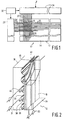
- Fig. 4 is a perspective view of part of a PALC display device according to the invention.
- the same reference numerals are referring to the same elements as in Fig. 2.
- the PALC display panel 12 is transposed such that the plasma channels 20 constitute the columns, and the former column electrodes 18 now constitute the rows.
- the electrodes 18 further will be referred to as data electrodes 18 to avoid confusion that "column" electrodes extend in the row direction.
- the cathode electrodes 30 and anode electrodes 31 are grouped together to minimize the number of pulse drivers 28 needed to activate the plasma channels 20.
- Fig. 5 is a schematic block diagram of a flat panel display system according to the invention.
- the same reference numerals are referring to the same elements as in Fig. 1.
- the plasma drive circuit 28 supplies the data strobe signals via the connections 8,9 to the grouped output conductors 26' which are connected to the cathode and anode electrodes 30,31 of each plasma channel 20.
- the grouping of the cathode and anode electrodes 30,31 is depicted by a block with reference Gc.
- the data driver circuit 24 receives the video information V and supplies the data drive signals via the parallel output conductors 22' and the output amplifiers 23 to the data electrodes 18.
- the plasma channels 20 select columns instead of rows of pixel elements 16, the video information V has to be converted to data signals which are supplied to the data electrodes 18 column-wise instead of row-wise. This necessitates a video transposing circuit 240.
- Fig. 6 is a perspective view of part of a conventional colour PALC display device as shown in the cited publication of Buzak et al..
- Three colour filters which transmit each a different primary colour are associated with three adjacent column electrodes 18 to obtain groups G of three display elements or pixels 16.
- each group of pixels is constituted by three column electrodes 18 extending in the column direction and one plasma channel 20 extending in the row direction.
- colour can also be achieved by using three separate monochrome panels 12, each of which controls one primary colour.
- the width of the column electrodes 18 could be larger than shown in Fig. 6 to obtain predominantly square pixels 16, as shown in Fig. 4.
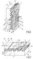
- Fig. 7 is a perspective view of part of another PALC display device according to the invention.
- the same reference numerals are referring to the same elements as in Fig. 4.
- the transposed PALC colour display device of Fig. 4 is adapted such that a group G of pixels 16 is constituted by three adjacent plasma channels 20 extending in the column direction and one associated data electrode 18 extending in the row direction.
- the number of data electrodes 18 and thus the number of connections thereto decreases with a factor three.
- the number of plasma channels 20 increases by a factor three, but the number of connections 8,9 to the plasma channels only increases with the square root. So, the total number of connections to the PALC display device further decreases.
- the invention can be used in all kinds of PALC displays, such displays typically have a small channel pitch for use in computer monitors, workstations or TV applications.
- a primary aspect of the invention relates to a plasma-addressed electro-optical display device comprising a layer of electro-optical material 42, data electrodes 18 coupled to the electro-optical layer 42 and adapted to receive data voltages for activating portions of the electro-optical layer 42, and a plurality of plasma channels 20 extending generally transverse to the data electrodes 18 for selectively switching on said electro-optical portions.
- the plasma channels 20 each comprise spaced elongated cathode and anode electrodes 30,31 and an ionizable gas filling 44.
- the cathode and anode electrodes 30,31 are arranged in groups to reduce the number of drivers 28 required to drive the cathode and anode electrodes 30,31.
- plasma channels 20 are interchanged with the data electrodes 18.
- the plasma channels 20 now extending in the column direction and the data electrodes 18 extending in the row direction.
- the video signal V to be displayed has to be converted into data signals supplied to the date electrodes 18 in a column-wise way instead of in a row-wise way.
Abstract
Claims (3)
- Dispositif d'affichage adressé par plasma pour afficher une matrice de M rangées de N pixels (16), où N est plus grand que M, le dispositif d'affichage comprenant :une couche d'un matériau électro-optique (42) prise en sandwich entre de longues électrodes de données (18) et des canaux à plasma (20), les électrodes de données (18) et les canaux à plasma (20) se coupant les uns les autres pour former des zones chevauchantes constituant des éléments de pixels correspondant aux pixels (16), chaque canal à plasma (20) comprenant une première (31) et une seconde (30) électrode espacées,un circuit de pilotage de plasma (28) couplé aux premières (31) et secondes (30) électrodes pour exciter sélectivement les canaux à plasma (20) afin de sélectionner des éléments de pixels (16) associés au canal à plasma excité (20), les premières électrodes (30) étant interconnectées en un certain nombre de premiers groupes et les secondes électrodes (31) étant interconnectées en un certain nombre de seconds groupes de telle sorte que chacun des premiers groupes ne comprenne pas plus d'une électrode de chacun des seconds groupes, etun circuit de pilotage de données (24) couplé aux électrodes de données (18) pour délivrer des signaux de données aux éléments de pixels (16) en réponse à des informations vidéo (V), caractérisé en ce que les électrodes de données (18) sont agencées pour constituer les M rangées, les canaux à plasma (20) sont agencés pour constituer N colonnes et le circuit d'excitation de données (24) est à même de délivrer des signaux de données à une colonne d'éléments de pixels choisis (16).
- Dispositif d'affichage adressé par plasma selon la revendication 1, caractérisé en ce que les informations vidéo (V) comprennent un nombre constant de lignes vidéo.
- Dispositif d'affichage adressé par plasma selon la revendication 1 ou 2, caractérisé en ce que le dispositif d'affichage comprend par ailleurs des filtres colorés, chaque filtre coloré étant aligné avec un canal à plasma (20) pour obtenir des groupes (G) d'un certain nombre d'éléments de pixels adjacents (16) représentant différentes couleurs afin de permettre l'affichage d'une image en couleurs, les groupes d'éléments de pixels (G) étant chacun constitués d'une électrode de données commune (18) coopérant avec un nombre de canaux à plasma (20) égal au nombre d'éléments de pixels (16) dans le groupe (G), le circuit de pilotage de plasma (28) étant à même d'exciter sélectivement les canaux à plasma (20) du groupe, et le circuit de pilotage de données (24) étant à même de délivrer les signaux de données en séquence à l'électrode de données commune (18).
Priority Applications (1)
| Application Number | Priority Date | Filing Date | Title |
|---|---|---|---|
| EP97901238A EP0830666B1 (fr) | 1996-03-18 | 1997-02-13 | Affichage adresse par plasma |
Applications Claiming Priority (4)
| Application Number | Priority Date | Filing Date | Title |
|---|---|---|---|
| EP96200749 | 1996-03-18 | ||
| EP96200749 | 1996-03-18 | ||
| EP97901238A EP0830666B1 (fr) | 1996-03-18 | 1997-02-13 | Affichage adresse par plasma |
| PCT/IB1997/000117 WO1997035294A1 (fr) | 1996-03-18 | 1997-02-13 | Affichage adresse par plasma |
Publications (2)
| Publication Number | Publication Date |
|---|---|
| EP0830666A1 EP0830666A1 (fr) | 1998-03-25 |
| EP0830666B1 true EP0830666B1 (fr) | 2000-05-10 |
Family
ID=8223796
Family Applications (1)
| Application Number | Title | Priority Date | Filing Date |
|---|---|---|---|
| EP97901238A Expired - Lifetime EP0830666B1 (fr) | 1996-03-18 | 1997-02-13 | Affichage adresse par plasma |
Country Status (7)
| Country | Link |
|---|---|
| US (1) | US6130655A (fr) |
| EP (1) | EP0830666B1 (fr) |
| JP (1) | JPH11506229A (fr) |
| KR (1) | KR19990014878A (fr) |
| DE (1) | DE69701941T2 (fr) |
| MY (1) | MY132453A (fr) |
| WO (1) | WO1997035294A1 (fr) |
Families Citing this family (13)
| Publication number | Priority date | Publication date | Assignee | Title |
|---|---|---|---|---|
| JP3559719B2 (ja) | 1998-01-13 | 2004-09-02 | キヤノン株式会社 | プラズマアドレス型の液晶表示装置 |
| JP4801247B2 (ja) * | 1999-10-08 | 2011-10-26 | 株式会社半導体エネルギー研究所 | 表示装置 |
| US6796867B2 (en) | 2000-10-27 | 2004-09-28 | Science Applications International Corporation | Use of printing and other technology for micro-component placement |
| US6570335B1 (en) * | 2000-10-27 | 2003-05-27 | Science Applications International Corporation | Method and system for energizing a micro-component in a light-emitting panel |
| US6545422B1 (en) * | 2000-10-27 | 2003-04-08 | Science Applications International Corporation | Socket for use with a micro-component in a light-emitting panel |
| US6620012B1 (en) | 2000-10-27 | 2003-09-16 | Science Applications International Corporation | Method for testing a light-emitting panel and the components therein |
| US6764367B2 (en) | 2000-10-27 | 2004-07-20 | Science Applications International Corporation | Liquid manufacturing processes for panel layer fabrication |
| US6822626B2 (en) | 2000-10-27 | 2004-11-23 | Science Applications International Corporation | Design, fabrication, testing, and conditioning of micro-components for use in a light-emitting panel |
| US6762566B1 (en) | 2000-10-27 | 2004-07-13 | Science Applications International Corporation | Micro-component for use in a light-emitting panel |
| US6612889B1 (en) | 2000-10-27 | 2003-09-02 | Science Applications International Corporation | Method for making a light-emitting panel |
| US6801001B2 (en) | 2000-10-27 | 2004-10-05 | Science Applications International Corporation | Method and apparatus for addressing micro-components in a plasma display panel |
| US7288014B1 (en) | 2000-10-27 | 2007-10-30 | Science Applications International Corporation | Design, fabrication, testing, and conditioning of micro-components for use in a light-emitting panel |
| US6674419B2 (en) * | 2000-11-02 | 2004-01-06 | Tektronix, Inc. | AC palc display device with floating electrode |
Family Cites Families (9)
| Publication number | Priority date | Publication date | Assignee | Title |
|---|---|---|---|---|
| US4896149A (en) * | 1988-01-19 | 1990-01-23 | Tektronix, Inc. | Addressing structure using ionizable gaseous medium |
| US5272472A (en) * | 1988-01-19 | 1993-12-21 | Tektronix, Inc. | Apparatus for addressing data storage elements with an ionizable gas excited by an AC energy source |
| DE69214206T2 (de) * | 1991-07-08 | 1997-03-13 | Asahi Glass Co Ltd | Steuerverfahren für ein Flüssigkristallanzeigeelement |
| DE69212076T2 (de) * | 1991-07-19 | 1997-01-30 | Philips Electronics Nv | Mehrnormwiedergabeanordnung |
| KR940005881B1 (ko) * | 1991-09-28 | 1994-06-24 | 삼성전관 주식회사 | 칼라 플라즈마 표시장치 |
| JP3107260B2 (ja) * | 1993-03-02 | 2000-11-06 | 株式会社富士通ゼネラル | カラー表示装置 |
| KR0160321B1 (ko) * | 1994-04-28 | 1998-12-01 | 박현승 | 평면가스표시관 |
| JPH08106080A (ja) * | 1994-10-05 | 1996-04-23 | Sony Corp | 画像表示装置 |
| US5835167A (en) * | 1994-12-21 | 1998-11-10 | Philips Electronics North America | Plasma addressed liquid crystal display with reduced column voltages |
-
1997
- 1997-02-13 WO PCT/IB1997/000117 patent/WO1997035294A1/fr active IP Right Grant
- 1997-02-13 EP EP97901238A patent/EP0830666B1/fr not_active Expired - Lifetime
- 1997-02-13 JP JP9533285A patent/JPH11506229A/ja active Pending
- 1997-02-13 KR KR1019970708223A patent/KR19990014878A/ko active IP Right Grant
- 1997-02-13 DE DE69701941T patent/DE69701941T2/de not_active Expired - Fee Related
- 1997-03-06 US US08/812,223 patent/US6130655A/en not_active Expired - Fee Related
- 1997-03-17 MY MYPI97001127A patent/MY132453A/en unknown
Also Published As
| Publication number | Publication date |
|---|---|
| DE69701941T2 (de) | 2000-12-07 |
| US6130655A (en) | 2000-10-10 |
| KR19990014878A (ko) | 1999-02-25 |
| EP0830666A1 (fr) | 1998-03-25 |
| JPH11506229A (ja) | 1999-06-02 |
| WO1997035294A1 (fr) | 1997-09-25 |
| MY132453A (en) | 2007-10-31 |
| DE69701941D1 (de) | 2000-06-15 |
Similar Documents
| Publication | Publication Date | Title |
|---|---|---|
| US5519520A (en) | AC plasma address liquid crystal display | |
| EP0830666B1 (fr) | Affichage adresse par plasma | |
| US5898416A (en) | Display device | |
| US7038668B2 (en) | Picture displaying apparatus, which does not require a calculating circuit, when the screen saver function is attained, and a method of driving the same | |
| EP0745251B1 (fr) | Formes d'ondes de tension de commande pour des affichages a cristaux liquides adresses par plasma | |
| EP0827617B1 (fr) | Afficheur couleur adresse par plasma | |
| US5627431A (en) | Electro-optical device | |
| US5835167A (en) | Plasma addressed liquid crystal display with reduced column voltages | |
| EP0746836B1 (fr) | Configuration des canaux pour un afficheur a cristaux liquides au plasma | |
| JP3013471B2 (ja) | 画像表示装置 | |
| KR19990028821A (ko) | 자동 입체 디스플레이 장치 | |
| US6233028B1 (en) | Plasma-addressed liquid crystal display with reduced column voltages | |
| JPH10148820A (ja) | プラズマ・アドレス液晶表示パネル及びそのチャンネル・サブアッセンブリ | |
| US5982096A (en) | Device having a plurality of ionizable gas filled channel in a gas-tight envelope, each channel provided with a pair of electrodes | |
| JP2794151B2 (ja) | プラズマ・アドレス指定構体 | |
| JP2000181413A (ja) | 表示装置及び表示装置の駆動方法 | |
| US5896008A (en) | Electro-optical device | |
| JP2998242B2 (ja) | 画像表示装置 | |
| JP3019042B2 (ja) | 画像表示装置 | |
| JP3013472B2 (ja) | 画像表示装置 | |
| JP3013469B2 (ja) | 画像表示装置 | |
| KR940009147B1 (ko) | 플라즈마 어드레스 방식의 액정표시소자 | |
| JPH05142523A (ja) | 画像表示装置 |
Legal Events
| Date | Code | Title | Description |
|---|---|---|---|
| PUAI | Public reference made under article 153(3) epc to a published international application that has entered the european phase |
Free format text: ORIGINAL CODE: 0009012 |
|
| AK | Designated contracting states |
Kind code of ref document: A1 Designated state(s): DE FR GB IT |
|
| 17P | Request for examination filed |
Effective date: 19980325 |
|
| GRAG | Despatch of communication of intention to grant |
Free format text: ORIGINAL CODE: EPIDOS AGRA |
|
| GRAG | Despatch of communication of intention to grant |
Free format text: ORIGINAL CODE: EPIDOS AGRA |
|
| 17Q | First examination report despatched |
Effective date: 19990407 |
|
| GRAG | Despatch of communication of intention to grant |
Free format text: ORIGINAL CODE: EPIDOS AGRA |
|
| GRAH | Despatch of communication of intention to grant a patent |
Free format text: ORIGINAL CODE: EPIDOS IGRA |
|
| GRAH | Despatch of communication of intention to grant a patent |
Free format text: ORIGINAL CODE: EPIDOS IGRA |
|
| GRAA | (expected) grant |
Free format text: ORIGINAL CODE: 0009210 |
|
| AK | Designated contracting states |
Kind code of ref document: B1 Designated state(s): DE FR GB IT |
|
| REF | Corresponds to: |
Ref document number: 69701941 Country of ref document: DE Date of ref document: 20000615 |
|
| ITF | It: translation for a ep patent filed |
Owner name: ING. C. GREGORJ S.P.A. |
|
| ET | Fr: translation filed | ||
| PLBE | No opposition filed within time limit |
Free format text: ORIGINAL CODE: 0009261 |
|
| STAA | Information on the status of an ep patent application or granted ep patent |
Free format text: STATUS: NO OPPOSITION FILED WITHIN TIME LIMIT |
|
| 26N | No opposition filed | ||
| REG | Reference to a national code |
Ref country code: GB Ref legal event code: IF02 |
|
| PGFP | Annual fee paid to national office [announced via postgrant information from national office to epo] |
Ref country code: FR Payment date: 20020222 Year of fee payment: 6 |
|
| PGFP | Annual fee paid to national office [announced via postgrant information from national office to epo] |
Ref country code: GB Payment date: 20020228 Year of fee payment: 6 |
|
| PGFP | Annual fee paid to national office [announced via postgrant information from national office to epo] |
Ref country code: DE Payment date: 20020417 Year of fee payment: 6 |
|
| PG25 | Lapsed in a contracting state [announced via postgrant information from national office to epo] |
Ref country code: GB Free format text: LAPSE BECAUSE OF NON-PAYMENT OF DUE FEES Effective date: 20030213 |
|
| PG25 | Lapsed in a contracting state [announced via postgrant information from national office to epo] |
Ref country code: DE Free format text: LAPSE BECAUSE OF NON-PAYMENT OF DUE FEES Effective date: 20030902 |
|
| GBPC | Gb: european patent ceased through non-payment of renewal fee | ||
| PG25 | Lapsed in a contracting state [announced via postgrant information from national office to epo] |
Ref country code: FR Free format text: LAPSE BECAUSE OF NON-PAYMENT OF DUE FEES Effective date: 20031031 |
|
| REG | Reference to a national code |
Ref country code: FR Ref legal event code: ST |
|
| PG25 | Lapsed in a contracting state [announced via postgrant information from national office to epo] |
Ref country code: IT Free format text: LAPSE BECAUSE OF NON-PAYMENT OF DUE FEES;WARNING: LAPSES OF ITALIAN PATENTS WITH EFFECTIVE DATE BEFORE 2007 MAY HAVE OCCURRED AT ANY TIME BEFORE 2007. THE CORRECT EFFECTIVE DATE MAY BE DIFFERENT FROM THE ONE RECORDED. Effective date: 20050213 |