EP0829767A1 - Verfahren und Vorrichtung zur Behandlung eines Photoresists - Google Patents
Verfahren und Vorrichtung zur Behandlung eines Photoresists Download PDFInfo
- Publication number
- EP0829767A1 EP0829767A1 EP97115936A EP97115936A EP0829767A1 EP 0829767 A1 EP0829767 A1 EP 0829767A1 EP 97115936 A EP97115936 A EP 97115936A EP 97115936 A EP97115936 A EP 97115936A EP 0829767 A1 EP0829767 A1 EP 0829767A1
- Authority
- EP
- European Patent Office
- Prior art keywords
- processing solution
- gas
- nozzle
- side portion
- liquid separation
- Prior art date
- Legal status (The legal status is an assumption and is not a legal conclusion. Google has not performed a legal analysis and makes no representation as to the accuracy of the status listed.)
- Granted
Links
Images


Classifications
-
- H—ELECTRICITY
- H01—ELECTRIC ELEMENTS
- H01L—SEMICONDUCTOR DEVICES NOT COVERED BY CLASS H10
- H01L21/00—Processes or apparatus adapted for the manufacture or treatment of semiconductor or solid state devices or of parts thereof
- H01L21/02—Manufacture or treatment of semiconductor devices or of parts thereof
- H01L21/027—Making masks on semiconductor bodies for further photolithographic processing not provided for in group H01L21/18 or H01L21/34
-
- G—PHYSICS
- G03—PHOTOGRAPHY; CINEMATOGRAPHY; ANALOGOUS TECHNIQUES USING WAVES OTHER THAN OPTICAL WAVES; ELECTROGRAPHY; HOLOGRAPHY
- G03F—PHOTOMECHANICAL PRODUCTION OF TEXTURED OR PATTERNED SURFACES, e.g. FOR PRINTING, FOR PROCESSING OF SEMICONDUCTOR DEVICES; MATERIALS THEREFOR; ORIGINALS THEREFOR; APPARATUS SPECIALLY ADAPTED THEREFOR
- G03F7/00—Photomechanical, e.g. photolithographic, production of textured or patterned surfaces, e.g. printing surfaces; Materials therefor, e.g. comprising photoresists; Apparatus specially adapted therefor
- G03F7/26—Processing photosensitive materials; Apparatus therefor
- G03F7/30—Imagewise removal using liquid means
- G03F7/3021—Imagewise removal using liquid means from a wafer supported on a rotating chuck
-
- B—PERFORMING OPERATIONS; TRANSPORTING
- B05—SPRAYING OR ATOMISING IN GENERAL; APPLYING FLUENT MATERIALS TO SURFACES, IN GENERAL
- B05D—PROCESSES FOR APPLYING FLUENT MATERIALS TO SURFACES, IN GENERAL
- B05D1/00—Processes for applying liquids or other fluent materials
- B05D1/002—Processes for applying liquids or other fluent materials the substrate being rotated
- B05D1/005—Spin coating
-
- B—PERFORMING OPERATIONS; TRANSPORTING
- B05—SPRAYING OR ATOMISING IN GENERAL; APPLYING FLUENT MATERIALS TO SURFACES, IN GENERAL
- B05D—PROCESSES FOR APPLYING FLUENT MATERIALS TO SURFACES, IN GENERAL
- B05D3/00—Pretreatment of surfaces to which liquids or other fluent materials are to be applied; After-treatment of applied coatings, e.g. intermediate treating of an applied coating preparatory to subsequent applications of liquids or other fluent materials
- B05D3/002—Pretreatement
-
- G—PHYSICS
- G03—PHOTOGRAPHY; CINEMATOGRAPHY; ANALOGOUS TECHNIQUES USING WAVES OTHER THAN OPTICAL WAVES; ELECTROGRAPHY; HOLOGRAPHY
- G03F—PHOTOMECHANICAL PRODUCTION OF TEXTURED OR PATTERNED SURFACES, e.g. FOR PRINTING, FOR PROCESSING OF SEMICONDUCTOR DEVICES; MATERIALS THEREFOR; ORIGINALS THEREFOR; APPARATUS SPECIALLY ADAPTED THEREFOR
- G03F7/00—Photomechanical, e.g. photolithographic, production of textured or patterned surfaces, e.g. printing surfaces; Materials therefor, e.g. comprising photoresists; Apparatus specially adapted therefor
- G03F7/16—Coating processes; Apparatus therefor
Definitions
- the present invention relates to a resist processing method for coating a resist on a substrate such as a semiconductor wafer and an LCD substrate, and developing the coated resist, and also relates to a resist processing system.
- a desired circuit pattern is formed by coating a resist on a semiconductor wafer and a substrate for a liquid crystal display (LCD), exposing the coated resist to light, and developing the exposed resist with a developing solution.
- a carrier gas pressurized N 2 gas
- the developing solution is sent out from the tank by the gas pressure by way of a supply line to a nozzle. Finally, the developing solution is expelled from the nozzle onto the substrate.
- the developing solution In such a developing process, the developing solution must be uniformly supplied over the entire substrate surface in a short time to prevent non-uniform development. If the developing solution is supplied quickly from the tank to the nozzle by increasing the pressure of the carrier gas, a large quantity of the carrier gas dissolves in the developing solution, or ambient air gets involved into the developing solution which is supplied from the nozzle. As a result, air bubbles are readily formed in the developing solution supplied to the substrate. The air bubbles attach to a substrate surface, preventing the exposure of the coated resist to the developing solution. This is a cause of the defect, "undeveloped portion of a resist". To avoid this, a deaeration apparatus has been used to separate and remove a gaseous component from the developing solution before the solution is supplied to the substrate.
- the resist processing method according to the present invention is a method for introducing a pressurized gas into a vessel storing a processing solution, sending the processing solution from the vessel to a nozzle by way of a supply line by means of the pressurized gas, and supplying the processing solution from the nozzle to a substrate, the method comprising the steps of:
- the resist processing method according to the present invention is a method for introducing a pressurized gas into a vessel storing a processing solution, sending the processing solution from the vessel to a nozzle by way of a supply line by means of the pressurized gas, and supplying the processing solution from the nozzle to a substrate, the resist processing method comprising the steps of:
- the present inventors have studied causes of defects produced in developing a resist. As a result, they found that the degree of vacuum of the deaerated process atmosphere is related to the number of defects. They further found the deaeration conditions successfully reducing the number of defects.
- a gaseous component can be removed from the developing solution by sending the developing solution without being left in the deaeration mechanism.
- the deaeration process time is rather long, not only the gaseous component but also an active ingredient contained in the liquid are removed.
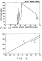
- the concentration of the developing solution changes as shown in FIG. 10 (exhibiting the relationship between the deaeration process time and the number of development defects).
- the concentration of the developing solution increases as a result of vaporization of moisture components, the resultant wiring is obtained with an excessively narrow width. This is a kind of defects. Therefore, it is desirable that the deaeration process time be shorter than 24 hours. However, the deaeration time of the developing solution needs to be longer than 10 minutes because if the deaeration time is shorter than 10 minutes, the deaeration will not be sufficiently performed.
- the pressure of one side portion of the gas-liquid separation membrane is preferably set at 25 to 410 Torr (-350 mmHg to -735 mmHg), and more preferably, 110 to 260 Torr (-500 mmHg to -650 mmHg).
- TMAH tetramethylammonium hydroxide
- the inner pressure of the deaeration chamber be reduced further to the range from 110 to 260 Torr (-500 mmHg to -650 mmHg).
- liquid component of the developing solution includes a gas dissolved in the processing solution and a gas involved in the form of air bubbles.
- a characteristic line Q of measured values approximates a characteristic line P of theoretical values.
- the carrier gas pressure (atm) is directly proportional to the concentration of the nitrogen dissolved in the developing solution.
- the carrier gas falls preferably within the range from 0.5 to 3 kg/cm 2 , and more preferably, from 0.5 to 1.5 kg/cm 2 . This is because if the carrier-gas pressure exceeds 3 kg/cm 2 , the dissolution amount of the gas in the developing solution will be excessively large and instruments attached to the developing-solution supply line will be easily broken. If the carrier gas pressure is smaller than 1.5 kg/cm 2 , the concentration of dissolved nitrogen will be lower than 25 ppm. On the other hand, if the carrier gas pressure is lower than 0.5 kg/cm 2 , the necessary amount of the developing solution will not be supplied. The necessary amount used herein is, for example, about 1.6 little/min. when the nozzle shown in FIGs. 5 and 6, and a wafer of 8-inch diameter are used. It should be noted that the amount of the developing solution consumed per wafer of 8-inch is from 40 to 60 cc.
- the resist processing system according to the present invention comprises:
- the trap tank preferably comprises
- the trap tank further comprises
- the controller controls the deaeration means on the basis of the detection data obtained from the aforementioned two pressure sensors and a liquid surface detection sensor.
- the inner pressure of the deaeration chamber is set at a saturated vapor pressure or less, thereby separating and removing the gaseous component contained in the processing solution without excessively removing the liquid component.
- the controller is preferred to comprise a display portion for displaying the detection data and an alarm portion for giving an alarm when abnormal data (value out of the predetermined range) is presented.
- the alarm draws attention of a worker and let him watch the display portion, so that he knows that an abnormal change occurs in the developing solution.
- the abnormality can be overcome.
- the substrate can be processed constantly without a substantial change in the concentration of the developing solution and without process differences between substrates.
- a developing solution 2 is stored in a main tank 1.
- a gas bomb 3 containing a nitrogen gas is connected via a line 4.
- the line 4 is provided with a pressure control valve 3a.
- An end portion of a line 5 is immersed in the developing solution 2 of the main tank 1.
- the tank 1 has an inner diameter of 20-25 cm and a height of about 50-60 cm.
- the middle of the line 5 is provided with an intermediate tank 6.
- electrostatic-capacity sensors namely a limit sensor 6a and an empty sensor 6b
- Each of the sensors 6a and 6b is connected to an input side of a controller 40, separately.
- the controller 40 operates the pressure control valve 3a on the basis of the detection data so that the surface level of the developing solution 2 stored in the intermediate tank 6 falls within an appropriate range.
- the developing solution 2 is pressurized and sent out to a nozzle 12 through lines 5, 5a and 5b. It is preferable that the pressure of the carrier gas fall within the range of 0.5 to 3 kg/cm 2 .
- the line 5 is branched downstream of the intermediate tank 6 into two lines 5a and 5b and merges at a nozzle 12.
- the first branched line 5a is provided with a flow meter 7a, a filter 8a, a water jacket 9a, a developing-solution deaeration apparatus 10a, and an air-operation valve 11a in that order from the upstream end.
- the second branched line 5b is provided with a flow meter 7b, a filter 8b, a water jacket 9b, a developing-solution deaeration apparatus 10b, and an air-operation valve 11b in that order from the upstream end.
- the filters 8a and 8b are desirably provided at lines 5a and 5b as far upstream as possible.
- the water jackets 9a and 9b may be positioned interchangeably with the developing solution deaeration apparatuses 10a and 10b.
- the developing-solution deaeration apparatuses 10a and 10b are connected to a controller 40.
- the controller 40 controls the operation of the developing-solution deaeration apparatuses 10a and 10b to sufficiently remove the gaseous component from the developing solution without significantly changing the concentration of the developing solution 2.
- the developing process portion 13 comprises a spin chuck 14, a motor 15 and a cup 16.
- the spin chuck 14 is variably rotated by a motor 15 and has a vacuum adsorption mechanism (not shown) for holding a wafer W by adsorption.
- the cup 16 houses the spin chuck 14 and has a drain passage 13a for discharging waste liquid, such as used developing solution.
- the filters 8a and 8b During the passage of the developing solution 2 through the branched lines 5a and 5b, impurities and foreign matters are removed by the filters 8a and 8b, while the flow rate of the developing solution 2 is controlled by the flow-meters 7a and 7b. Since temperature-controlled water is circulated through the water jackets 9a and 9b, the temperature of the developing solution 2 passing through the branched lines 5a and 5b is controlled. After the temperature is adjusted, the developing solutions 2 is introduced into the developing-solution deaeration apparatuses (deaeration mechanism) 10a and 10b, to remove a gaseous component.
- deaeration apparatuses deaeration mechanism
- vacuum evacuation lines 51, 52, 53 and 54 of the developing-solution deaeration apparatus 10a (10b) are provided with a trap tank 21 and an ejector 22.
- the trap tank 21 is communicated with the airtight vessel 61 of the developing-solution deaeration apparatus 10a (10b) through a line 51.
- the trap tank 21 is a vessel for receiving the developing solution 2 leaking from the developing-solution deaeration apparatus 10a through the line 51 during the deaeration operation.
- the bottom of the trap tank 21 is provided with a drain line 57.
- the trap tank 21 is communicated with the ejector 22 through the line 52.
- the line 52 is provided with a stop valve 24 and a solenoid valve 25 in that order when viewed from the side of the trap tank 21.
- the ejector 22 is provided with a line 54 which serves for a different system from the system involving the trap tank 21.
- the line 54 is communicated with an air pump 59.
- the line 54 is provided with a regulator 26 for controlling a flow rate of a supplied air, and a solenoid valve 27.
- a gauge 28 is provided between the regulator 26 and the solenoid valve 27.
- the gauge 28 is connected to the input side of the controller 40.
- the developing-solution deaeration apparatus 10a comprises an airtight vessel (deaeration chamber) 61, an inlet 62, an outlet 63, and a gas-liquid separation element 64.
- the developing-solution deaeration apparatuses 10a and 10b are substantially the same as that disclosed in the United State Patent Application No. 08/579,845.
- a vacuum evacuation line 51 is connected to evacuate the chamber 61.
- the inlet 62 and the outlet 63 are connected to developing solution supply lines 5a (5b).
- the chamber 61 of each of the developing solution deaeration apparatuses 10a and 10b is provided with a vacuum switch 29.
- the vacuum switch 29 is provided with a gauge 29a.
- the gauge 29a is connected to the input side of the controller 40.
- the controller 40 has two output portions which are connected to a display section 41 and an alarm unit 42, separately.
- the controller 40 directs the display section 41 to indicate the abnormal state and direct the alarm unit 42 to give an alarm.
- the controller 40 controls the operation of a regulator 26 and solenoid valves 25 and 27, individually.
- a gas-liquid separation element 64 is provided between the inlet 62 and the outlet 63.
- the developing solution 2 is introduced into the gas-liquid separation element 64 from the inlet 62 through the line 5a (5b).
- the developing solution 2 passes through the gas-liquid separation element 64, goes out from the outlet 63, and is supplied to the nozzle 12 through lines 5a (5b).
- the gas-liquid separation element 64 is formed of a bundle of capillaries made of a porous film, non-porous film, and a composite film.
- a porous film a porous thin film made of polytetrafluoroethylene (PTFE) or a polyolefin-series resin is used.
- a non-porous thin film made of a tetrafluoroethylene ⁇ hexafluoropropylene copolymer (FEP), a tetrafluoroethylene ⁇ perfluoroalkylvinyl ether copolymer (PFA), or polytetrafluoroethylene (PTFE) is used.
- the composite film is a film formed by combining the porous film and the non-porous film.
- the membrane 64a of the gas-liquid separation element 64 has a function of permeating only gaseous component 2a contained in the developing solution 2.
- gaseous component 2a permeable through the membrane 64a include a nitrogen gas molecule, oxygen gas molecule, hydrogen gas molecule, dioxide gas molecular, argon gas molecule, and the like.
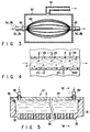
- the nozzle 12 has a developing-solution storing chamber 33 defined by a side wall 31 and a bottom wall 32. An upper opening of the storing chamber 33 is blocked with a covering member 34. The portion between the covering member 34 and the side wall 31 is sealed with a packing 35. Two developing solution supply pipes 37 are provided separately to the covering member 34. The developing solution 2 sent through the lines 5a and 5b is supplied to the developing-solution storing chamber 33 (through two supply pipes 37) and stored therein. In the bottom wall 32, a plurality of liquid expelling holes 38 are formed in the longitudinal direction. The developing solution 2 is supplied from the liquid expelling hole 38 onto the wafer W. The horizontal length of the nozzle 12 is almost equal to the diameter of the wafer W.
- the practical operation procedure is as follows: First, a N 2 gas serving as a pressurized gas is introduced into the tank 1 through the line 4. The developing solution 2 stored in the tank 1 is sent out to the supply line. During this operation, air-operation valves 11a and 11b are closed.
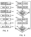
- step S1 When the developing solution 2 is supplied to the developing-solution deaeration apparatuses 10a and 10b, the deaeration of the developing solution 2 is performed at a pressure ranging from 110 to 260 Torr (-500 mmHg to -650 mmHg) just for about 240 seconds (step S1). Details on the deaeration process S1 will be described later with reference to the flow-chart shown in FIG. 9.
- a resist is coated onto the wafer W in a resist coating apparatus (not shown).
- the coated resist is exposed to light in the light-exposure apparatus (not shown).
- the wafer is loaded into the developing unit and mounted on the spin-chuck 14 (step S2).
- the air operation valves 11a and 11b are opened. After the developing solution 2, present in the supply lines 5a and 5b between the developing-solution deaeration apparatuses 10a and 10b and the nozzle, is completely discharged, the deaerated developing solution is newly supplied from the developing-solution deaeration apparatuses 10a and 10b to the supply lines 5a and 5b. In this way, the developing solution to be expelled to the substrate W from the nozzle 12, is replaced with the deaerated developing solution (Step S 3).
- the total amount of 100 cc (sum of the developing solution in lines 5a and 5b) is dispensed (referred to as "dummy-dispense").
- the deaerated developing solution is supplied to the lines 5a and 5b as well as to the nozzle 12. Thereafter, the air operation valves 11a and 11b are closed.
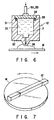
- the nozzle 12 is positioned above in the center of the wafer W. Then, the nozzle 12 is positioned as shown in FIG. 6 by moving up and down relative to the wafer. Thereafter, air operation valves (11a, 11b) are opened to allow the deaerated developing solution to expel from the liquid expelling hole 38. In this manner, the liquid film of the deaerated developing solution is formed between the wafer W surface and the nozzle 12. It is preferred that the expelling amount of the developing solution be smaller than the deaerated developing solution. Conversely, the amount of the developing solution is preferably larger than the expelling amount per time unit (amount per wafer).
- Step, S4 the wafer W is rotated by 180° by means of the motor 15 (Step, S4).
- the developing solution is spread by the rotation of the wafer W, forming a liquid film of the deaerated developing solution on the surface of the wafer W.
- the deaerated developing solution is delivered uniformly over the resist film which has been formed on the wafer W.
- the air-operation valves (11a, 11b) are closed. Since the coated resist is sufficiently exposed to the deaerated developing solution, the coated resist is uniformly developed (Step, S5). In the developing step S5, since deaeration is performed under conditions in which the concentration of the developing solution is not significantly changed, development defects do not occur.
- the dummy dispense be preferably performed before initiation of the processing and at predetermined intervals (30 minutes) for cleaning the supply lines (5, 5a, 5b).
- the amount of the dummy dispense is preferably 100-200 cc, which is larger than the expelling amount per time.
- the amount of the dummy dispense is set to 150 cc, which corresponding to an overall amount of the expelling amount (50 cc) at normal operation and a deaeration amount (100 cc).
- the wafer W is rinsed with pure water while being rotated at high speed (Step, S6). After rinse, the wafer W is unloaded from the developing unit (Step, S7).
- the controller 40 monitors the surface level of the liquid in the trap tank 21 by use of the liquid surface detecting sensor 23. When the liquid surface reaches a preset level, the controller 40 closes the solenoid value 25, thereby terminating the vacuum operation of the chamber 61 through lines 51 to 53.
- the controller 40 opens a valve 57a to discharge the liquid of the trap tank 21 to the drain line 57.
- the controller 40 further opens the solenoid valves 25 and 27 to drive the ejector 22. In this way, the deaeration of the developing solution is started again.
- the vacuum evacuation line 51 Since the vacuum evacuation line 51 is communicated with the drain line 57 of the trap tank 21, leakage of the liquid component can be discharged from the trap tank 21 through the drain line 57. Therefore, even if TMAH (tetramethylammonium hydroxide) acting as an active agent of the developing solution leaks in the vacuum evacuation line 51, the leakage will not affect the vacuum evacuating means (22, 26, 27, 28, 59). The evacuation capacity will not decrease.
- TMAH tetramethylammonium hydroxide
- the vacuum evacuation line 53 positioned downstream of the deaeration apparatus is connected directly to a suction side of a vacuum pump 30. Since the chamber 61 is evacuated directly by the vacuum pump 30 via the vacuum evacuation lines (51 to 53) in the deaeration apparatus, the evacuation capacity will increase. Furthermore, the since the deaeration apparatus is equipped with the trap tank 21 for preventing the vacuum pump 30 from sucking the liquid component leakage, the evacuation capacity will not decrease.
- High-resolution resists coated on 8-inch wafers W were actually developed by using the developing solution deaerated by the method of the present invention, and the developing solution deaerated by a conventional method. Both the resists were compared for development defects. The former resist improves on the latter by 70 % or more, with respect to the defects.
- a stream type nozzle 81 (shown in FIG. 15) or a multi-type nozzle 82 (shown in FIG. 16) formed of a main nozzle provided with a plurality of nozzles 83 may be used.
- the nozzles 81 and 82 are moved from one side portion to the other side in a scanning fashion while the wafer W is being rotated.
- the developing solution 2 is supplied to the wafer W by the stream type nozzle 81 and the multi-type nozzle 82 as follows: First, a N 2 gas is introduced into the tank 1 through the line 4, thereby sending out the developing solution 2 from the tank 1 to the supply line 5. Thereafter, both operation valves 11a and 11b are closed.
- the developing solution 2 is deaerated in the developing-solution deaeration apparatuses 10a and 10b at a saturated vapor pressure or less, for example, 25-410 Torr (-350 mmHg to -735 mmHg) for just 240 seconds.
- the deaerated developing solution is newly supplied in place of the discharged solution.
- the replacement of the developing solution is made by the dummy-dispense of the developing solution (which is attained by opening the air-operation valves 11a and 11b) present in the supply lines (5a, 5b) between the developing-solution deaeration apparatuses (10a, 10b) and a nozzle (81 or 82).
- the air operation valves 11a and 11b are closed.
- the nozzle (81 or 82) is positioned at a distance from the wafer W. After the air operation valves 11a and 11b are opened, the developing solution is expelled from the nozzle (81 or 82) onto the center of the wafer. The wafer W is allowed to rotate while the developing solution is expelled out. The nozzle (81 or 82) is reciprocally moved relative to the wafer W. It is preferable that the expelling amount of the developing solution be smaller than that of the deaerated solution. Conversely, the amount of the developing solution to be deaerated is preferably larger than the expelling amount per time unit.
- a semiconductor wafer is used.
- the present invention is not limited to the semiconductor wafer and an LCD substrate may also be used.
- the resist processing method of the present invention is one performed by supplying a processing solution on the surface of a substrate. Since the process solution employed in the present invention is deaerated within a saturated pressure of the processing solution for at least 15 seconds, the gaseous component contained in the processing solution can be sufficiently removed. Hence, the resist can be processed without defects.
Landscapes
- Physics & Mathematics (AREA)
- General Physics & Mathematics (AREA)
- Engineering & Computer Science (AREA)
- Condensed Matter Physics & Semiconductors (AREA)
- Manufacturing & Machinery (AREA)
- Computer Hardware Design (AREA)
- Microelectronics & Electronic Packaging (AREA)
- Power Engineering (AREA)
- Exposure Of Semiconductors, Excluding Electron Or Ion Beam Exposure (AREA)
- Photosensitive Polymer And Photoresist Processing (AREA)
- Degasification And Air Bubble Elimination (AREA)
Applications Claiming Priority (9)
| Application Number | Priority Date | Filing Date | Title |
|---|---|---|---|
| JP24349396 | 1996-09-13 | ||
| JP243493/96 | 1996-09-13 | ||
| JP24349296A JP3283190B2 (ja) | 1996-09-13 | 1996-09-13 | レジスト処理装置及びレジスト処理方法 |
| JP243492/96 | 1996-09-13 | ||
| JP24349396 | 1996-09-13 | ||
| JP24349296 | 1996-09-13 | ||
| JP22821797A JP3290385B2 (ja) | 1996-09-13 | 1997-08-25 | レジスト処理方法及びレジスト処理装置 |
| JP22821797 | 1997-08-25 | ||
| JP228217/97 | 1997-08-25 |
Publications (2)
| Publication Number | Publication Date |
|---|---|
| EP0829767A1 true EP0829767A1 (de) | 1998-03-18 |
| EP0829767B1 EP0829767B1 (de) | 2002-06-12 |
Family
ID=27331374
Family Applications (1)
| Application Number | Title | Priority Date | Filing Date |
|---|---|---|---|
| EP97115936A Expired - Lifetime EP0829767B1 (de) | 1996-09-13 | 1997-09-12 | Verfahren und Vorrichtung zur Behandlung eines Photoresists |
Country Status (5)
| Country | Link |
|---|---|
| US (2) | US5866307A (de) |
| EP (1) | EP0829767B1 (de) |
| KR (1) | KR100379648B1 (de) |
| DE (1) | DE69713232T2 (de) |
| TW (1) | TW535216B (de) |
Cited By (6)
| Publication number | Priority date | Publication date | Assignee | Title |
|---|---|---|---|---|
| WO2000016163A2 (en) * | 1998-09-17 | 2000-03-23 | Silicon Valley Group, Inc. | Method and apparatus for developing photoresist patterns |
| US6585430B2 (en) | 2000-05-09 | 2003-07-01 | Tokyo Electron Limited | System and method for coating and developing |
| US6689215B2 (en) | 1998-09-17 | 2004-02-10 | Asml Holdings, N.V. | Method and apparatus for mitigating cross-contamination between liquid dispensing jets in close proximity to a surface |
| WO2004036629A1 (en) * | 2002-10-15 | 2004-04-29 | Fsi International, Inc. | Spin-coating methods and apparatuses for spin-coating, including pressure sensor |
| US6746826B1 (en) | 2000-07-25 | 2004-06-08 | Asml Holding N.V. | Method for an improved developing process in wafer photolithography |
| US7404681B1 (en) | 2000-05-31 | 2008-07-29 | Fsi International, Inc. | Coating methods and apparatus for coating |
Families Citing this family (25)
| Publication number | Priority date | Publication date | Assignee | Title |
|---|---|---|---|---|
| GB2342714B (en) * | 1998-10-13 | 2003-04-16 | Memco Ltd | Apparatus for reducing power consumption in a lift door protection system |
| JP3616275B2 (ja) | 1999-05-31 | 2005-02-02 | 東京エレクトロン株式会社 | 液処理装置、それに用いる処理液供給ノズル、および液処理方法 |
| US6238109B1 (en) * | 1999-07-02 | 2001-05-29 | Tokyo Electron Limited | Processing solution supply apparatus |
| KR100877472B1 (ko) * | 2002-01-22 | 2009-01-07 | 도쿄엘렉트론가부시키가이샤 | 기판의 처리방법 및 기판의 처리장치 |
| AU2003234811A1 (en) * | 2002-06-07 | 2003-12-22 | Tokyo Electron Limited | Substrate processing device, substrate processing method, and developing device |
| US20050178322A1 (en) * | 2004-02-17 | 2005-08-18 | Nguyen Andrew P. | Liquid trap for a vacuum line |
| US7651306B2 (en) * | 2004-12-22 | 2010-01-26 | Applied Materials, Inc. | Cartesian robot cluster tool architecture |
| US7819079B2 (en) * | 2004-12-22 | 2010-10-26 | Applied Materials, Inc. | Cartesian cluster tool configuration for lithography type processes |
| US20060130767A1 (en) * | 2004-12-22 | 2006-06-22 | Applied Materials, Inc. | Purged vacuum chuck with proximity pins |
| US7699021B2 (en) * | 2004-12-22 | 2010-04-20 | Sokudo Co., Ltd. | Cluster tool substrate throughput optimization |
| US20060182535A1 (en) * | 2004-12-22 | 2006-08-17 | Mike Rice | Cartesian robot design |
| US7798764B2 (en) * | 2005-12-22 | 2010-09-21 | Applied Materials, Inc. | Substrate processing sequence in a cartesian robot cluster tool |
| US20060241813A1 (en) * | 2005-04-22 | 2006-10-26 | Applied Materials, Inc. | Optimized cluster tool transfer process and collision avoidance design |
| JP4986566B2 (ja) | 2005-10-14 | 2012-07-25 | 大日本スクリーン製造株式会社 | 基板処理方法および基板処理装置 |
| JP2008091533A (ja) * | 2006-09-29 | 2008-04-17 | Toshiba Corp | 薬液の酸化防止装置及び薬液の酸化防止方法 |
| KR100817297B1 (ko) | 2007-04-23 | 2008-03-27 | (주)에스아이엔지니어링 | 차압용 멀티센서를 이용한 레벨 검출 장치 |
| JP6300139B2 (ja) * | 2012-05-15 | 2018-03-28 | 株式会社Screenホールディングス | 基板処理方法および基板処理システム |
| CN103197694B (zh) * | 2013-02-25 | 2016-05-25 | 京东方科技集团股份有限公司 | 流体自动定量供给的控制方法及系统 |
| US9605346B2 (en) * | 2014-03-28 | 2017-03-28 | Lam Research Corporation | Systems and methods for pressure-based liquid flow control |
| US11970772B2 (en) | 2014-08-22 | 2024-04-30 | Lam Research Corporation | Dynamic precursor dosing for atomic layer deposition |
| US10094018B2 (en) | 2014-10-16 | 2018-10-09 | Lam Research Corporation | Dynamic precursor dosing for atomic layer deposition |
| US11072860B2 (en) | 2014-08-22 | 2021-07-27 | Lam Research Corporation | Fill on demand ampoule refill |
| JP6905902B2 (ja) * | 2017-09-11 | 2021-07-21 | 東京エレクトロン株式会社 | 処理液供給装置 |
| KR102572629B1 (ko) * | 2020-09-10 | 2023-08-31 | 세메스 주식회사 | 탈기 장치, 기판 처리 장치 및 처리액 탈기 방법 |
| KR20220067399A (ko) * | 2020-11-17 | 2022-05-24 | 현대자동차주식회사 | 이차전지 코팅 시스템 및 그 방법 |
Citations (5)
| Publication number | Priority date | Publication date | Assignee | Title |
|---|---|---|---|---|
| US5374312A (en) * | 1991-01-23 | 1994-12-20 | Tokyo Electron Limited | Liquid coating system |
| JPH07283184A (ja) * | 1994-04-08 | 1995-10-27 | Tokyo Electron Ltd | 処理装置 |
| JPH08153675A (ja) * | 1994-11-28 | 1996-06-11 | Dainippon Screen Mfg Co Ltd | 基板への処理液供給装置 |
| JPH097936A (ja) * | 1994-12-27 | 1997-01-10 | Tokyo Electron Ltd | レジスト処理装置およびレジスト処理方法 |
| DE19540010A1 (de) * | 1995-07-26 | 1997-01-30 | Samsung Electronics Co Ltd | Anlage und Verfahren zur Halbleiterbauelementherstellung |
Family Cites Families (3)
| Publication number | Priority date | Publication date | Assignee | Title |
|---|---|---|---|---|
| JP2972970B2 (ja) * | 1992-04-24 | 1999-11-08 | 東京エレクトロン株式会社 | 処理装置 |
| JPH07283193A (ja) * | 1994-04-12 | 1995-10-27 | Nippon Steel Corp | 洗浄液乾燥装置 |
| US5618348A (en) * | 1995-01-27 | 1997-04-08 | Dainippon Screen Mfg. Co., Ltd. | Air elimination system |
-
1997
- 1997-09-08 TW TW086113146A patent/TW535216B/zh not_active IP Right Cessation
- 1997-09-11 US US08/927,418 patent/US5866307A/en not_active Expired - Lifetime
- 1997-09-12 DE DE69713232T patent/DE69713232T2/de not_active Expired - Fee Related
- 1997-09-12 KR KR1019970047117A patent/KR100379648B1/ko not_active IP Right Cessation
- 1997-09-12 EP EP97115936A patent/EP0829767B1/de not_active Expired - Lifetime
-
1998
- 1998-10-21 US US09/175,963 patent/US6217657B1/en not_active Expired - Lifetime
Patent Citations (5)
| Publication number | Priority date | Publication date | Assignee | Title |
|---|---|---|---|---|
| US5374312A (en) * | 1991-01-23 | 1994-12-20 | Tokyo Electron Limited | Liquid coating system |
| JPH07283184A (ja) * | 1994-04-08 | 1995-10-27 | Tokyo Electron Ltd | 処理装置 |
| JPH08153675A (ja) * | 1994-11-28 | 1996-06-11 | Dainippon Screen Mfg Co Ltd | 基板への処理液供給装置 |
| JPH097936A (ja) * | 1994-12-27 | 1997-01-10 | Tokyo Electron Ltd | レジスト処理装置およびレジスト処理方法 |
| DE19540010A1 (de) * | 1995-07-26 | 1997-01-30 | Samsung Electronics Co Ltd | Anlage und Verfahren zur Halbleiterbauelementherstellung |
Non-Patent Citations (3)
| Title |
|---|
| PATENT ABSTRACTS OF JAPAN vol. 96, no. 10 31 October 1996 (1996-10-31) * |
| PATENT ABSTRACTS OF JAPAN vol. 96, no. 2 29 February 1996 (1996-02-29) * |
| PATENT ABSTRACTS OF JAPAN vol. 97, no. 5 30 May 1997 (1997-05-30) * |
Cited By (13)
| Publication number | Priority date | Publication date | Assignee | Title |
|---|---|---|---|---|
| US7208262B2 (en) | 1998-09-17 | 2007-04-24 | Asml Holdings N.V. | Yield and line width performance for liquid polymers and other materials |
| WO2000016163A3 (en) * | 1998-09-17 | 2000-09-08 | Silicon Valley Group | Method and apparatus for developing photoresist patterns |
| US6248171B1 (en) | 1998-09-17 | 2001-06-19 | Silicon Valley Group, Inc. | Yield and line width performance for liquid polymers and other materials |
| WO2000016163A2 (en) * | 1998-09-17 | 2000-03-23 | Silicon Valley Group, Inc. | Method and apparatus for developing photoresist patterns |
| US6669779B2 (en) | 1998-09-17 | 2003-12-30 | Asml Holding N.V. | Yield and line width performance for liquid polymers and other materials |
| US6689215B2 (en) | 1998-09-17 | 2004-02-10 | Asml Holdings, N.V. | Method and apparatus for mitigating cross-contamination between liquid dispensing jets in close proximity to a surface |
| US7625692B2 (en) | 1998-09-17 | 2009-12-01 | Asml Holding N.V. | Yield and line width performance for liquid polymers and other materials |
| US7255975B2 (en) | 1998-09-17 | 2007-08-14 | Asml Holding N.V. | Yield and line width performance for liquid polymers and other materials |
| KR100560180B1 (ko) * | 1998-09-17 | 2006-03-13 | 실리콘 밸리 그룹, 인크. | 액체 중합체 및 그 밖의 재료의 수율과 선폭 성능 개선을 위한 장치 |
| US6585430B2 (en) | 2000-05-09 | 2003-07-01 | Tokyo Electron Limited | System and method for coating and developing |
| US7404681B1 (en) | 2000-05-31 | 2008-07-29 | Fsi International, Inc. | Coating methods and apparatus for coating |
| US6746826B1 (en) | 2000-07-25 | 2004-06-08 | Asml Holding N.V. | Method for an improved developing process in wafer photolithography |
| WO2004036629A1 (en) * | 2002-10-15 | 2004-04-29 | Fsi International, Inc. | Spin-coating methods and apparatuses for spin-coating, including pressure sensor |
Also Published As
| Publication number | Publication date |
|---|---|
| US5866307A (en) | 1999-02-02 |
| EP0829767B1 (de) | 2002-06-12 |
| KR100379648B1 (ko) | 2003-08-02 |
| DE69713232T2 (de) | 2002-11-14 |
| KR19980024624A (ko) | 1998-07-06 |
| DE69713232D1 (de) | 2002-07-18 |
| US6217657B1 (en) | 2001-04-17 |
| TW535216B (en) | 2003-06-01 |
Similar Documents
| Publication | Publication Date | Title |
|---|---|---|
| US5866307A (en) | Resist processing method and resist processing system | |
| KR101907351B1 (ko) | 액 처리 방법 및 필터 내의 기체의 제거 장치 | |
| US7685963B2 (en) | Method of and apparatus for dispensing photoresist in manufacturing semiconductor devices or the like | |
| US6193783B1 (en) | Apparatus and method for supplying a process solution | |
| KR100196047B1 (ko) | 레지스트 처리장치 및 레지스트 처리방법 | |
| EP0598424A2 (de) | Vorrichtung zur Entfernung von gelösten Gasen aus einer Flüssigkeit | |
| EP1765674A2 (de) | Zusammenklappbarer fluidbehälter | |
| JP2000173902A (ja) | 基板処理装置 | |
| JP2009166007A (ja) | 塗布液供給装置 | |
| EP0851301B1 (de) | Entwicklungsflüssigkeitsversorgungsvorrichtung | |
| JP3290385B2 (ja) | レジスト処理方法及びレジスト処理装置 | |
| JPH097936A (ja) | レジスト処理装置およびレジスト処理方法 | |
| KR100780936B1 (ko) | 화학용액 내에 포함된 기포를 제거하기 위한 기포제거장치및 이를 이용한 기포제거방법 | |
| JP3283190B2 (ja) | レジスト処理装置及びレジスト処理方法 | |
| JPH04122403A (ja) | 液体供給装置及び脱泡方法 | |
| JP3150690B2 (ja) | 薬液処理装置 | |
| JP3283251B2 (ja) | レジスト処理装置 | |
| JP3347929B2 (ja) | 処理液供給装置 | |
| JP3206745B2 (ja) | 液供給装置 | |
| JPH10128307A (ja) | 膜脱気装置 | |
| JP2813197B2 (ja) | 処理液供給装置 | |
| JPH09150009A (ja) | 処理液供給装置 | |
| JPH10156104A (ja) | 膜脱気装置 | |
| JP2000068197A (ja) | 気泡発生防止兼用気泡除去装置 | |
| JPH05289036A (ja) | 脱気装置を組込んだ液晶供給装置とその運転方法 |
Legal Events
| Date | Code | Title | Description |
|---|---|---|---|
| PUAI | Public reference made under article 153(3) epc to a published international application that has entered the european phase |
Free format text: ORIGINAL CODE: 0009012 |
|
| 17P | Request for examination filed |
Effective date: 19970912 |
|
| AK | Designated contracting states |
Kind code of ref document: A1 Designated state(s): DE FR GB |
|
| AKX | Designation fees paid |
Free format text: DE FR GB |
|
| RBV | Designated contracting states (corrected) |
Designated state(s): DE FR GB |
|
| 17Q | First examination report despatched |
Effective date: 19990226 |
|
| GRAG | Despatch of communication of intention to grant |
Free format text: ORIGINAL CODE: EPIDOS AGRA |
|
| GRAG | Despatch of communication of intention to grant |
Free format text: ORIGINAL CODE: EPIDOS AGRA |
|
| GRAH | Despatch of communication of intention to grant a patent |
Free format text: ORIGINAL CODE: EPIDOS IGRA |
|
| GRAH | Despatch of communication of intention to grant a patent |
Free format text: ORIGINAL CODE: EPIDOS IGRA |
|
| GRAA | (expected) grant |
Free format text: ORIGINAL CODE: 0009210 |
|
| RIN1 | Information on inventor provided before grant (corrected) |
Inventor name: HASEBE, KEIZO, C/O TOYKO ELECTRON LTD. Inventor name: SEMBA, NORIO, C/O TOYKO ELECTRON LTD. Inventor name: KIBA, YUKIO, C/O TOYKO ELECTRON LTD. |
|
| AK | Designated contracting states |
Kind code of ref document: B1 Designated state(s): DE FR GB |
|
| REG | Reference to a national code |
Ref country code: GB Ref legal event code: FG4D |
|
| REF | Corresponds to: |
Ref document number: 69713232 Country of ref document: DE Date of ref document: 20020718 |
|
| ET | Fr: translation filed | ||
| PLBE | No opposition filed within time limit |
Free format text: ORIGINAL CODE: 0009261 |
|
| STAA | Information on the status of an ep patent application or granted ep patent |
Free format text: STATUS: NO OPPOSITION FILED WITHIN TIME LIMIT |
|
| 26N | No opposition filed |
Effective date: 20030313 |
|
| PGFP | Annual fee paid to national office [announced via postgrant information from national office to epo] |
Ref country code: FR Payment date: 20080915 Year of fee payment: 12 |
|
| PGFP | Annual fee paid to national office [announced via postgrant information from national office to epo] |
Ref country code: GB Payment date: 20080917 Year of fee payment: 12 |
|
| PGFP | Annual fee paid to national office [announced via postgrant information from national office to epo] |
Ref country code: DE Payment date: 20080926 Year of fee payment: 12 |
|
| GBPC | Gb: european patent ceased through non-payment of renewal fee |
Effective date: 20090912 |
|
| REG | Reference to a national code |
Ref country code: FR Ref legal event code: ST Effective date: 20100531 |
|
| PG25 | Lapsed in a contracting state [announced via postgrant information from national office to epo] |
Ref country code: FR Free format text: LAPSE BECAUSE OF NON-PAYMENT OF DUE FEES Effective date: 20090930 Ref country code: DE Free format text: LAPSE BECAUSE OF NON-PAYMENT OF DUE FEES Effective date: 20100401 |
|
| PG25 | Lapsed in a contracting state [announced via postgrant information from national office to epo] |
Ref country code: GB Free format text: LAPSE BECAUSE OF NON-PAYMENT OF DUE FEES Effective date: 20090912 |