EP0827322A2 - Telemetrievorrichtung - Google Patents
Telemetrievorrichtung Download PDFInfo
- Publication number
- EP0827322A2 EP0827322A2 EP97304457A EP97304457A EP0827322A2 EP 0827322 A2 EP0827322 A2 EP 0827322A2 EP 97304457 A EP97304457 A EP 97304457A EP 97304457 A EP97304457 A EP 97304457A EP 0827322 A2 EP0827322 A2 EP 0827322A2
- Authority
- EP
- European Patent Office
- Prior art keywords
- current
- circuit
- constant
- polarity inversion
- voltage
- Prior art date
- Legal status (The legal status is an assumption and is not a legal conclusion. Google has not performed a legal analysis and makes no representation as to the accuracy of the status listed.)
- Granted
Links
Images


Classifications
-
- H—ELECTRICITY
- H04—ELECTRIC COMMUNICATION TECHNIQUE
- H04M—TELEPHONIC COMMUNICATION
- H04M3/00—Automatic or semi-automatic exchanges
- H04M3/22—Arrangements for supervision, monitoring or testing
-
- H—ELECTRICITY
- H04—ELECTRIC COMMUNICATION TECHNIQUE
- H04M—TELEPHONIC COMMUNICATION
- H04M11/00—Telephonic communication systems specially adapted for combination with other electrical systems
- H04M11/002—Telephonic communication systems specially adapted for combination with other electrical systems with telemetering systems
Definitions
- the present invention relates to telemetry apparatus, more particularly but not exclusively, to such apparatus used to detect the signals sent from a telephone exchange in a telecommunications system on the commencement and termination of use of the communication line between the exchange and the subscriber.
- the exchange provides a power supply to activate the telephone in a house via the communication line.
- the exchange inverts the polarity of the voltage applied to the communication line between the exchange and the destination subscriber in order to notify the destination subscriber when use of the communication line therebetween starts and stops.
- telemetry systems may use the telephone network as a convenient method of gathering information periodically.
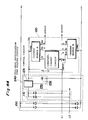
- Fig. 75 is a diagram showing a conventional telemetry system
- Fig. 76 is a block diagram showing the telemetry apparatus.
- the electric power company, the water company, and the gas company each telemeter electric power, water, and gas used in the home via the telephone network. Installed in each house are the power telemetry apparatus, the water telemetry apparatus and the gas telemetry apparatus corresponding to the respective companies.
- the exchange Inverts the voltage polarity of the power supply applied to the communication line between the exchange and the destination consumer.
- each telemetry apparatus has a polarity inversion detection circuit for detecting the polarity inversion, a bell signal detection circuit for detecting the bell signal, and a controlling circuit for controlling the detection circuits and gathering data on electric power, water, and gas from the power meter, the water meter, and the gas meter.
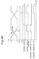
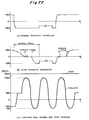
- Fig. 77 is a time chart showing wave shapes, in which Fig. 77 (a) illustrates the wave shape of the polarity inversion of telephone operation (normal polarity inversion); Fig. 77 (b) illustrates the wave shape of the polarity inversion of telemetry (slow polarity inversion); and Fig. 77 (c) illustrates the wave shape of the calling bell signal.
- the calling bell signal follows the normal voltage polarity inversion when a destination subscriber is called for a telephone conversation, but does not follow the slow voltage polarity inversion.
- the telemetry apparatus tries to detect the normal polarity inversion and the calling bell signal, or the slow polarity inversion.
- the telemetry apparatus does not start telemetry but the telephone operates in the conventional manner. On the contrary, if a polarity inversion is found, but no calling bell signal is found, the telemetry apparatus starts telemetry.
- the conventional telemetry apparatus cannot differentiate between a normal polarity inversion and a slow polarity inversion. It relies on the presence or absence of the bell signal to determine whether to initiate telemetry or normal telephone operation. Its inability to distinguish between the polarity inversion signals stems from the technical difficulty that no electric power is provided during the period between the end of the first half of the slow polarity inversion and the start of the second half thereof, because the applied voltage is at ground level during this period.
- the above technology is described in Japanese Laid Open Publication HEI 6-237307.
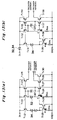
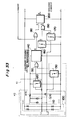
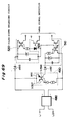
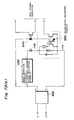
- Fig. 2 illustrates a conventional polarity inversion detection circuit.
- the polarity inversion detection circuit has a rectifier 1 connected to a pair of communication lines L1 and L2.
- the communication line L1 connects to a polarity inversion detection amplification circuit 9 which includes an array of diodes 2 each of which are connected in series, a Zener diode 3 connected to the array of the diodes in parallel, an emitter resistor 4, two transistors Darlington-connected between the resistor 4 and an output terminal of the array of the diodes 2, and a diode 7 and a resistor 8 both of which are connected in series to the collector of a transistor 6, the collector being located at the output side of the transistors 5 and 6.
- the communication line L2 connects to a polarity inversion detection amplification circuit 10 having the same configuration as that of the polarity inversion detection amplification circuit 9.
- a Zener diode 11 Between the output terminal of the array of the diodes 2 in the polarity inversion detection amplification circuit 9 and the output terminal of the array of the diodes 2 in the polarity inversion amplification circuit 10, a Zener diode 11, a resistor 12, a capacitor 13, a resistor 14 and a Zener diode 15 are connected in series in this described order.
- the exchange Inverts the polarity of voltage applied thereto so as to notify the telemetry apparatus of the start and release.
- the polarity inversion on the communication lines L1 and L2 starts and when thereby the voltage between the communication lines L1 and L2 varies, either Zener diode 11 or Zener diode 15 detects the change to turn into a current passing state, and thus a polarity inversion detection trigger current flows in accordance with the charging and discharging of the capacitor 13.
- the polarity inversion detection amplification circuit 9 or the polarity inversion detection amplification circuit 10 amplify the trigger current via the array of diodes 2, the Zener diodes 11 and 15 and the resistors 12 and 14.
- the holding circuit 16 or the holding circuit 17 hold polarity inversion information, with an amplified trigger current, output from the polarity inversion detection amplification circuit 9 or from the polarity inversion detection amplification circuit 10, as a trigger. Also, they output the polarity inversion information to the controlling circuit using an externally attached circuit such as a photo coupler. When it is no longer necessary to hold the polarity inversion information, a reset signal is produced by the controlling circuit so that the information held in the holding circuits 16 and 17 is cleared. Thus, the circuits return to a stand-by state.
- conventional telemetry apparatus detects a polarity inversion on the communication lines L1 and L2 using, for example, the polarity inversion detection circuit shown in Fig. 2.
- the controlling circuit determines which of telemetry or telephone the use of the communication line is directed to, which depends on a bell signal which follows the normal polarity inversion but does not follow the slow polarity inversion.
- conventional bell signal detection circuits For detection of the bell signal, conventional bell signal detection circuits perform a logic OR on the two polarity inversion signals indicating either a start or a release of the use of lines L1, L2, generated by the Zener diodes 11 and 15 shown in Fig. 2, the resistors 12 and 14, the capacitor 13 and the polarity inversion detection amplification circuits 9 and 10, whereby they obtain a stream of short pulses and detect a bell signal based on the stream.
- telemetry apparatus comprising a detecting circuit for detecting deviations from a signal reference value on one or more communication paths within a telemetry system, characterised in that the detecting circuit is arranged to distinguish between signals with different rates of deviation.
- the deviations to be detected may comprise polarity inversions.
- the telemetry apparatus may distinguish the normal polarity inversion, the slow polarity inversion, and the calling bell signal applied to the communication line between the telemetry apparatus and the exchange in a telephone network.
- the invention may comprise edge detection means for detecting one of a rising edge and a falling edge based on predetermined levels of the edges and predetermined periods of the edges characterising each of the signals from the exchange.
- the preferred embodiments of the telemetering apparatuses are principally classified into three parts: detection of the normal polarity inversion, detection of the slow polarity inversion, detection of the bell signal.
- detection of the normal polarity inversion there are a edge detection circuit, a state holding circuit, and a polarity inversion detection circuit, which constitutes a normal polarity inversion circuit.
- detection of the slow polarity inversion in addition to those circuits, there are a polarity inversion detection circuit and a monostable multivibrator, which constitutes a telemetering apparatus to work in response to the slow polarity inversion.
- For detection of the bell signal there is a bell signal detection circuit.
- As an application of detecting the edge there is a high voltage detection circuit.
- the edge detection circuit will be principally described with reference to Figs. 3 ,8, and 9;
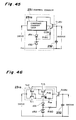
- the slow polarity inversion detection circuit will be principally described with reference to Figs. 33 and 42;
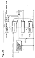
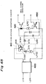
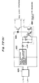
- Fig. 1 is a figure illustrating a polarity inversion detection circuit of the first embodiment according to the present invention.
- the polarity inversion detection circuit is provided in a telemetering apparatus to detect polarity inversions representing a starting or a releasing use of communication line, which are performed by the exchange via the communication line.
- the polarity inversion detection circuit has a full-wave rectifier 20 connected between the communication lines L1 and L2, a first edge detection circuit 30A connected between a negative electrode terminal (-) of the full-wave rectifier 20 and the line L1, and a second edge detection circuit 30B connected between the negative electrode terminal (-) of the full-wave rectifier 20 and the line L2.
- the output sides of the edge detection circuits 30A and 30B are connected to input terminals of a OR circuit 40 respectively.
- the OR circuit 40 is, for example, a wired OR to process output signals of the edge detection circuits 30A and 30B.
- a constant-current on/off typed holding circuit 50 is connected between the positive electrode terminal and negative electrode terminal of the full-wave rectifier 20, moreover.
- the constant-current on/off typed holding circuit 50 has a set input terminal S and a reset input terminal R.
- the output signal of the OR circuit 40 and a reset signal from the controlling circuit are provided to the set inuut terminal S and the reset input terminal R respectively.
- the constant-current on/off holding circuit 50 outputs the result of the polarity inversion detection.
- the structure and the function [I] and the operation [II] of each circuit in the polarity inversion detection circuit shown in Fig. 1 will be separately described below. Further, the effect of the polarity inversion detection circuit shown in Fig. 1 will be described at the following section [III].
- the full-wave rectifier 20 performs full-wave rectification on the currents flowing on the communication lines L1 and L2 to output a voltage in a fixed polarity.
- the full-wave rectifier 20, for example, is made from diodes which is one of the semiconductor rectifying devices which are embedded on four sides of a bridge respectively.
- the opposing two corners of the bridge are connected to the communication lines L1 and L2 respectively, and the other opposing two corners are the positive electrode terminal (+) and the negative electrode terminal (-) respectively.
- Each of the edge detection circuit 30A and 30B detects the releasing signal or the starting signal via the communication lines L1 and L2 respectively to output an edge detection trigger pulse.
- the edge detection circuits 30A and 30B will be described in detail.
- Fig. 3 is a block diagram illustrating the elements of the edge detection circuits 30A and 30B shown in Fig. 1.
- the edge detection circuits 30A and 30B have the same configuration. Each of them has a first constant-current loop 31, a first constant-voltage element 32, a feed back loop 33, and a constant-voltage element 34.
- the constant-current loop 31 allows a constant-current i on to flow in accordance with an applied voltage.
- the first constant-voltage element 32 prevents the current i on from flowing into the constant-current loop 31 when the applied voltage is below V on either, which is performed by restricting the operation of the current loop amplification in the constant-current loop 31 through connection into the current loop 31, or by restricting the amount of the applied voltage of the constant-current loop 31 through connection to the current path of the constant-current loop 31 in serial.
- the feed back loop 33 serves as a feed back circuit for the constant-current loop 31 in order to cause the total current in the whole circuit (including the constant-current loop 31) to be zero by reducing the loop current amplification factor of the whole circuit below 1.
- the constant-voltage element 34 is connected in the feedback loop 33, and stops the feedback operation of the feedback loop 33 when the applied voltage is below V off .
- the combination of the constant-current loop 31, the feedback loop 33 and the constant-voltage elements 32 and 34 composes the constant-current circuit.
- the constant-current i on which flows from the constant-current circuit, is changed into an output current by the two of the current mirror circuits 35 and 36.
- the constant-current loop 31 to which the constant-voltage element 32 and the feedback loop 33 (including the constant-voltage element 34) are attached and the current mirror circuits 35 and 36 are connected between the input terminal, which is connected to a communication line L1 or L2, and the ground.
- Each output terminal of the current mirror circuits 35 and 36 is an output terminal to indicate detection of a pulse edge.
- the constant-voltage element 32 allows conduction and also the feedback loop 33 does not allow feedback operation, the constant current loop 31 is forced into an on-state, thus permitting the current i on to flow.
- the constant-current loop 31 does not work, thereby forbidding the current i on to flow.
- the feedback loop 33 is forced into operation when the constant-voltage element 34 allows conduction.
- the voltage Von of the constant-voltage element and the voltage Voff of the constant-voltage element are set in such a fashion that the latter voltage Voff is larger than the former voltage Von. Consequently, the current i on can flow only when an applied voltage is laid in the range from Von to Voff.
- edge detection circuits 30A and 30B Before describing the specific circuit configuration on the edge detection circuits 30A and 30B, in reference with Fig. 4 through Fig. 6, the edge detection circuits 30 and 40, a liner current mirror circuit used for other circuits shown in this specification, and two kinds of non-linear current amplifiers will be described.
- Fig. 4 (a) through (f) illustrate the linear current mirror circuit, wherein Fig. 4 (a) shows a symbolic representation and Fig. 4 (b) through (f) are its example circuits.
- the linear current mirror circuit has three terminals including: an input terminal I from which a current flows out (in); an output terminal O from which a current flows out (in); and a common terminal COM to which the total amount of currents on the input terminal I and the output terminal O flows in, thereby the Input/Output relation of the circuit is a linear amplification.
- the circuit shown in Fig. 4 (b) has a pair of PNP transistors Tr1 and Tr2 , in which both emitters of them are connected to the common terminal COM. Both bases of the transistors Tr1 and Tr2 are connected to the collector of the transistor Tr1.
- the collector of the transistor Tr1 is the input terminal I while the collector of the transistor Tr2 is the output terminal O.
- the circuit shown in Fig. 4 (c) has the configuration that emitter resistors R1 and R2 are inserted between the emitters of the transistors Tr1 and Tr2 and the common terminal COM shown in Fig. 4 (b) respectively.
- the circuit shown in Fig. 4 (d) has transistors Tr3 and Tr4 added to the circuit shown in Fig. 4 (b).
- the emitter of the transistor Tr3 is connected to the common terminal COM while the collector of the transistor Tr3 is connected to the emitter of the transistor Tr1.
- the emitter of the transistor Tr4 is connected to the common terminal COM while the collector of the transistor Tr4 is connected to the emitter of the transistor Tr2.
- the bases of the transistors Tr3 and Tr4 are connected to the collector of the transistor Tr4.
- the circuit shown in Fig. 4 (e) has the configuration that emitter resistors R3 is inserted between the emitter of the transistor Tr3 and the common terminal COM, and that emitter resistor R4 is inserted between the emitter of the transistor Tr4 and the common terminal COM.
- the circuit shown in Fig. 4 (f) has the configuration that PMOS transistors PTr1 and PTr2 are substituted for the transistors Tr1 and Tr2 shown in Fig. 4 (b) respectively. That is, both the sources of the PMOS transistors PTr1 and PTr2 are connected to the common terminal COM, while both the gates of the PMOS transistors PTr1 and PTr2 are connected to the drain of the transistor Tr1.
- the drain of the PMOS transistor PTr1 is the input terminal I while the drain of the PMPS transistor PTr2 is the output terminal O.
- Each of the circuits shown in Fig. 4 (b) through (e) uses PNP transistors, however, it is also possible to use NPN transistors in place of PNP transistors.
- the circuit shown in Fig. (f) uses PMOS transistors, however, it is also possible to use NMOS transistors in place of PMOS transistors.
- the circuits shown in Fig. 4 (b) through (e) can be replaced with MOS transistors.
- Fig. 5 (a) through (f) illustrate non-linear current amplifiers (constant-current source typed current amplifier), wherein Fig. 5 (a) shows a symbolic representation and Fig. 5 (b) through (f) are its example circuits.
- Each of the non-linear current amplifiers has three terminals including: an input terminal I for a current flowing in (out); an output terminal O for a current flowing in (out); and a common terminal COM in which a total amount of currents of the input terminal I and the output terminal O.
- the non-linear current amplifiers have the maximum current gain at around zero in an input current, and the property that the current gain monotonously decreases toward zero while the input current increases.
- This type of the non-linear current amplifier is referred as a constant-current source typed current amplifier below, since from the combination of it and the linear current mirror circuit shown in Fig. 4 a constant-current circuit can be made.
- the circuit shown in Fig. 5 (b) has a transistor Tr5 in which both its base and collector are connected to a input terminal I, and a transistor Tr6 in which its collector is connected to the output terminal O.
- the emitter of the transistor Tr5 is connected to a common terminal COM while the emitter of the transistor Tr6 is connected to the common terminal COM via a resistor Ron.
- the bases of the transistors Tr5 and Tr6 are connected to the collector of Tr5.
- the circuit shown in Fig. 5 (c) has the configuration in that a diode dl is placed between the emitter of the transistor Tr5 and the common terminal COM shown in Fig. 5 (b).
- the circuit shown in Fig. 5 (d) has the configuration that transistors Tr7 and Tr8 are added to the circuit shown in Fig. 5 (b).
- the emitter of the transistor Tr7 is connected to a common terminal COM while the collector of the transistor Tr7 is connected to the emitter of the transistor Tr5.
- the emitter of the transistor Tr8 is connected to the common terminal COM via a resistor Ron while the collector of the transistor Tr8 is connected to the emitter of the transistor Tr6.
- the bases of the transistor Tr7 and Tr8 are connected to the collector of the transistor Tr8.
- Fig. 5 (e) has the configuration in that a diode dl is inserted between the emitter of the transistor Tr7 and a common terminal COM.
- the circuit shown in Fig. 5 (f) has the configuration in that NMOS transistors NTr1 and NTr2 is substituted for the transistors Tr5 and Tr6 respectively as shown in Fig. 5 (b). That is, the source of the NMOS transistor NTr1 is directly connected to a common terminal COM, and the source of the NMOS transistor NTr2 which has a gate width larger than the gate width of the NMOS transistor NTr1 is connected to the common terminal COM via a resistor Ron.
- NMOS transistor NTr2 The back-gate of NMOS transistor NTr2 is connected to the common terminal COM, and both gates of NMOS transistors NTr1 and Ntr2 are connected to the drain of the transistor NTr1.
- the drain of the NMOS transistor NTr1 is an input terminal I while the drain of the NMOS transistor NTr2 is an output terminal O.
- Each of the circuits shown in Fig. 5 (b) through (e) uses NPN transistors, however, it is also possible to use PNP transistors in place of NPN transistors. Just like the circuit shown in Fig. 5 (b) is replaced with the one shown in Fig. (f), the configurations shown in Fig. 5 (b) through (e) can be created using MOS transistors.
- Fig. 6 (a) through (g) illustrate non-linear current amplifiers (switch typed current amplifiers),wherein Fig. 6 (a) is a symbolic representation and Fig. (b) through (g) are its example circuits.
- non-linear current amplifiers shown in Fig. 6 (a) through (g) have three terminals including: an input terminal I for a current flowing in (out), an output terminal O for a current flowing in (out), and a common terminal COM for a current flowing out (in). They have the minimum current gain at around zero in input current and the property that current gain monotonously increases in accordance with increase of the input current.
- this type of non-linear current amplifier is referred to as a switch typed current amplifier, since the combination of it and the linear current mirror circuit shown in Fig. 4 can make a switch circuit.
- the circuit shown in Fig. 6 (b) has a transistor Tr9 whose base and collector both are connected to an input terminal I and a transistor Tr10 whose collector is connected to an output terminal O.
- the emitter of the transistor Tr9 is connected to a common terminal COM via a resistor Rth while the emitter of the transistor Tr10 is directly connected to the common terminal COM.
- the base of the transistor Tr10 is connected to the collector of the transistor Tr9.
- both the base of a transistor Tr11 and one end of a resistor Rth are connected to an input terminal I.
- the collector of the transistor Tr11 is connected to an output terminal O while both the emitter of the transistor Tr11 and the other end of the resistor Rth is connected to the common terminal COM.
- the circuit shown in Fig. 6 (d) has the configuration in that a diode d2 is inserted between the emitter of the transistor Tr10 and the common terminal COM as shown in Fig. 6 (b).
- the circuit shown in Fig. 6 (e) has the configuration in that transistors Tr12 and Tr13 are added to the circuit shown in Fig. 6 (b).
- the emitter of the transistor Tr12 is connected to a common terminal COM via the resistor Rth while the collector of the transistor Tr12 is connected to the emitter of a transistor Tr9.
- the emitter of a transistor Tr13 is connected to the common terminal COM while the collector of the transistor Tr13 is connected to the emitter of the transistor Tr10. Both bases of the transistors Tr12 and Tr13 are connected to the collector of the transistor Tr13.
- the circuit shown in Fig. 6 (f) has the configuration in that transistors Tr12 and Tr13 are added to the circuit shown in Fig. 6 (d).
- the circuit shown in Fig. 6 (g) has the configuration in that the transistors Tr9 and Tr10 shown in Fig. 6 (b) are replaced with NMOS transistors NTr3 and NTr4 respectively.
- the source of the NMOS transistor NTr3 which has a gate width larger than the gate width of the NMOS transistor NTr4 is connected to a common terminal COM via a resistor Rth while the source of the NMOS transistor NTr4 is directly connected to the common terminal COM.
- Both gates of the transistors NTr3 and NTr4 are connected to the drain of the transistor NTr3.
- the drain of the NMOS transistor NTr3 is an input terminal I while the drain of the NMOS transistor NTr4 is an output terminal O.
- the circuits shown in Fig. 6 (b) through (f) use NPN transistors, however, it is possible to replace each NPN transistor with a PNP transistor or a MOS transistor.
- Fig. 7 illustrates the example configuration of the edge detection circuit shown in Fig. 3, wherein the same elements as the ones in Fig. 3 are attached the same respective reference numerals in Fig. 7.
- the edge detection circuit has a first current mirror circuit M1 which is made from, for example, the linear current mirror circuit shown in Fig. 4 (b), a constant-current source typed current amplifier C1 which is a first non-linear current amplifier, a constant-voltage element 32 which is a Zener diode, and capacitor Cp1.
- the output terminal O of the constant-current source typed current amplifier C1 is connected to an input terminal I
- the output terminal O of the current mirror circuit M1 is connected to the cathode of the constant-voltage element 32
- the anode of the constant-voltage element 32 is connected to the input terminal I of the constant-current source typed current amplifier C1, a current amplification loop is made.
- the circuit in that the cathode and the anode of the constant-voltage element 32 are short-circuited, corresponds to the constant-current loop 31 as shown in Fig. 3.
- the constant-voltage element 32 can also be inserted between the output terminal O of the constant-current source typed current amplifier C1 and the input terminal I of the current mirror circuit M1 so as to have the same effect.
- a capacitor Cp1 is connected between the input and the output terminals of the current mirror circuit M1.
- the edge detection circuit has, other than the constant-current loop 31, a second linear current mirror circuit M2 made from the linear current mirror circuit shown in Fig. 4 (b), a switch typed current amplifier S1 as the second non-linear current amplifier shown in Fig. 6 (b), and a constant-voltage element 34 which is a Zener diode.
- the output terminal O of the current mirror circuit M2 is connected to the cathode of the constant-voltage element 34 while the anode of the constant-voltage element 43 is connected to the input terminal I of the switch typed current amplifier S1.
- the circuit in that the cathode and the anode of the constant-voltage element 34 are short-circuited, corresponds to the feedback loop 33 as shown in Fig. 3.
- the common terminal COM of the current mirror circuit M1 in the constant-current loop 31 is connected to the input terminal I of the current mirror circuit M2 in the feedback loop 33, and the output terminal O of the switch typed current amplifier S1 in the feedback loop 33 is connected to the input terminal I of the constant-current source typed current amplifier C1 in the constant current loop 31.
- the common terminal COM of the current mirror circuit M2 in the feedback loop 33 is connected to the input terminal I of the current mirror circuit 35 while both common terminal COM of the switch typed current amplifier S1 and the common terminal COM of the constant-current source typed current amplifier C1 are connected to the input terminal I of the current-mirror circuit 36.
- the common terminal of the current mirror circuit 36 is connected to the ground terminal GND of the edge detection circuits 30A and 30B while the common terminal COM of the current mirror circuit 35 is connected to the input terminal IN of the edge detection circuits 30A and 30B.
- the output terminal O of the current mirror circuit 35 is connected to the negative output terminal for flowing a current out OUT - while the output terminal O of the current mirror circuit 36 is connected to the positive output terminal for a current flowing in OUT + of the edge detection circuits 30A and 30B.
- the current mirror circuits M1 and M2 are made from, for example, the circuit shown in Fig. 4 (b).
- the switch typed current amplifier S1 is made from the circuit shown in Fig. 6 (b).
- the current mirror circuit 35 has a pair of PNP transistors Tr14 and Tr15 whose emitters are connected to a common terminal COM. Both the collector and the base of the transistor Tr14 are connected to the input terminal I of the current mirror circuit 35 while the collector of the transistor Tr15 is connected to the output terminal OUT- via the output terminal O of the current mirror circuit 35. The base of the transistor Tr15 as well as both the collector and the base of the transistor Tr14 are connected to the input terminal I of the current mirror circuit 35.
- the current mirror circuit 36 has a pair of NPN transistors Tr16 and Tr17 whose respective emitters are connected to a common terminal COM. Both the collector and the base of the transistor Tr16 are connected to the input terminal I of the current mirror circuit 36 while the collector of the transistor Tr17 is connected to the output terminal OUT+ via the output terminal O of the current mirror circuit 36. The base of the transistor Tr17 as well as both the collector and the base of the transistor Trl6 are connected to the input terminal I of the current mirror circuit 36.
- these current mirror circuits 35 and 36 are prepared to output. When either the output current for flowing in or the other output for flowing out is unnecessary, accordingly, either the current mirror circuit 35 or the current mirror circuit 36 can be omitted.
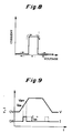
- Fig. 8 illustrates the relation between an applied voltage and an amount of flowing current in the edge detection circuit.
- Fig. 9 illustrates an applied voltage and a current which flows at a transient time of an edge detection.
- the constant-current loop 31 turns on when the voltage V reaches a certain low voltage, whereby the current i on begin to flow in the constant-current loop 31.
- the constant-voltage element 32 prevents the loop current amplification of the constant-current loop 31 (when connected in the constant-voltage loop 31), or keeps the voltage V applied on the constant-current loop 31 such low not to enable it to work (when connected to the constant-current loop 31 in serial). This keeps the constant-current loop 31 non-active. Further, rising of the applied voltage beyond the voltage V on forces a breakdown on the constant-voltage element 32.
- the constant-current loop 31 Upon breakdown of the constant-voltage element 32, the condition that forces the constant-current loop 31 to be held in an off-state is removed. Accordingly, the constant-current loop 31 turns on, whereby the constant-current i on begins to flow. With the breakdown point of the constant-voltage element 34 being set higher than that of the constant-voltage element 32, at this set point the constant-voltage element 34 does not experience any breakdown, namely in cutoff-status.
- the feedback loop 33 cannot implement such a feedback as to allow the current loop 31 to be an off-state.
- a breakdown on the constant-voltage element 34 occurs to start the operation of the feedback loop 33.
- the loop current gain of the constant-current loop 31 including the feedback loop 33 always becomes less than 1, and current decreases little by little into an off-state.
- a current according to the constant-current I on is outputted through the current mirror circuits 35 and 36.
- the current I on flows only during the time between Von of the leading voltage edge of the input pulse and Voff, and thereby a trigger current as an edge detection pulse is obtained.
- the current value I on is decided by a predetermined current value of the constant-current loop 31, and pseudo-differential can be attained without detrimental effects from the magnitude of the velocity dV/dt. 0 ⁇ Von ⁇ Voff ⁇ Vp
- the constant-current loop 31 when the constant-voltage element 32 is short-circuited will be taken in account.
- the current amplification factor the product between current amplification factors of two current amplifiers; hereinafter it is referred to as a loop current amplification factor
- the current on the common terminal COM is also a constant-current which is one-dimensionally decided by the current i on .
- the current i flowing to the constant-current loop 31 is decided by both the band gap voltage according to the ratio of transistor size n and a resistor Ron.
- n The ratio of transistor size of the constant-current source typed current amplifier C1 is denoted by n, the resistance value of resistor is denoted by r on , the current gain of the current mirror circuit M1 is denoted by K, Boltzmann's constant is denoted by k, an electric charge of an electron is denoted by q, an absolute temperature is denoted by T, and an amount of current flowing on the common terminal COM is denoted by i on again.
- i on can be approximated in accordance with the following Expression (3).
- i on (kT/qr on )(1+K)ln(nK)
- the constant-current loop 31 can not make loop-current amplification and stays in an off-state. Therefore, by selecting the breakdown voltage of the constant-voltage element 32, the voltage for starting a current from flowing can be controlled.
- the current mirror circuit M2 When a current flows on the aforementioned current path, the current mirror circuit M2 tries to flow a current, in proportion to the one flowing on the constant-current loop 31, on the path making a trip among the output transistor Tr2 in the current-mirror circuit M2 which is a current path of the feedback loop 33, the constant-voltage element 34 and the input terminal of the switch typed current amplifier S1.
- the current does not flow as long as a breakdown does not occur on the constant-voltage element 34.
- the constant-voltage element 34 controls the voltage for starting a current from flowing.
- the output current of the switch typed current amplifier S1 takes a flowing-in current to the input terminal I of the constant-current source typed current amplifier in the constant-current loop 31. Therefore, the loop current gain of the constant-current loop 31 including the feedback loop 33 is set less than 1, and the constant-current loop 31 works as a loop approaching an off-state. Whether a final current value is zero or approaches a very close to zero can be decided by the switch typed current amplifier S1.
- the current i on flows only within a short period of time from Von through Voff in a leading voltage edge when an input pulse pass the period, and conversely, no current flows at more than Voff. Thereby, a pulse edge can be detected.
- a capacitor Cp1 charging current when an applied voltage V rises forces the constant-current loop 31 into an on-state easier.
- a capacitor Cp1 discharging current when the applied voltage falls prevents the constant-current loop 31 from becoming on.
- a leading edge of the applied voltage can be detected (a current flows), however, a trailing edge of it can not be detected (no current flows).
- the current value is decided by a set-up current value on the constant-current loop 31 as long as the capacity of the capacitor Cp1 is not large, and thus it is not affected by the changing velocity dV / dt on the input pulse.
- the constant-voltage element 32 is prepared in order to set an on-state-starting voltage Von for the constant-current loop 31.
- the same effectiveness can be obtained by connecting it somewhere among the path designated by the current mirror circuit M2, transistors in the current mirror circuits 35 and 36 and the constant-current loop 31, the path in which a current passes at first.
- it is possible to shift both the voltage Von and Voff by connecting the constant-voltage element 32 in series to a transistor in the current mirror circuits 35 and 36 which are places outside of the paths included in the feedback loop 33.
- Fig. 10 is a block diagram showing positions in which the constant-voltage elements 34 and 32 as shown in Fig. 3 are inserted.
- Fig. 10 the current mirror circuit, constant-current source typed current amplifier and the switch typed current amplifier in the edge detection circuits 30A and 30B are represented with symbolic notations illustrated in Fig. 4 (a), Fig. 5 (a) and Fig. 6 (a), however, the current mirror circuits 35 and 36 are omitted.
- the constant-voltage elements 32 and 34 can be inserted into different positions in the edge detection circuit as shown in Fig. 10. Insertion of a constant-voltage element into the place which is referred to as 'PL1' influences the Von. Insertion of it into the place which is referred to as 'PL2' influences the Voff. Insertion of it into both places which are referred to as 'PL1' and 'PL2' influences both of Von and Voff voltages.
- Fig. 11 is a block diagram showing an example of modification of the circuit shown in Fig. 7.
- Several current mirror circuits in the block diagram are replaced with a current mirror circuit.
- the current mirror circuits 35 and 36 are omitted because they are obvious to those skilled in the art.
- Fig. 12 shows an example circuit using MOS transistors for the feedback loop 33 according to Fig. 7.
- the current mirror circuits 35 and 36 are omitted because they are obvious to those skilled in the art.
- the feedback loop 33 should only satisfy that the loop current amplification factor of the constant-current loop 31 is less than 1, and that the dissipation power during standby is zero. Therefore, like the circuit shown in Fig. 12, using the MOS transistors NTr38 and NTr 39 makes the circuit simpler.
- Fig. 13 (a) through (e) show circuits as other example configurations than Fig. 7, and show the constant-current loop 31 which linearly outputs.
- the constant-current source typed current amplifier in the constant-current loop 31 can obtain a linear output like a current mirror circuit by adding transistors for obtaining the linear output.
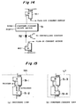
- Fig. 14 is a block diagram illustrating an example configuration according to the constant-current ON/OFF typed holding circuit 50 shown in Fig. 1.
- the constant-current ON/OFF typed holding circuit 50 has a current mirror circuit M11 made from the linear current mirror circuit as shown in Fig. 4, a constant-current ON/OFF switch circuit 51, an output circuit which, for example, is configured with a photo coupler 52 , and a current mirror circuit M12 made from the linear current mirror circuit shown in Fig. 4.
- the common terminal COM in the current mirror circuit M11 is connected to a power supply V+ which comes from the positive electrode terminal of the full-wave rectifier 20.
- the input terminal of the current mirror circuit M11 is connected to a current flowing-in terminal of the constant-current ON/OFF typed current switch 51.
- the current flowing-out terminal of the constant-current ON/OFF switch 51 is connected to the input anode terminal of the photo coupler 52.
- the input cathode terminal of the photo coupler 52 is connected to the input terminal I of the current mirror circuit M12.
- the common terminal of the current mirror circuit M12 is connected to the power supply V- which comes from the negative electrode terminal of the full-wave rectifier 20.
- the constant-current ON/OFF typed switch 51 has a set input terminal S and a reset input terminal R.
- the current mirror circuit M11 has a flowing-out current as its output.
- the current mirror circuit M12 has a flowing-in current as its output.
- the photo coupler 52 outputs to other circuits which have different ground levels. Here, one of either the photo coupler 52 or the current mirror circuit M11 or the current mirror circuit M12 can be omitted when it is unnecessary according to the their following connected circuit..
- the constant-current ON/OFF typed current switch 51 which will be described later in detail, becomes an on-state when a trigger current flows in from a set input terminal S. Thereby, a constant current flows between the current flowing-in terminal and the current flowing-out terminal. Otherwise, the constant-current ON/OFF typed current switch 51 becomes an off-state when a trigger current flows in from a reset input terminal R ,and the constant current becomes zero.
- a constant current i on during on-state and an input threshold current i th are decided independently from each other by a band gap voltage according to the ratio in transistor size and a resistor size, the ratio of the constant current i on during on-state to the input threshold current i th can be kept constant.
- Both the input circuit of the photo coupler 52 and the current mirror circuits M11 and M12 are connected to diodes respectively in forward direction.
- the ON/OFF states on the currents flowing on them are decided in accordance with the state on the constant-current ON/OFF typed switch 51.
- the constant current i on which becomes on and off is transformed to a flowing-out current output signal by the current mirror circuit M11, and is transformed to a flowing-in current output signal, by the current mirror circuit M12. Moreover, in accordance with the constant current i on which becomes on and off, an on-signal and an off-signal are sent to the controlling circuit which has a different ground level through the photo coupler 52.
- Fig. 15 illustrates the constant-current ON/OFF typed current switch shown in Fig. 14.
- the constant-current ON/OFF typed current switch 51 is made from the combination of the switch loop SWL and the constant-current loop ILP shown in Fig. 15.
- the switch loop SWL has a current-mirror circuit 51-1 made from the current mirror circuit shown in Fig. 4 and a switch typed current amplifier 51-2 which is a non-linear current amplifier made from the switch typed amplifier 51-2.
- the input terminal I of the current mirror circuit 51-1 is connected to the output terminal O of the switch typed current amplifier 51-2, and the input terminal the input terminal I of the switch typed current amplifier 51-2 is connected to the output terminal O of the current mirror circuit 51-1.
- the current loop of the switch loop SWL has a current path between common terminals of the current mirror circuit 51-1 and the switch typed current amplifier 51-2. This operates as a switch to control on and off in the circuit by flowing a trigger current either to an input/output connection terminal of the current mirror circuit 51-1 or to the one of the switch typed current amplifier 51-2 and by making the current in the circuit either more than or less than i th .
- the constant-current loop ILP has a current mirror circuit 51-3 which has the same configuration as the current mirror circuit 51-1 and a constant-current source typed current amplifier 51-4 which is equivalent to the non-linear typed current amplifier shown in Fig. 5.
- the output terminal O of the constant-current source typed current amplifier 51-4 is connected to the input terminal I of the current mirror circuit 51-3.
- the output terminal O of the current mirror circuit 51-3 is connected to the input terminal of the constant-current source typed current amplifier 51-4.
- the circuit between common terminals COMs of the constant-current source typed current amplifier 51-4 and the current mirror circuit 51-3 has a constant-current characteristic, as mentioned above in section [1](2)(iii).
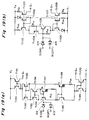
- Fig. 16 and Fig. 17 illustrates the first specific example of the constant-current ON/OFF typed current switch shown in Fig. 14.
- the constant-current ON/OFF typed current switch shown in Fig. 16 has a configuration in that a switch loop SWL is inserted between an input terminal I of a current mirror circuit 51-3 in a constant-current loop ILP and an output terminal O of a constant-current source typed current amplifier 51-4. That is, the input terminal I of the current mirror circuit 51-3 is connected to a common terminal COM of the current mirror circuit 51-1 in the switch loop SWL, and the output terminal O of the constant-current source typed current amplifier 51-4 is connected to a common terminal COM of the switch typed current amplifier 51-2 in the switch loop SWL.
- the current directions of the constant-current loop ILP and the switch loop SWL are the same.
- the constant- current ON/OFF typed current switch 51 shown in Fig. 17 has a configuration in such a way that the switch loop SWL is inserted between the output terminal O of the current mirror circuit 51-3 in the constant-current loop ILP and the input terminal I of the constant-current source typed current amplifier 51-4. That is, the output terminal O of the current mirror circuit 51-3 is connected to the common terminal COM of the current mirror circuit 51-1 in the switch loop SWL, and the input terminal I of the constant-current source typed current amplifier 51-4 is connected to the common terminal COM of the switch typed current amplifier 51-2 in the switch loop SWL. In this configuration, the current directions of the constant current loop ILP and the switch loop SWL are the same.
- the current mirror circuit 51-3 and the constant-current source typed amplifier 51-4 can share the current mirror circuits M11 and M12 and internal transistors in the constant-current typed ON/OFF holding circuit shown in Fig. 14.
- the current mirror circuit 51-3 and the constant-current source typed current amplifier 51-4 operates in the same manner even though n-type region and p-type region of transistors are inverted respectively and the current mirror circuit 51-3 and the constant-current source typed current amplifier 51-4 are exchanged with each other.
- Fig. 18 illustrates an example of a specific circuit according to the constant-current ON/OFF typed holding circuit shown in Fig. 14 using the circuit combination shown in Fig. 16.
- Fig. 19 (a) and (b) illustrate an example of circuits according to the constant-current ON/OFF typed holding circuit shown in Fig. 14 using the circuit shown in Fig. 17.
- the photo coupler is omitted.
- the constant current path is easily forced into an on-state flowing a constant current.
- the switch loop is inserted and the switch is in an off-state, the constant current loop ILP is zero in its loop gain and therefore the constant current path can not turn on.
- tracing is possible in the direction the current mirror circuit 51-1 ⁇ current mirror circuit 51-3.
- tracing is possible in the direction the switch typed current amplifier 51-2 ⁇ the constant-current source typed current amplifier 51-4.
- the on/off threshold current on the internal switch loop SWL is denoted by i th
- the constant current flowing on the external constant current loop ILP is denotes by i on , and i th ⁇ i on
- both the internal and external current amplification loops are forced into an on-state at the same time.
- the internal switch loop SWL becomes stable in a short-circuit state while the external constant-current loop ILP becomes stable in a current flowing state.
- Fig. 20 illustrates the second specific example of the constant-current ON/OFF typed current switch shown in Fig. 14.
- a constant-current loop ILP is inserted between the output terminal O of the switch typed current amplifier 51-2 and the input terminal I of the current mirror circuit 51-1 so that current directions agree. That is, the common terminal COM of the current mirror circuit 51-4 in the constant-current loop ILP is connected to the output terminal O of the switch typed current amplifier 51-2.
- the common terminal COM of the current mirror circuit 51-3 in the constant-current loop ILP is connected to the input terminal I of the current mirror circuit 51-1 in the switch loop SWL.
- the input terminal I of the current mirror circuit 51-3 On the points where the constant-current loop ILP is inserted in the switch loop SWL, the input terminal I of the current mirror circuit 51-3, whose common terminal COM is connected to the input terminal I of the current mirror circuit 51-1, and the output terminal O of the constant-current source typed current amplifier 51-4 are a trigger input terminal to force both of the internal and external loops ILP and SWL into an on-state. That is, In the example shown in Fig. 20, the input terminal I of the current mirror circuit 51-3 is an input terminal inputting a on-trigger for the constant-current ON/OFF typed current switch 51.
- the input terminal I of the constant-current source typed current amplifier 51-4 is a trigger input terminal for the constant-current ON/OFF typed current switch 51.
- Fig. 21 (a), (b) and (c) illustrate circuits for describing an example of a modification of the constant-current ON/OFF typed current switch shown in Fig. 20.
- Fig. 21 (a) and (b) show transistors of the current mirror circuits 51-1 and 51-3 while Fig. 21 (c) shows the constant-current ON/OFF typed current switch.
- transistors 53 and 54 form the current mirror circuit 51-3 in the constant-current loop ILP and that the transistor 54 has n-times as much as the current amplification factor of the transistor 53.
- transistors 55 and 56 form the current mirror circuit 51-1 in the switch loop SWL and that the transistor 56 has m-times as much as the current amplification factor of the transistor 55.
- Output currents i 01 and i 02 of the current mirror circuit 51-3 and the current mirror circuit 51-1 respectively are always in proportion to an input current i of the current mirror circuit 51-3.
- combination of the current mirror circuit 51-3 with the current mirror circuit 51-1 can replace the current mirror circuit M13 having an input and two outputs.
- the current mirror circuit M13 is made from the three of transistors 57, 58 and 59 as shown in Fig. 21(b).
- the output currents i 01 and i 02 are the same as the output current of the circuit shown in Fig. 21 (a).
- the constant-current ON/OFF typed current switch shown in Fig. 20 can be modified to a circuit shown in Fig. 21 (c).
- Fig. 22 illustrates a specific example of the constant current ON/OFF typed holding circuit shown in Fig. 14 using the circuit combinations as shown in Fig. 21.
- the constant-current ON/OFF typed holding circuit has a diode d16 whose cathode is connected to a set input terminal S, and a diode d17 whose anode is connected to a reset input terminal R.
- the cathode of the diode d17 is connected to the anode of the diode d16.
- the anode of the diode d16 is connected to four PNP transistors Tr110, Tr111, Tr112 and Tr113 on their bases, and to the transistor Tr110 on its collector.
- the collector of the transistor Tr110 is further connected to the collector of the NPN transistor Tr114 while the emitter of the transistor Tr114 is connected to one end of a resistor.
- the collector of the transistor Tr111 is connected to both the collector and the base of a NPN transistor Tr115 and also to the base of the Transistor Tr114.
- the emitter of the transistor Tr115 is connected to the other end of the resistor Ron and also to the collector of a NPN transistor Tr116.
- the emitter of a transistor Tr116 is connected to the power supply V-.
- the collector of the transistor Tr112 is connected to the collector and the base of a transistor Tr117 and also to the bases of the transistor Tr116 and a NPN transistor Tr118.
- the emitter of the transistor Tr117 is connected to the power supply V- via the resistor Rth.
- the collector of transistor Tr113 and of transistor Tr118 serve as a current flowing-out output terminal and a current flowing-in output terminal respectively.
- encapsulating switch loop SWL determines a on- or a of-state.
- the trip is in the following order: an input terminal I ⁇ a common terminal COM ⁇ an input terminal I ⁇ common terminal COM.
- the on/off threshold current value of the external switch loop SWL is denoted by i th
- the constant-current value of the internal constant-current loop ILP is denoted by i on
- i th the constant-current value of the internal constant-current loop ILP
- i on the constant-current value of the internal constant-current loop ILP
- a current in proportion to the current i on flows between the output terminal O of the current mirror circuit 51-1 and the input terminal I of the constant-current source typed amplifier 51-2.
- a trigger current it is only necessary to input a trigger current so that a current flowing from any input points in the switch loop SWL is less than i th .
- Fig. 23 is a block diagram showing the third specific example of the constant-current ON/OFF typed current switch.
- the constant-current ON/OFF typed current switch is configured using the constant-current loop ILP and the switch loop SWL shown in Fig. 15. Just like the circuit shown in Fig. 23, a first and second constant-current loops ILPa and ILPb are able to be used to create another constant-current ON/OFF typed current switch.
- the constant-current loop ILPa has a first linear current mirror circuit 51a-1 and a constant-current source typed current amplifier 51a-2 as a first non-linear current amplifier.
- the output terminal O of the current mirror circuit 51a-1 is connected to the input terminal I of the constant-current source typed current amplifier 51a-2.
- the constant-current loop ILP has a second linear current mirror circuit 51b-1 and a constant-current source typed current amplifier 51b-2 as a second non-linear current amplifier.
- the output terminal O of the current mirror circuit 51b-1 is connected to the input terminal I of the constant-current source typed current amplifier 51b-2.
- the output terminal O of the constant-current source typed current amplifier 51b-2 is connected to the input terminal I of the current mirror circuit 51b-1.
- the common terminal COM of the current mirror circuit 51b-1 is connected to the input terminal I of the current mirror circuit 51a-1 in the constant-current loop ILPa.
- the common terminal COM of the constant-current source typed current amplifier 51b-2 is connected to the common terminal COM of the constant-current source typed current amplifier 51a-2 in the constant-current loop ILPa.
- the output terminal O of the current mirror circuit 51b-1 and the input terminal of the constant-current source typed current amplifier 51b-2 is connected to the output terminal O of the constant-current source typed current amplifier 51a-2.
- the common terminal COM of the current mirror circuit 51a-1 and the joint point between the common terminals COM of the constant-current source typed current amplifiers 51a-2 and 51b-2 are the points of current paths.
- the input terminals I of the current mirror circuit 51b-1 and of the constant-current source typed current amplifier 51b-2 are trigger input terminals from which entire circuits are forced to turn a current flowing on or off.
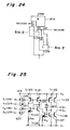
- Fig. 24 shows an example modification of the circuit shown in Fig. 23.
- the relation between the current mirror circuit 51a-1 and the current mirror circuit 51b-1 both shown in Fig. 23 is the one shown in Fig. 21.
- the current mirror circuit which is created by integrating the current mirror circuits 51a-1 and 51b-1 is shown in Fig. 24.
- Fig. 25 shows a specific example of the constant-current ON/OFF typed holding circuit as shown in Fig. 14 using the constant-current ON/OFF typed current switch as shown in Fig. 24.
- Fig. 25 illustrates set input terminals S1 and S2, and a reset input terminals R1 and R2.
- the constant-current ON/OFF typed current switch has a diode d19 whose cathode is connected to the set input terminal S1, a diode d20 whose anode is connected to the reset input terminal S2, a diode d21 whose anode is connected to the set input terminal S2, and a diode d22 whose cathode is connected to the reset input terminal R2.
- the anode of the diode d19 is connected to the cathode of the diode d20.
- the anode of the diode d19 is connected to the collector of the transistor Tr120 and the bases of respective four PNP transistors Tr120, Tr121, Tr122 and Tr123 whose emitters are connected to a power supply V+.
- the collector of the transistor Tr120 is connected to the collector of a NPN transistor Tr124.
- the emitter of the transistor Tr124 is connected to a power supply V- via a resistor Ron.
- the collector of the transistor Tr121 is connected to the collector of a NPN transistor Tr125, and the bases both of the respective transistors Tr125 and Tr124.
- the cathode of the diode d21 is connected to the anode of the diode d22.
- the cathode of the diode d21 is connected to the bases of the transistor Tr124 and Tr125, and the collector of the NPN transistor Tr126.
- the emitter of the transistor Tr125 is connected to the power supply V-.
- the collector of the transistor Tr122 is connected to the collector of a NPN transistor Tr127, the three bases of the transistors Tr127, Tr126 and Tr128, and the anode of the diode d23.
- the cathode of the diode d23 is connected to the power supply V+.
- the emitter of the transistor Tr126 is connected to the power supply V- via the resistor Rth.
- the collector of transistor Tr123 and of transistor Tr128 serve as a current flowing-out output terminal and a current flowing-in output terminal respectively.
- the constant-current source typed current amplifier 51b-2 and the current mirror circuit 51b-1 form the constant-current loop ILPb.
- the output terminal O of the constant-current source typed current amplifier 51b-2 is not connected, on the path making a trip from the common terminal COM of the current mirror circuit 51a-1 through the current mirror circuit 51b-1 to the common terminal COM of the constant-current source typed current amplifier 51b-2, a current which is determined by the constant-current loop ILPb flows.
- the amount of the feedback is determined by the product of gains of the current mirror circuit 51a-1 and the constant-current source typed current amplifier 51a-2. Due to the property of the constant-current source typed amplifier 51a-2, when a current, which flows on the constant-current loop ILPb from which the current mirror circuit 51a-1 inputs, is small, an amount of the feedback is large. Conversely, when the current mentioned above is large, the amount of the feedback is small.
- the feedback loop made from the constant-current source typed amplifier 51a-2 and the current mirror circuit 51a-1 operate effectively to make the loop current gain on the whole circuit less than 1, and thus the current goes to zero.
- the feedback loop made from the constant-current source typed current amplifier 51a-2 and the current mirror circuit 51a-1 can be neglected, and the constant current i on which is determined by the constant-current loop ILPb flows.
- the both currents i on and i th are determined by the band-gap voltage according to a resistance and the ratio of transistor size.
- the currents i on and i th both are determined by the band-gap voltage according to a resistance and the ratio of transistor size.
- the amount of current becomes either more than i th , equal to, or less than i th .
- on and off operations can be conducted with current i on during an on-state and with an absence of current during an off-state respectively.
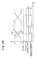
- Fig. 26 is a timing chart for explaining the operation of the circuit shown in Fig. 1. With reference to Fig. 26, the polarity inversion detection circuit of the first embodiment will be described.
- a starting signal or a releasing signal from the exchange is given to a pair of the communication lines L1 and L2.
- the direction of signal inversion on the communication lines L1 and L2 is different.
- polarity inversion occurs in such a way that a first state, where the voltage on the communication line L1 is low and the voltage on the communication line L2 is high changes into a second state where the voltage on the communication line L1 is high and the voltage on the communication line L2 is low.
- the voltage on the communication line L2 from the voltage on the communication line L1 decreases little by little, and soon the voltage between the communication line L1 and the communication line L2 approach zero. At the voltage zero, currents on all circuits are zero, and all the circuits are cleared.
- a power supply voltage according to the voltage between the communication line L1 and the communication line L2, is supplied from the full-wave rectifier to the constant-current ON/OFF typed holding circuit 50, and the constant-current ON/OFF typed holding circuit 50 becomes able to operate properly. Since the ground terminals of the edge detection circuits 30A and 30B are connected to the negative electrode output terminal of the full-wave rectifier 20, it is clamped to the voltage which is higher by the forward voltage of the full-wave rectifier from the lower voltage side between the communication lines L1 and L2.
- the input terminal of the edge detection circuit 30A is connected to the communication line L1. Between the input terminal and the ground terminal of the edge detection circuit 31A, a lower voltage than the voltage between the communication lines L1 and L2 is applied by the forward voltage of the rectifier diode. When the polarity inversion proceeds further, the applied voltage is forced beyond the voltage Von where a current starts flowing and a current Itri starts flowing to the edge detection circuit 30A. When the applied voltage rises further higher and beyond the voltage Voff where no current flows, the current Itri goes to zero and no current flows after then even though the applied voltage still increases.
- the edge detection circuit 30A outputs a first edge detection trigger current Ita in proportion to the current Itri only within the time when a voltage in the polarity inversion transitional period is between Von and Voff. That is, pseudo-differential calculus is performed.
- the input terminal of the edge detection circuit 30B is connected to the communication line L2 which is a low voltage side, and, between the input terminal and the ground terminal, a low voltage only for the forward voltage of the rectifier diode is applied, no current flows. Therefore, no trigger current is outputted from the edge detection circuit 30B.
- the trigger current Ita outputted from the edge detection circuit 30A forces the constant-current ON/OFF typed holding circuit 50 to be set via the OR circuit 40, and therefore a constant current starts flowing on the holding circuit 50.
- a short time pulse of the trigger current Ita is converted to a lasting polarity inversion detection signal and accordingly a polarity inversion information is outputted to the controlling circuit.
- a reset signal is sent from the controlling circuit, thus the constant-current ON/OFF typed holding circuit 50 is reset and returns to a stand-by state.
- a polarity inversion occurs in such a way that a first state, in that the communication line L1 is on a high voltage and the communication line L2 is on a low voltage, is changed into a second state, in that the communication line L1 is on a low voltage and the communication line L2 is on a high voltage, after the communication lines L1 and L2 meet in the same voltage, the communication line L1 becomes a ground potential side and the communication line L2 becomes a high potential side.
- a second edge detection trigger current Itb is outputted from the edge detection circuit 30B and the edge detection circuit 30A stays in an off-state.
- a polarity inversion can be detected by the same operation as described before, except for the operations of the edge detection circuit 30A and the edge detection circuit 30B are exchanged.
- the current Ita and Itb are determined by the band-gap voltage of transistor indifferent with the change dV/dt of the input voltage.
- the voltage V1 sent from a switching system via the communication lines L1 and L2 is almost 48 V (volts). Accordingly, by determining both of the voltage Von, with which a current on each of the edge detection circuits 30A and 30B starts flowing, and the upper-limit voltage Voff, with which a current starts flowing, even though the voltage Vn is noisy during a time T as shown in Fig. 26, the input voltages of the edge detection circuits 30A and 30B are not below the voltage Voff. Therefore, no malfunction is made to output an error trigger. 0 ⁇ Von ⁇ Voff ⁇ 48 V (48 V - Voff) > (noise level Vn during stand-by)
- the polarity inversion detection circuit of the first embodiment is created by the combination of the edge detection circuits 30A and 30B as described in the section [I] (2).
- the edge detection circuits 30A and 30B have the following advantages (1 - 1) to (1 - 4).
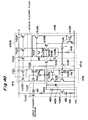
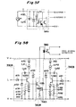
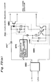
- Fig. 27 illustrates a configuration of the polarity inversion detection circuit of the second embodiment according to the present invention.
- Common reference numerals are attached to elements which are the same as the ones shown in Fig. 1.
- the polarity inversion detection circuit is for a telemetering apparatus to detect polarity inversion information, as either a starting signal or a releasing signal, from a pair of the communication lines L1 and L2.
- the polarity inversion detection circuit has a full-wave rectifier 20 which outputs a constant polarity voltage by full-wave rectifying the current flowing on the communication lines L1 and L2, a first edge detection circuit 30A which detects a polarity inversion edge on either the starting signal or the releasing signal and outputs a first edge detection trigger current Ita, and a second edge detection circuit 30B which detects a polarity inversion edge on either the starting signal or the releasing signal and outputs a second edge detection trigger current Itb.
- the full-wave rectifier 20 and the edge detection circuits 30A and 30B have the same configurations as the ones described in the first embodiment, and they are connected to the communication lines L1 and L2 in the same manner as described in the first embodiment.
- a constant-current ON/OFF & change-over typed holding circuit 60 is connected between the positive electrode terminal (+) and the negative electrode terminal (-) of the full-wave rectifier 20.
- the trigger currents Ita and I tb from the edge detection circuits 30A and 30B respectively is inputted to the constant-current ON/OFF & change-over typed holding circuit 60.
- a reset signal from an external circuit is inputted.
- the constant-current ON/OFF & change-over typed holding circuit 60 has three output terminals.
- Fig. 28 illustrates a configuration of the constant-current ON/OFF & change-over typed holding circuit 60.
- the constant-current ON/OFF & change-over typed holding circuit 60 has a current mirror circuit M20, an interface circuit 61, a constant current ON/OFF typed switch 62, a current change-over typed switch 63, and photo couplers 64 and 65 both of which are connected to the current change-over typed switch 63.
- the current mirror circuit M20 is made from the current mirror circuit which is selected from the circuits shown in Fig. 4 described in the first embodiment.
- the common terminal COM of the current mirror circuit M20 is connected to a power supply V+.
- the constant-current ON/OFF typed switch 62 has the same configuration as the constant-current ON/OFF typed switch 62 shown in Fig. 14 through Fig. 24 in the first embodiment.
- the input terminal I of the current mirror circuit M20 is connected to a terminal of the constant-current flowing-in side of the constant-current ON/OFF typed switch 62.
- a terminal of the constant-current flowing-out side of the constant-current ON/OFF typed switch 62 is connected to the positive power supply terminal of the current change-over typed switch 63 while a negative power supply terminal of the current change-over typed switch 63 is connected to a power supply V-.
- the current change-over typed switch 63 has current output terminals Q and Q/, and select either Q or Q/ to output a current according to the selection.
- the photo coupler 64 as a first output circuit is connected to the current output terminal Q while the photo coupler 65 as a second output circuit is connected to the other current output terminal Q/.
- the destination of outputting from the photo couplers 64 and 65 is the controlling circuit which has different ground levels.
- the trigger current Ita outputted from the edge detection circuit 30A indicates a polarity inversion on the starting side and the releasing side.
- the trigger current Ita is inputted to the input terminal IN1 of the interface circuit 61.
- the trigger current Itb outputted from the edge detection circuit 30B indicates a polarity inversion on the starting side and the releasing side.
- the trigger current Itb is inputted to the input terminal IN2 of the interface circuit 61.
- the output terminal O1 corresponding to the input terminal IN1 of the interface circuit 61 is connected to the set terminal S of the current change-over typed switch 63.
- the output terminal O2 corresponding to the input terminal IN2 of the interface circuit 61 is connected to the reset terminal R of the current change-over typed switch 63.
- the output terminal O3, from which the result of OR operation of signals outputted from the input terminals IN1 and IN2 of the interface circuit, is connected to the set terminal S of the constant-current ON/OFF typed switch 62.
- a reset signal from the controlling circuit is inputted to the reset terminal R of the constant-current ON/OFF typed switch 62.
- the output terminal of the current mirror circuit M20 is the output terminal (Q1 + Q2) of the constant-current ON/OFF & change-over typed holding circuit 60.
- Fig. 29 (a) and (b) illustrate specific example circuits of the current change-over typed switch 63 shown in Fig. 28.
- the circuit shown in Fig. 29 (a) has four NPN transistors Tr131 through Tr134. Between the collector of a transistor Tr131 and a positive power supply terminal, a load resistor Rc1 is connected. Between the collector of a transistor Tr132 and a positive power supply terminal, a load resistor Rc1 is connected. Between the collector of the transistor Tr131 and the base of the transistor Tr132, a resistor Rbl is connected, while, between the collector of the transistor Tr132 and the base of the transistor Tr131, a resistor Rb2 is connected.
- the bases of a transistors Tr133 and Tr134 are a set input terminal S and a reset input terminal of the current change-over typed switch 63 respectively.
- the combination of transistors Tr133 and Tr134 form a trigger input buffer transistors.
- the collector of the transistor Tr133 as the trigger input buffer transistor is connected to the collector of the transistor Tr131.
- the collector of the transistor Tr134 as the trigger input buffer transistor is connected to the collector of the transistor Tr132.
- the emitters of the transistors 131 through 134 all are connected to a negative power supply terminal. Both ends of the load resistor Rc1 are a current output terminal Q while both ends of the load resistor Rc2 is a current output terminal Q/.
- the photo couplers 64 and 65 (not shown) are connected to the current output terminals Q and Q/.
- the circuit shown in Fig. 29 (b) also has four NPN transistors Tr141 through Tr144. Between the collector of the transistor Tr141 and a positive power supply terminal, a load resistor Rc3 is connected. Between the collector of the transistor Tr142 and a positive power supply terminal, a resistor Rc4 is connected. Between the collector of the transistor Tr141 and the base of the transistor Tr142, a resistor Rb3 is connected while, between the collector of the transistor Tr142 and the base of the transistor Tr141, a resistor Rb4 is connected.
- the bases of the transistors Tr143 and Tr144 are connected to a set input terminal S and a reset input terminal R respectively.
- the combination of the transistors 143 and 144 forms a trigger input buffer transistors.
- the collector of the transistor 14 as a trigger input buffer transistor is connected to the base of the transistor Tr142.
- the collector of transistor Tr144 as a trigger input buffer transistor is connected to the base of the transistor Tr141.
- the emitters of the transistors 141 through 144 all are connected to the negative power supply terminal. Both ends of a load resistor Rc3 are current output terminals Q while both ends of a load resistor Rc4 are current output terminals Q/.
- the circuits shown in Fig. 29 (a) and (b) are a well-known positive feedback loop circuit.
- a transistor Tr131 or a transistor Tr132 starts changing into an on-state, the other starts changing into an off-state.
- Any one of the transistors Tr131 and Tr132 can be turned into an on-state by a trigger current which is inputted from a set input terminal S or a reset input terminal R, and in a stable state one transistor is in an on-state while the other is in an off-state.
- the transistors Tr141 and Tr142 operate the same as the operations of the transistors Tr131 and 132.
- Fig. 30 (a) through (d) and Fig. 31 (a) through (b) illustrate specific example circuits of the interface circuit shown in Fig. 28.
- the interface circuit 61 has a configuration in that between a first circuit which is connected at the input terminals IN1 and IN2 and the constant-current ON/OFF typed switch 62 which is connected to an output terminal O3, and between the first circuit and the current change-over typed switch 63 which is connected to output terminals O2 and O3 , the interface circuit 61 determines same current directions (a terminal IN1 ⁇ a terminal O1) and (a terminal IN2 ⁇ a terminal O2) so that the constant-current ON/OFF typed switch 62 and the current change-over typed switch 63 can be well-operated by output currents from the first circuit. Moreover, the interface circuit 61 realizes an OR operation between the input terminals IN1 and IN2 and determines same current direction ((the terminals IN1 and IN2) ⁇ a terminal O3).
- An inversion of current directions is conducted by an internal current mirror circuit, and an OR operation is performed by a wired-OR configuration.
- a trigger pulse current is inputted to the input terminal IN1, it is forwarded to both of the terminals O1 and O3.
- a trigger pulse current is inputted to the input terminal IN2, it is forwarded to the terminals O2 and O3.
- Fig. 30 (a) shows an interface circuit which inputs on- and off-currents and which has current mirror circuits M21 and M22 both in which common terminals COM are connected to a power supply V-.
- the input terminal IN1 is connected to the output terminal O1 in the interface circuit and also connected to the input terminal I in the current mirror circuit M21.
- the output terminal O in the current mirror circuit M21 is connected to the output terminal O3 in the interface circuit via a wired OR 61a.
- the input terminal IN2 is connected to the output terminal O2 in the interface circuit and also connected to the input terminal I in the current mirror circuit M22.
- the output terminal O in the current mirror circuit M22 is connected to the output terminal O3 via the wired OR 61a.
- Fig. 30 (b) also shows an interface circuit which inputs an on-and off-current, and has current mirror circuits M23 and M24 both whose common terminals are connected to a power supply V-, and a current mirror circuit M25 whose common terminal is connected to a power supply V+.
- the input terminal IN1 is connected to the output terminal O1 in the interface circuit, and also connected to the input terminal in the current mirror circuit M23.
- the output terminal of the current mirror circuit M23 is connected to the input terminal I in the current mirror circuit M25.
- the input terminal IN2 is connected to the output terminal O2 in the interface circuit, and also connected to the input terminal I in the current mirror circuit M24.
- the output terminal in the current mirror circuit M25 is connected,to the output terminal O3 in the interface circuit.
- Fig. 30 (c) shows an interface circuit which inputs an on- and off-flowing-out currents, and which has current mirror circuits M26 and M27, both of which have two outputs, whose common terminals are connected to a power supply V+.
- the input terminal IN1 is connected to the input terminal of the current mirror circuit M26 while the input terminal IN2 is connected to the input terminal I of the current mirror circuit M27.
- One output terminal of the current mirror circuit M26 is connected to the output terminal O1 of the interface circuit, the other output terminal is connected to the output terminal O3 of the interface circuit via a wired-OR 61c.
- One output terminal of the current mirror circuit M27 is connected to the output terminal O2 of the interface circuit while the other output terminal is connected to the output terminal O3 via the wired-OR 61c.
- Fig. 30 (d) also shows a interface circuit which inputs on- and off- flowing-out currents, and has current mirror circuits M28 and M29, both of which have two outputs, whose common terminals COM are connected to a power supply V+, and a current mirror circuit M30 whose common terminal is connected to a power supply V-.
- the input terminal IN1 is connected to the input terminal I of the current mirror circuit 28 while the input terminal IN2 is connected to the input terminal I of the current mirror circuit M29.
- One output terminal of the current mirror circuit M28 is connected to the output terminal O1 of the interface circuit while the other output terminal is connected to the input terminal I of the current mirror circuit M30 via a wired-OR 61d.
- One output terminal of the current mirror circuit M29 is connected to the output terminal O2 of the interface circuit while the other output terminal is connected to the input terminal I of the current mirror circuit M30 via a wired-OR 61d.
- the output terminal O of the current mirror circuit M30 is connected to the output terminal O3 of the interface circuit.
- Fig. 31 (a) shows an interface circuit whose input terminal has both current flowing-in and -out modes.
- the interface has diodes d61 and d62 whose cathodes both are connected to a power supply V-.
- a current flowing-in side of the input terminal IN1 is connected to the output terminal O1 of the interface circuit, and also connected to the anode of the diode d61.
- a current flowing-in side of the input terminal IN2 is connected to the output terminal O2 of the interface circuit, and also connected to the anode of the diode d62.
- Current output sides of the input terminals IN1 and IN2 are wired-OR connected (wired-OR 61e), and also connected to the output terminal O3 of the interface circuit.
- Fig. 31 (b) also shows an interface circuit whose input terminal has current flowing-in and -out modes, and has diodes d63 and d64, whose both cathodes are connected to a power supply V-, and a current mirror circuit M31 whose common terminal is connected to a power supply V+.
- a current flowing-in side of the input terminal IN1 is connected to the output terminal O1 of the interface circuit, and also connected to the anode of the diode d63.
- a current flowing-in side of the input terminal IN2 is connected to the output terminal O2 of the interface circuit, and also connected to an anode of the diode d64.
- Fig. 30 (a) and (c) and Fig. 31 (a) illustrate interface circuits each of which is used for a constant-current ON/OFF typed switch 62 (e.g. as shown in Fig. 16, Fig. 18, Fig. 20, Fig. 21, and Fig. 22) which is located at the last step and which turns into an on-state by a flowing-out current trigger.
- Fig. 30 (b) and (d) and Fig. 31 (b) illustrate interface circuits (e.g. as shown in Fig. 17 and Fig. 19) each of which turns into an on-state by a flowing-in current.
- the trigger current Ita is supplied to both set input terminals S of the respective current change-over typed switch 63 and constant-current ON/OFF typed switch 62 form the interface circuit 61. Consequently, the constant-current ON/OFF typed switch 62 turns into an on-state, currents flows on the current change-over typed switch 63 and current mirror circuit M20, and thus a constant current flows from the output terminal O of the current mirror circuit.
- the trigger current Itb When a trigger current Itb is inputted via the input terminal IN2 in a stand-by state, the trigger current Itb is supplied to the reset input terminal R of the current change-over typed switch 63 and the set input terminal S of the constant-current ON/OFF typed current switch 62 from the interface circuit 61. Consequently, the constant-current ON/OFF typed switch 62 turns into an on-state, currents flow on the current change-over typed switch 62 and the current mirror circuit M20, and a constant current is outputted from the output terminal O of the current mirror circuit M20.
- the photo coupler 64 When the constant-current ON/OFF typed switch 62 is in an on state, the photo coupler 64 is in an on-state in accordance with a current outputting from the output terminal Q of the current change-over typed switch 63, the photo coupler 65 is in an off-state, and the current mirror circuit M20 continues to output a constant current, when a trigger current Itb is inputted from the input terminal IN2, the trigger current is inputted into both of the reset input terminal R of the current change-over typed switch 63 and the set input terminal S of the constant-current ON/OFF typed current switch 62. Thereby, a current is sent from the output terminal Q/ and flown into the photo coupler 65, and a current sent from the output terminal Q is stopped. That is, no current flows on the photo coupler 64. The current mirror circuit M20 continues to output a constant current.
- the photo coupler 65 When the constant-current ON/OFF typed switch 62 is in a on-state, the photo coupler 65 is in an on-state in accordance with a current outputting from the output terminal of the current change-over typed switch 63, the photo coupler 64 is in an off-state in accordance with no current supplied from the output terminal Q, and the current mirror circuit M20 continues outputting a constant current, when a trigger current Ita is inputted from the input terminal IN1, a trigger current is inputted to the set input terminals S of the current change-over typed switch 63 and the constant-current ON/OFF typed switch 62, and the output terminal Q outputs a current which flows on the photo coupler 64.
- the current mirror circuit M20 continues outputting a constant current.
- the constant-current ON/OFF typed switch 62 receives a reset signal, all outputs return to an off-state.
- the trigger current Ita is inputted from the input terminal IN1
- the photo coupler 64 turns into an on-state and the photo coupler 65 turns into an off-state.
- the trigger current Itb is inputted from the input terminal IN2
- the photo coupler 65 turns into an on-state and the photo coupler 64 turns into an off-state.
- the current mirror M20 turns into an on-state to output a current when either a trigger current from the input terminal IN1 or a trigger current from the input terminal IN2 is inputted. That is, the result of a polarity inversion detection is held.
- Fig. 32 is a timing chart showing the operation of the polarity inversion detection circuit shown in Fig. 27. With reference to Fig. 32, the operation of the polarity inversion detection circuit of the second embodiment will be detailed.
- the direction of the polarity inversion on the communication lines L1 and L2 is opposite.
- operations on the circuit when a polarity inversion occurs from a first state, in that the communication line L1 is in a low electrical potential and the communication line L2 is in a high electrical potential, to a second state, in that the communication line L1 is in a high electrical potential and the communication line L2 is in a low electrical potential, will be described below.
- the constant-current ON/OFF & change-over typed holding circuit 60 is supplied with a power supply voltage according to the potential difference between the communication lines L1 and L2 from the full-wave rectifier 20, and the constant-current ON/OFF & change-over typed holding circuit 60 reaches an normally operable state.
- Ground terminals G of the edge detection circuits 30A and 30B are connected to a negative electrode terminal (-), and thus electric potentials on the ground terminals G are clamped on a higher electric potential, by the forward voltage of a rectifier diode, than a lower electric potential side (L2 is a lower side at this time) between the communication lines L1 and L2.
- the input terminal of the edge detection circuit 30A is connected to the communication line L1. Between the input terminal of the edge detection circuit 30A and the ground terminal G, a voltage is applied which is lower than the potential difference between the communication lines L1 and L2 by the forward voltage of a rectifier diode. When the polarity inversion proceeds furthermore, the voltage goes beyond the voltage Von where a current starts flowing, and a current Itri flows on the edge detection circuit 30A. When the voltage increases further and goes beyond the voltage Voff where no current flows, the current Itri becomes zero. After this, even though the voltage increases further, no current flows.
- the edge detection circuit 30A outputs the trigger current Ita in proportion to the current Itri only during a short time between Von and Voff wherein the voltage becomes, in the polarity inversion transient time. That is, a pseudo-differential calculus is attained. Further, the input terminal of the edge detection circuit 30B is connected to the communication line L2 which is in a lower electrical potential. Since a lower voltage by the forward voltage of a rectifier diode is applied between the input terminal and the ground terminal G, no current flows. Therefore, no trigger current is outputted from the edge detection circuit 30B.
- Trigger currents outputted from the edge detection circuit 30A and 30B , as edge detection trigger signals, are inputted to the interface circuit 61 of the constant-current ON/OFF & change-over typed holding circuit 60.
- the interface circuit 61 generates a trigger signal which starts a change-over operation on the current change-over typed switch 63 by processing the signal level of the edge detection trigger current from the edge detection circuits 30A and 30B, and a trigger current which forces the constant-current ON/OFF typed switch 62 to change into an on-state by processing and ORing the signal level.
- the constant-current ON/OFF & change-over typed holding circuit 60 receives a trigger current Ita from the edge detection circuit 30A, it forces the constant-current ON/OFF typed switch 62 to be turned into an on-state, forces a constant current, which is a common current of the current change-over typed switch 63, and outputs a current from the output terminal Q of the current change-over typed switch 62 (and thus the photo coupler 64 is turned into an on-state).
- the constant-current ON/OFF & change-over typed holding circuit 60 forces the constant change-over typed switch 62 to be turned into an on-state, which causes a common constant current to be flown on the current change-over typed switch 63, and outputs a current from the output terminal Q/ of the current change-over typed switch 63 (and thus the photo coupler 65 is turned in an on-state).
- the edge detection circuit 30A or the edge detection circuit 30B Dependent upon the direction of a polarity inversion, only one of either the edge detection circuit 30A or the edge detection circuit 30B detects a polarity inversion edge and that operating circuit outputs either trigger pulse current Ita or Itb respectively. Accordingly, a current is outputted from either an output terminal Q or an output terminal Q/ of the constant-current ON/OFF & change-over typed holding circuit 60.
- the edge detection circuits 30A and 30B output the trigger currents Ita and Itb alternatively in accordance with the polarity inversion. Accordingly, the constant-current ON/OFF & change-over typed holding circuit 60 outputs currents from the output terminals Q and Q/ alternatively. Next, a current is outputted from either the output terminal Q or the output terminal Q/ in accordance with the last polarity state.
- the constant-current ON/OFF & change-over typed holding circuit 60 does not need to hold the polarity inversion information, like when a communication is ended, it is reset by a reset signal from the controlling circuit and returns to a stand-by state.
- the polarity inversion detection circuit of the second embodiment has a configuration in that a polarity inversion on the communication lines L1 and L2 is detected using the edge detection circuits 30A and 30B which is the same as the ones described in the first embodiment. It has the same advantages as described in the sections (1 - 1) through (1- 7) in the first embodiment. Moreover, the polarity inversion circuit of the second embodiment has a constant-current ON/OFF & change-over typed holding circuit 60.
- the constant-current ON/OFF & change-over typed holding circuit 60 amount of currents both flowing on the photo couplers 64 and 65 are determined in accordance with the constant current of the constant-current ON/OFF typed switch 62 as same as described in Fig. 1. Thus, one resistor determines both current amounts without dispersion.
- two holding circuits are necessary in accordance with the respective photo couplers. Therefore, there is a possibility that a malfunction in which both are turned into on-states occurs.
- three output states i.e. only photo coupler 64 is on, only photo coupler is on, and both are off
- the polarity inversion detection circuit shown in Fig. 27 has the following (2 -1) to (2 - 7) advantages.
- Fig. 33 illustrates the whole configuration of the slow polarity inversion detection circuit of the third embodiment in accordance with the present invention.
- Telemetering communication can be available when a telephone line is not busy. There is the following difference between normal communication and telemetering communication:
- the conventional polarity inversion circuit and the polarity inversion detection circuits of the first and second embodiments can detect both of the above polarity inversions, but, cannot distinguish between the slow polarity inversion and the normal polarity inversion, in which the time of the slow polarity inversion is longer than that of the normal polarity inversion.
- the two kinds of communications described above can only be distinguished by detecting whether or not a bell signal is sent after the polarity inversion.
- a normal communication has 100% priority over a telemetering communication, which is possible when the line is not being used for normal communication. Therefore, for the communication to succeed, it is important that the telemetering communication be completed in the shortest possible time. The several seconds for determining whether a bell signal is received or not make the communication line unavailable.
- the slow polarity inversion detection circuit of the third embodiment detects a slow polarity inversion, that it to say, distinguish the slow polarity inversion from the normal inversion. This immediately permits starting of telemetering communication processing, independent from whether or not a bell signal follows.
- the slow polarity inversion detection circuit shown in Fig. 33 has two rectifiers 100 and 110.
- the first rectifier 100 which rectifies in full-wave form the voltage between the communication lines L1 and L2 and provides the next circuit with power-supplies V+ and V-.
- the second rectifier 110 rectifies the voltage between the communication lines L1 and L2 and provides one electrode of a power supply capacitor Cp30 with a power supply via a current control resistor R70.
- the other electrode of the capacitor Cp30 is connected to the negative electrode terminal (-) of the rectifier 100.
- two polarity inversion trailing edge detection circuits 120 and 130, and a constant current ON/OFF monostable multivibrator 140 are connected.
- the polarity inversion trailing edge detection circuit 120, the full-wave rectifier 100, the rectifier 110, the resistor R70 and the capacitor Cp30 form a first polarity inversion trailing edge detection circuit K1 (described later), which detects a polarity inversion trailing edge whose electric potential descent on the communication line L1 is (H ⁇ 0).
- the polarity inversion trailing edge detection circuit 130, the full-wave rectifier 100, the rectifier 110, the resistor R70 and the capacitor Cp30 form a second polarity inversion trailing edge detection circuit K2 (described later), which detects a polarity inversion trailing edge whose electric potential descent on the communication line L2 is (H ⁇ 0).
- an OR circuit 150 is placed on the output sides of the polarity inversion trailing edge detection circuits 120 and 130.
- output trigger currents from the polarity inversion trailing edge detection circuits 120 and 130 are processed, and the result is inputted to the constant-current ON/OFF monostable multivibrator 140.
- the constant-current ON/OFF monostable multivibrator 140 inputs a trigger current from the OR circuit 150 and outputs a constant-current pulse (i.e. a pulse for masking a polarity inversion detection on a normal communication).
- a polarity inversion leading edge detection circuit 160 is connected to detect a polarity inversion leading edge when the electric potential rises (0 ⁇ H) on the communication line L1.
- a second polarity inversion leading edge detection circuit 170 is connected to detect a polarity inversion leading edge when an electric potential rises (0 ⁇ H) on the communication line L2.
- An OR circuit 190 is placed as a second detection signal generation circuit on the output sides of the polarity inversion leading edge detection circuits 160 and 170 to process output trigger currents from the polarity inversion leading edge detection circuits 160 and 170.
- an OR circuit 180 is placed as a reset pulse generation circuit on the output side of the constant-current ON/OFF monostable multivibrator 140, which responds to an external reset signal from the controlling circuit and an output signal from the constant-current monostable multivibrator 140.
- the positive and negative electrode terminals of the full-wave rectifier 100 are connected to a holding circuit 200, which is supplied with power supplies V+ and V-.
- the set input terminal S of the holding circuit 200 is connected to the output terminal of the OR circuit 190, while the reset input terminal R of the holding circuit 200 is connected to the output terminal of the OR circuit 180.
- the holding circuit 200 is configured such that polarity inversion information is held in accordance with pulse currents from the respective OR circuits 180 and 190 and outputted to the controlling circuit.
- the polarity inversion leading edge detection circuits 160 and 170 have the same internal configuration as the edge detection circuits 30A and 30B.
- the polarity inversion leading edge detection circuits 160 and 170 each performs a pseudo-differential operation using a circuit which outputs a constant current Itri when the applied voltage between the input terminal and the ground terminal is within the range from Von to Voff (on condition that Von ⁇ Voff). More specifically, the trigger currents Ita and Itb are outputted in accordance with a leading edge in which, on a communication line with a lower electric potential, the lower electric potential rises from zero to a higher electric potential.
- the polarity inversion trailing edge detection circuits 120 and 130 (will be detailed later), have a configuration such that the edge detection circuits 30A and 30B, each with a current mirror diode and a backward-current-proof diode perform a pseudo-differential operation to detect a polarity inversion trailing edge.
- the polarity inversion trailing edge detection circuits 120 and 130 each outputs a constant current Itri when the electric potential difference between the positive power supply terminal and the input terminal is within the range from VL to VH (on condition that VL ⁇ VH). More specifically, a trigger current is outputted in accordance with a trailing edge in which, on a communication line with a higher electric potential, which is connected to the input terminal of the polarity inversion trailing edge detection circuit, the higher electric potential falls to zero.
- the constant-current ON/OFF monostable multivibrator 140 is inputted the trigger current and outputs a guaranteed current pulse. Since the constant-current ON/OFF monostable multivibrator 140 (will be described in detail later)only outputs a pulse when current flows through it, thereby consuming no electric power during stand-by.
- the holding circuit 200 has a switch circuit which enables or disables current flow (the current flows when a set signal is inputted; no current flows when a reset signal is inputted, on condition that a priority is given on the reset), a current mirror circuit, which outputs current in accordance with the output of the switch circuit, and a photo coupler which transfers polarity inversion information to the controlling circuit with a different ground level.
- the holding circuit 200 for example, can be configured in the same way as the circuit shown in Fig. 14 of the first embodiment.
- OR circuits 150, 180 and 190 all perform an OR operation on current signals, which are realized with a wired-OR configuration.
- the polarity inversion trailing edge detection circuit is configured from a pulse trailing edge detection circuit for detecting a trailing edge of an input pulse.
- the pulse trailing edge detection circuit will be described in subsection [VII] (1) (i).
- the configuration of the polarity inversion trailing edge detection circuit and the operation of the polarity inversion trailing edge detection circuits K1 and K2 will be described in subsections [VII] (1)(ii) and [VII] (1) (iii), respectively.
- Fig. 34 illustrates a configuration of the pulse trailing edge detection circuit.
- the pulse trailing edge detection circuit has a trailing edge detection circuit 210 and a peak holding circuit 220.
- the trailing edge detection circuit 210 has a circuit 211, two linear current mirror circuit M40 and M41 and a backward-current-proof diode 212.
- constant current flows within a predetermined constant-voltage range. This is also used for the polarity inversion leading edge detection circuit.
- the first linear current mirror circuit M40 has a current flowing-out input terminal Ip, two current flowing-out output terminals Op1 and Op2, and a common terminal COMp to which current flows in, the total amount of which is equal to the total current flowing through the two current flowing-out output terminals Op1 and Op2.
- the second linear current mirror circuit M41 has a current flowing-in input terminal I n1 , two current flowing-in output terminals O n1 and O n2 , and a common terminal COMn, from which current flows out, the amount of which is equal to the total amount flowing-out of the two current flowing-out output terminals O n1 and O n2 .
- the peak holding circuit 220 has a rectifier diode and a capacitor 222 for the peak holding.
- the constant current circuit shown in Fig. 13 (a) and Fig. 13 (d) in the first embodiment can be used.
- Fig. 35 shows wave-shapes of an input voltage and an output current in terms of the circuit 211 shown in Fig. 34 in which constant current flows within a predetermined constant voltage range.
- the common terminal COMp of the current mirror circuit M40 is used as a positive power supply terminal of the trailing edge detection circuit 210 while the common terminal COMn of the current mirror circuit M41 is used as a negative power supply terminal of the trailing edge detection circuit 210.
- the input terminal Ip of the current mirror circuit M40 is connected to the current flowing-in terminal of the circuit 211.
- the current flowing-out terminal of the circuit 211 is connected to the anode of the backward-current-proof diode 212.
- the input terminal In of the current mirror circuit M41 is connected to the output terminal Op1.
- the cathode of the diode 212 is connected to the output terminal On1of the current mirror circuit M41, which is an input terminal IN of the trailing edge detection circuit 210.
- the output terminal Op2 of the current mirror circuit M40 and the output terminal On2 of the current mirror circuit M41 are output terminals OUT of the trailing edge detection circuit 210, but either the output terminal Op2 or the output terminal On2 can be omitted if unnecessary.
- the capacitor 222 is connected between the output terminal and a ground terminal.
- the input terminal of the trailing edge detection circuit 210 and the input terminal of the peak holding circuit 220 are both connected to the signal line L, and the output terminal of the peak holding circuit 220 is connected to the positive power supply terminal COMp of the trailing edge detection circuit 210.
- the negative power supply terminal COMn of the trailing edge detection circuit 210 and the ground line of the peak holding circuit 220 are both connected to a signal ground line Lg.
- the current mirror circuit M40 in the trailing edge detection circuit 210 can be configured as a part of the circuit 211, and a specific example of this is shown in Fig. 36.
- Fig. 36 (a) and (b) are specific example circuits of the trailing edge detection circuit 210 shown in Fig. 34.
- the edge detection circuit shown in Fig. 36 (a) has four PNP transistors Tr151 through Tr154 whose emitters are connected to a positive power supply terminal.
- the collector of the transistor Tr151 is connected to the cathode of a Zener diode d71 while the anode of the Zener diode d71 is connected to the cathode of a Zener diode d72.
- the anode of the diode d72 is connected to the collector and the base of a transistor Tr155, while the emitter of the transistor Tr155 is connected to one end of a resistor Rth.
- the collector of the transistor Tr152 is connected to the bases of the transistors Tr151 through Tr154, and also connected to the emitters of two PNP transistors Tr156 and Tr157.
- the collector of the transistor Tr156 is connected to the bases of the transistors Tr156 and Tr157 and also connected to the collector of an NPN transistor Tr158.
- the emitter of the transistor Tr158 is connected to one end of a resistor Ron.
- the collector of the transistor Tr157 is connected to the cathode of a Zener diode d73 while the anode of the Zener diode d73 is connected to the bases of the transistor Tr158 and an NPN transistor Tr159 and the collectors of the NPN transistor Tr159 and an NPN transistor Tr160.
- the base of the transistor Tr160 is connected to the base of the transistor 155.
- the other end of the resistor Rth, the other end of the resistor Ron, and the emitters of the transistors Tr159 and Tr160 are connected to the anode of a diode d74.
- the diode d74 is equivalent to the diode shown in Fig. 34.
- the cathode of the diode d74 is connected to the collector of the NPN transistor Tr161.
- the collector of the transistor Tr153 is connected to the base of the transistor Tr161, and to the base and the collector of the NPN transistor Tr163, and to the base of the transistor Tr163.
- the emitters of the transistors Tr161 through Tr163 are connected to a ground.
- the collector of the transistor Tr154 is the output terminal Op2 of the current mirror circuit M40 while the collector of the transistor Tr163 is the output terminal On2 of the current mirror circuit M41.
- the emitters of four PNP transistors Tr171 through Tr174 are connected to the positive power supply terminal.
- the collector of the transistor Tr171 is connected to the bases of transistors Tr171 through Tr174, and connected to the cathode of a Zener diode d75.
- the anode of the diode d75 is connected to the emitter of a PNP transistor Tr175 while the collector of the transistor Tr175 is connected to the cathode of a Zener diode d76.
- the anode of the diode d76 is connected to the collector and the base of the NPN transistor Tr176 while the emitter of the transistor Tr176 is connected to one end of the resistor Rth.
- the collector of the transistor Tr172 is connected to the emitter of a PNP transistor Tr177.
- the collector of the transistor Tr177 is connected to the bases of the transistor 177 and the transistor Tr175, and also connected to the emitters of the PNP transistors Tr178 and Tr179.
- the collector of the transistor Tr178 is connected to the emitter of the PNP transistor Tr180 while the collector of the transistor Tr180 is connected to the bases of the transistors Tr180 and Tr182 and to the collector of the transistor Tr181.
- the emitter of the transistor Tr181 is connected to one end of the resistor Ron.
- the collector of the transistor Tr179 is connected to the bases of the transistors Tr178 and Tr179, and to the emitter of a PNP transistor Tr182.
- the base of the transistor Tr182 is connected to the base of the transistor Tr180.
- the collector of the transistor Tr182 is connected to the collector and the base of the NPN transistor Tr183, the base of the transistor Tr181, and the collector of the NPN transistor Tr184.
- the base of the transistor Tr184 is connected to the base of the transistor Tr176.
- the collector of the transistor Tr173 is connected to the emitter of a NPN transistor Tr185.
- the collector of the transistor Tr174 is connected to the emitter of an PNP transistor Tr186.
- the bases of the transistors Tr185 and Tr186 are connected to the collector of the transistor Tr177.
- the other end of the resistor Rth, the other end of the resistor Ron, the emitter of the transistor Tr183, and the emitter of the transistor Tr184 are connected to the anode of a diode d77.
- the diode d77 is equivalent to the diode shown in Fig. 34.
- the cathode of the diode d77 is connected to the collector of an NPN transistor Tr187 while the emitter of the transistor Tr187 is connected to the ground.
- the collector of the transistor Tr185 is connected to the base of the transistor Tr187, to the base and the collector of the NPN transistor Tr188, and to the base of the NPN transistor Tr189.
- the collector of the transistor Tr186 is the output terminal Op2 of the current mirror circuit M40 while the collector of the transistor Tr189 is the output terminal On2 of the current mirror circuit M41.
- the circuit 211 through which a constant current flows within a predetermined constant voltage, is designed in such a way that current flows within the range from VL to VH (where O ⁇ VL ⁇ VH ⁇ Vp) wherein VL denotes the voltage by which current starts flowing, VH denotes the voltage by which current stops flowing, and Vp denotes the peak value of an input pulse.
- the loop current amplification factor on the path making a trip from the current flowing-out input terminal Ip to the current flowing-in output terminal On1(Ip ⁇ Op1 ⁇ In ⁇ On1) is set to almost 1.
- the current amplification factor is less than 1, an input current starts flowing out when a trailing edge detection trigger current is outputted. Otherwise, in the case that the current amplification factor is 1 or more, when the trailing edge detection trigger current is outputted, an input current starts flowing in. Influence to the input current is minimum when the current amplification factor is almost 1.
- the peak holding circuit 220 charges and holds the peak value of the pulse voltage, and supplies it to the positive power supply terminal COMp of the trailing edge detection circuit 210.
- the level of the input terminal IN of the trailing edge detection circuit 210 is the same as the peak voltage of an inputted pulse.
- the backward-current-proof diode 212 prevents a backward voltage from being applied on the circuit 211 when the rising velocity of the inputted pulse is large.
- a constant current which is determined by the circuit 211, flows within a short time when the voltage ⁇ V on the a trailing edge of a pulse is between VL and VH.
- a pseudo-differential operation is made to detect the trailing edge of the pulse. This operation is made using the electric energy accumulated in the capacitor 222 in the peak holding circuit 220.
- the peak holding circuit 220 holds an electric charge for detecting a trailing edge and outputting a its detection signal, and prepares for the next pulse trailing edge detection. That is, a pulse trailing edge is detected and thus a trigger current as shown in Fig. 35 is outputted.
- the pulse trailing edge detection circuit as described above has the following advantages.
- Fig. 37 illustrates a configuration of the polarity inversion trailing edge detection circuit K1.
- the first and second polarity inversion trailing edge detection circuits connected to the balanced communication lines L1 and L2 are dependent upon the pulse trailing edge detection circuit shown in Fig. 34.
- a specific example of the first polarity inversion trailing edge detection circuit K1 is shown in Fig. 37.
- the polarity inversion trailing edge detection circuit K1 is configured such that the peak holding circuit 220 in the pulse trailing edge detection circuit shown in Fig. 34 is replaced with the peak holding circuit 220a which comprises the full-wave rectifier 110, the current control resistor R70 and the power supply capacitor Cp30 as shown in Fig. 33. Moreover, the full-wave rectifier circuit 100 for supplying an electric power to a circuit connected to the peak holding circuit 220a is added. Thus, the circuit configuration of the polarity inversion trailing edge detection circuit 120 is designed similar to the polarity inversion trailing edge detection circuit 210.
- the constant-current circuit 211 through which a constant current flows within a predetermined constant voltage range is configured such that a current flows within VL through VH (on condition that 0 ⁇ Op1 ⁇ In ⁇ Onl) where VL denotes the voltage at which current starts flowing, VH denotes the voltage at which current stops flowing, and Vp denotes the voltage between the communication lines during stand-by.
- the constant-current circuit 211 on which a constant current flows within a predetermined constant voltage range, is designed in such a way that current flows within the voltage range from VL through VH (on the condition that 0 ⁇ VL ⁇ VH ⁇ Vp).
- the communication line L1 is connected to the input terminal I of the polarity inversion trailing edge detection circuit 210. Accordingly, a polarity inversion trailing edge, in which the electric potential on the communication line L1 goes to zero (H ⁇ 0), is detected.
- the second polarity inversion trailing edge circuit K2 (not shown) has a similar configuration to that of the first polarity inversion trailing edge circuit K1, the polarity inversion trailing edge detection circuit 130 is created using the trailing edge detection circuit 210 shown in Fig. 34.
- the communication line L2 is connected to the input terminal IN of the polarity inversion trailing edge detection circuit 130. Accordingly, a polarity inversion trailing edge in which the electric potential on the communication line L2 goes to zero (H ⁇ 0), is detected.
- a voltage difference ⁇ V which is a drop-rate in that the voltage on the communication line L1 drops, is applied between the output voltage V+2 of the peak holding circuit 220a and the communication line L1.
- the voltage difference ⁇ V reaches the voltage VL where current starts flowing through the circuit 211 in the polarity inversion trailing edge detection circuit 120, current flows on the polarity inversion trailing edge detection circuit 120, and thus a polarity inversion trailing edge detection output current starts flowing.
- the capacitor Cp30 is compensation-charged from the communication line L2 which has changed to have a higher electric potential afresh, no currents flow, and circuits return to in an stand-by state.
- the second polarity inversion trailing edge circuit which has a polarity inversion trailing edge detection circuit 130, operates for the communication line L2 in the same manner.
- the first and second polarity inversion trailing edge detection circuit operates as follows:
- first constant-current ON/OFF monostable multivibrators and second constant-current ON/OFF monostable multivibrators both of which can be used for the constant-current ON/OFF monostable multivibrator 140, will be described.
- a configuration of its first constant-current ON/OFF monostable multivibrator will be described in subsection [VII](2)(i) and its function will be described in subsection [VII](2)(ii).
- a configuration of the second constant-current ON/OFF monostable multivibrator will be described in subsection [VII](2)(iii) and its operation will be described in subsection [VII](2)(iv).
- Fig. 38 (a) illustrates a configuration of the first constant-current ON/OFF monostable multivibrator
- Fig. 41 is a timing chart showing waveform thereof.
- the first constant-current ON/OFF monostable multivibrator has a constant-current ON/OFF circuit 141A, a switch circuit 142A, a time constant capacitor 143A, a first linear current mirror circuit M50A, a second linear current mirror circuit M51A and a Schmidt trigger circuit 144A.
- the constant-current ON/OFF circuit 141A enters an on-state to allow a constant current Ip to flow when it receives an input trigger pulse current Ii from a set input terminal S. Conversely, the constant-current ON/OFF circuit 141A enters an off-state not to allow the constant current Ip to flow when it receives an input trigger pulse current On from a reset input terminal R.
- the constant-current ON/OFF circuit 141A has a trigger threshold current Itri, which is used for distinguishing between an on-state and an off-state, and a fixed current i on during an on-state.
- the switch circuit 142A enters an on-state when it receives as input a trigger signal from the set input terminal S and then enters a short-circuit state (i.e. a current flows which is controlled only by an on-state current).
- the switch circuit 142A returns to an off-state when no current flows into it.
- the switch circuit 142A has a trigger threshold current Itri for separating into an on- or off-state.
- the current mirror circuit M50A has a current flowing-out input terminal Ip and several current flowing-out output terminals Opl, Op2 and Op3, and a common terminal COM to which the total currents inputted and outputted flow in.
- the current mirror circuit M51A has a current flowing-in input terminal In and a current flowing-in output terminal On, and a common terminal COM to which the total current inputted and outputted flow in.
- the Schmidt trigger circuit 144A has a configuration such that voltage is inputted, current is outputted, and its operation is performed with a constant-current source as a load. No current is outputted when the input voltage is in 'Low' level, and current is outputted when the input voltage is in 'High' level.
- the common terminal of the current mirror circuit M50A is connected to a positive power supply terminal V+,
- the input terminal of the current mirror circuit M50A is connected to a current flowing-in terminal in the constant-current ON/OFF circuit 141A.
- the output terminals Opl and Op2 of the current-mirror circuit M50A are connected as constant-current loads of the Schmidt trigger circuit 144A.
- the current flowing-out terminal in the switch circuit 141A is connected to a current flowing-in terminal on the current path of the switch circuit 142A, to one electrode of the capacitor 143A, and to the input terminal of the Schmidt trigger circuit 144A.
- a current flowing-out terminal of the switch circuit 142A is connected to the input terminal In of the current-mirror circuit M51A.
- the set input terminal S of the switch circuit 142A is connected to the output terminal of the Schmidt trigger circuit 144A.
- the output terminal On of the current mirror circuit M51A is connected to the reset input terminal R of the constant-current ON/OFF circuit 141A.
- the other electrode of the time constant capacitor 143A, the common terminal of the current mirror circuit M51A and the ground terminal of the Schmidt trigger circuit 144A are connected to a negative power supply V-.
- the set input terminal S of the constant-current ON/OFF circuit 141A is the input terminal of the constant current ON/OFF monostable multivibrator 140.
- the output terminal Op3 of the current mirror circuit M50A is the output terminal of the constant current ON/OFF monostable multivibrator 140.
- Fig. 38 (b) illustrates a specific example of the first constant-current ON/OFF monostable multivibrator shown in Fig. 38 (a).
- the current mirror circuit M50A is made up of four PNP transistors Tr201 through Tr204 whose respective emitters are connected to a positive power supply V+. The bases of the transistors Tr201 through Tr204 are all connected to the collector of the transistor Tr201.
- the constant-current ON/OFF circuit 141A has two PNP transistors Tr205 and Tr206, whose respective emitters are connected to the collector of the transistor Tr201, and two NPN transistors Tr207 and Tr208 whose collectors are connected to the collectors of the transistors Tr205 and Tr206, respectively.
- the bases of the transistors Tr205 and Tr206 are both connected to the collector of the transistor Tr205.
- the bases of the transistors Tr207 and Tr208 are both connected to the collector of the transistor Tr206.
- the emitter of the transistor Tr207 is connected to one end of a resistor Ron.
- the bases of the transistors Tr207 and Tr208 are both connected to one end of a resistor Rth1.
- the other end of the resistor Ron, the other end of the resistor Rth1 and the emitter of the transistor Tr208 are all connected to the current flowing-in terminal of the switch circuit 142A. Between the current flowing-in terminal and the negative power supply V-, a capacitor 143A is connected.
- the switch circuit 142A has two PNP transistors Tr209 and Tr210 whose respective emitters are connected to the current flowing-in terminal.
- the collectors of the transistors Tr209 and Tr210 are connected to the collectors of the NPN transistors Tr211 and Tr212 respectively.
- the bases of the transistors Tr209 and Tr210 are connected to the collector of the transistor Tr209.
- the bases of the transistors Tr211 and Tr212 are both connected to the collector of the transistor Tr210.
- the emitter of the transistor Tr212 is connected to one end of the resistor Rth.
- the other end of the resistor Rth and the emitter of the transistor Tr211 is connected to the collector of the NPN transistor Tr213, which is an input terminal In of the current mirror circuit M51A.
- the collector of the transistor Tr213 is connected to the base of the transistor Tr213 and the base of the NPN transistor Tr214.
- the emitters of the transistors Tr213 and Tr214 are connected to the negative power supply V-.
- the collector of the transistor Tr214 is connected to the bases of the transistors Tr207 and Tr208, and to the trigger current input terminal of the first constant-current ON/OFF circuit.
- the Schmidt trigger circuit 144A has an NPN transistor Tr215 whose collector is connected to the positive power supply V+, an NPN transistor Tr216 whose collector is connected to the collector of the transistor Tr202, an NPN transistor Tr217 whose collector is connected to the collector of the transistor Tr203, and a PNP transistor 218 whose emitter is connected to the collector of the transistor Tr203.
- the bases of the transistors Tr217 and Tr218 are both connected to the collector of the transistor Tr202.
- the emitter of the transistor Tr215 is connected to the base of the transistor Tr216 via an emitter resistor R145.
- the emitters of the transistors Tr216 and Tr217 are connected to the negative power supply terminal V- via an emitter resistor R146.
- the collector of the transistor Tr218 is connected to the bases of the transistors Tr211 and Tr212.
- the base of the transistor Tr215 is connected to both of the emitters of the transistors Tr209 and 210.
- the constant-current ON/OFF circuit 141A is in an off-state. Since the Schmidt trigger circuit 144A is supplied with a current in proportion to the current flowing through the constant-current ON/OFF circuit 141A via the current mirror circuit M50A, no current flows through the Schmidt trigger circuit 144A in this state. Accordingly, the set current output from the Schmidt trigger circuit 144A to the switch circuit 142A is zero.
- the constant-current ON/OFF circuit 141A and the switch circuit 142A both enter an on-state and currents flow through them as a result of a power source being switched on or the like. Therefore, in order for the constant-current ON/OFF circuit 141A to be reset reliably by the current mirror circuit M51A, the current amplification factor of the current mirror circuit M51A is predetermined accordingly (i.e. the loop current gain on the path from the constant-current ON/OFF circuit 141A through the current mirror circuit M51A, is set to less than 1).
- the constant-current ON/OFF circuit 141A When a trigger pulse current flows into the set input terminal S of the constant-current ON/OFF circuit 141A which is also an input terminal of the first constant-current ON/OFF monostable multivibrator, the constant-current ON/OFF circuit 141A enters an on-state. As a result, the current mirror circuit M50A transmits a current for activating the Schmidt trigger circuit 144A. At the same time, current is outputted from the first constant-current ON/OFF monostable multivibrator.
- the Schmidt trigger circuit 144A When the constant-current ON/OFF circuit 141A enters an on-state, the Schmidt trigger circuit 144A enters an active state. However, since the input terminal is connected to the capacitor 143A and is thus in a low voltage, the output current of the Schmidt trigger current 144A is zero.
- the Schmidt trigger circuit 144A When the capacitor 143A is charged and the input to the Schmidt trigger circuit 144A reaches 'High' logical level, the Schmidt trigger circuit 144A outputs a current for setting the switch circuit 142A.
- the switch circuit 142A then enters an on-state, and forces the capacitor 143A to discharge, and forces the current mirror circuit M51A to come into operation to send the constant-current ON/OFF circuit 141A a reset current.
- the constant-current ON/OFF circuit 141A which has received the reset current then enters an off-state, stopping the charging of the capacitor 143A and forcing the input current of the current mirror circuit M50A to go to zero.
- the switch circuit 142A remains in an on-state (i.e. in a short-circuit state with only an on-state resistance), and the capacitor is discharged quickly.
- the switch circuit 142A returns to an off-state due to the absence of current by completion of discharging, and the first constant-current ON/OFF monostable multivibrator returns to a stand-by state.
- the first constant-current ON/OFF monostable multivibrator outputs a constant current for the duration in which the capacitor 143A is being charged.
- the time constant (i.e. pulse width) of monostable multivibration is determined by the capacitance of the capacitor 143A, the amount of constant current flowing through the constant-current ON/OFF circuit 141A, and the input of a 'High' level value.
- Fig. 39 illustrates a configuration of the second constant-current ON/OFF monostable multivibrator.
- the second constant-current ON/OFF monostable multivibrator has a constant-current ON/OFF circuit 141B, switch circuit 142B, a time constant capacitor 143B, a linear current mirror circuit M50B, a second linear current mirror circuit M51B, and a Schmidt trigger circuit 144B.
- the second constant-current ON/OFF monostable multivibrator has a time constant capacitance discharge circuit 145.
- the constant-current ON/OFF circuit 141B enters an on-state when it receives a trigger pulse in the set input terminal S, and thereby allows a constant current to flow.
- the constant-current ON/OFF circuit 141B stops current from flowing in when a trigger pulse current is received in the reset input terminal R.
- the switch circuit 142B enters an on-state when it receives a trigger signal in the set input terminal S and enters a short-circuit state (i.e. a current, which is controlled by only an on-state resistance, flows).
- the switch circuit 142B returns to an off-state when it receives a reset input current from the reset input terminal R or when no current comes to flow through it.
- the current mirror circuit M50B has a current flowing-out input terminal Ip, several current flowing-out output terminals Op1, Op2 and Op3, and a common terminal COM into which the total amount of input and output current flows.
- the current mirror circuit M51B has a current flowing-in input terminal In, a current flowing-in output terminal On, and a common terminal COM from which a total amount of an input and an output currents flows out.
- the Schmidt circuit 144B operates with a configuration such that voltage is inputted, current is outputted , and a constant-current source works as a load.
- the Schmidt trigger circuit 144B outputs an opposite-phase output current when the input voltage is in a 'Low' level, and it outputs a positive-phase output current when the input current is in a 'High' level.
- the time constant capacitance discharge circuit 145 forces the capacitor 143B to short-circuit and to be discharged.
- the common terminal COM of the current mirror circuit M50B is connected to a positive power supply V+.
- the input terminal Ip of the current mirror circuit M50B is connected to a current flowing-in terminal on the current path in the constant-current ON/OFF circuit 141B.
- the output terminals Op1 and Op2 of the current mirror circuit M50B are connected as constant-current loads of the Schmidt trigger circuit 144B.
- the current flowing-out terminal on the current path in the constant-current ON/OFF circuit 141B is connected to the current flowing-in terminal on the current path of the switch circuit 142B, to one end of the capacitor 143B, the input terminal of the Schmidt trigger circuit 144B, and to the output terminal of the time-constant capacitance discharge circuit 145.
- the current flowing-out terminal on the current path in the switch circuit 142B is connected to the input terminal In of the current mirror circuit M51B.
- the set input terminal S of the switch circuit 142B is connected to the positive-phase output terminal of the Schmidt trigger circuit 144B.
- the reset input terminal R of the switch circuit 142B is connected to the opposite-phase output terminal of the Schmidt trigger circuit 144B.
- the output terminal On of the current mirror circuit M51B is connected to the reset input terminal R of the constant-current ON/OFF circuit 141B.
- the other electrode of the time-constant capacitor 143B, the ground terminal of the time-constant capacitance discharging circuit 145, the common terminal COM of the current mirror circuit M51B, and the ground terminal of the Schmidt trigger circuit 144B are all connected to the negative power supply V-.
- the set input terminal S of the constant-current 141B is connected to the input terminal of the time-constant capacitance discharge circuit 145. The connection between them is an input terminal of the constant-current ON/OFF monostable multivibrator 140.
- the output terminal Op3 of the current mirror circuit M50B is an output terminal of the constant-current ON/OFF monostable multivibrator 140.
- the Schmidt trigger circuit 144B will accordingly have one output terminal.
- the input voltage is in a 'Low' level, a flowing-in output current is outputted, and when the input voltage is in a 'High' level, a flowing-out output current is outputted, and vice versa.
- Fig. 40 illustrates a specific example circuit of the second constant-current ON/OFF monostable multivibrator.
- the current mirror circuit M50B is made up of four PNP transistors Tr221 through Tr224 whose respective emitters are connected to the positive power supply terminal V+. The bases of the transistors Tr221 through Tr224 are all connected to the collector of the transistor Tr221.
- the constant-current ON/OFF circuit 141B has a PNP transistor Tr225 whose emitter is connected to the positive power supply terminal V+, an NPN transistor Tr227 whose collector is connected to the collector of the transistor Tr225, and an NPN transistor Tr228 whose collector is connected to the collector of the transistor Tr221.
- the constant-current ON/OFF circuit 141B shares transistor Tr221 of the current mirror circuit M50B, and the base of the transistor Tr225 is connected to the collector of the transistor Tr221.
- the bases of the transistors Tr227 and Tr228 are both connected to the collector of the transistor Tr227 and to one end of the resistor Rth1.
- the emitter of the transistor Tr228 is connected to one end of the resistor Ron.
- the emitter of the transistor Tr227, the other end of the resistor Rth1, and the other end of the resistor Ron are all connected to the current flowing-in terminal of the switch circuit 142B. Moreover, between the current flowing-in terminal of the switch circuit 142B and the negative power supply V-, a capacitor 143B is connected.
- the switch circuit 142B has two PNP transistors Tr229 and Tr230 whose respective emitters are connected to the current flowing-in terminal.
- the collectors of the transistors Tr229 and Tr230 are connected to the collectors of the NPN transistors Tr231 and Tr232 respectively.
- the bases of the transistors Tr229 and Tr230 are both connected to the collector of the transistor Tr229.
- the bases of the transistors Tr231 and Tr232 are both connected to the collector of the transistor Tr230.
- the emitter of the transistor Tr232 is connected to one end of the resistor Rth while the other end of the resistor Rth and the emitter of he transistor Tr231 are connected to the negative power supply terminal V-.
- the current mirror circuit M51B shares the transistor Tr232 with the switch circuit 142B.
- the collector of the transistor Tr232 is an input terminal In of the current mirror circuit M51B.
- the collector of the transistor Tr232 is connected to the base of the NPN transistor Tr234.
- the emitter of the transistor Tr234 is connected to the negative power supply terminal V-.
- the collector of the transistor Tr234 is an output terminal On of the current mirror circuit M51B.
- the collector of the transistor Tr234 is connected to the bases of the transistors Tr227 and Tr228 which are a reset input terminal R of the constant-current ON/OFF circuit 141B.
- the Schmidt trigger circuit 144B has an NPN transistor Tr235 whose collector is connected to the positive power supply terminal V+.
- the emitter of the transistor Tr235 is connected to the base of an NPN transistor Tr236 via an emitter resistor R148.
- the collector of the transistor Tr222 in the current mirror circuit M50B is connected to the anode of a diode d80.
- the cathode of the diode d80 is connected to the collector of the transistor Tr236.
- the collector of the transistor Tr222 is also connected to the emitter of the PNP transistor Tr237.
- the collector of the transistor Tr237 is connected to the collector of the NPN transistor Tr238, the emitter of the transistor Tr239, the base of the PNP transistor Tr240 and the collector of the transistor Tr223.
- the base of the transistor Tr237 is connected to the collector of the transistor Tr237.
- the base of the transistor Tr238 and the base of the transistor Tr239 are both connected to the cathode of the diode d80.
- the emitter of the transistor Tr236 and the emitter of the transistor Tr238 are both connected to the negative power supply terminal V- via an emitter resistor R149.
- the collector of the transistor Tr239 is connected to the collector of the NPN transistor Tr241.
- the emitter of the transistor Tr241 is connected to the negative power supply V-.
- the emitter of the transistor Tr240 is connected to the collector of the transistor Tr222.
- the collector of the transistor Tr240 is connected to the collector of the NPN transistor Tr242.
- the emitter of the transistor Tr242 is connected to the negative power supply V-.
- the bases of the transistors Tr241 and Tr242 are both connected to the collector of the transistor Tr242.
- the joint between the collector of the transistor Tr239 and the collector of the transistor Tr241 is an unified output terminal of the Schmidt trigger circuit 144B.
- the joint is connected to the bases of the transistors Tr231 and Tr232 in circuit 142B, and to the base of the transistor Tr234 in the current mirror circuit M51B.
- the time-constant capacitance discharge circuit 145 has an NPN transistor Tr243 whose collector is connected to the positive power supply terminal V+ and whose base is connected to the input terminal of the second constant-current ON/OFF circuit, and a diode d81 whose anode is connected to the input terminal.
- the emitter of the transistor Tr243 is indirectly connected to the base of the transistor Tr244 and the anode of a diode d82 via a resistor 150.
- the cathode of the diode d82 is indirectly connected to the negative power supply terminal V- via a resistor R151.
- the collector of the transistor Tr244 is connected to the cathode of the diode d83 whose anode is connected to one end of the capacitor 143B.
- the emitter of the transistor Tr244 is connected to the negative power supply terminal V-. Further, the cathode of the diode d81, whose anode is connected to the input terminal, is connected to the bases of the transistors Tr227 and Tr228.
- Fig. 39 illustrates a specific example circuit in which a set terminal land a reset terminal are provided independently.
- Fig. 40 illustrates a specific example circuit in which one terminal plays the role of both set and reset controls that are distinguished by the flowing-in and flowing-out directions of flow.
- second constant-current ON/OFF monostable multivibrator in which a guaranteed current pulse is outputted from an output terminal Op3 according to a trigger pulse input and in that the width of the guaranteed current pulse is determined, is the same as the structure of the first constant-current ON/OFF monostable multivibrator, a description of the structure of the second constant-current ON/OFF monostable multivibrator is omitted.
- the constant-current ON/OFF circuit 141B and the switch circuit 142B both enter an on-state and currents flow through them as a result of a power source being switched on or the like.
- the current amplification factor i.e. the value of the constant current and the lower limit of the current amplification factor
- the switch circuit 142B in order to reset the switch circuit 142B reliably when the Schmidt trigger circuit 144B inputs a 'Low' level, the current amplification factor needs to be predetermined.
- a time-constant capacity discharge circuit 145 is added, and the capacitor 143B for determining a time constant is forced to short-circuit and to be discharged when a trigger is inputted. While a pulse current is outputted, the capacitor 143B is in a state of being charged. In this state, when a trigger is inputted again, the capacitor 143B is short-circuited and discharged to return back to an initial state, and accordingly re-charging of the capacitor 143B restarts. In this manner, a re-trigger operation is attained.
- the opposite-phase output terminal of the Schmidt trigger circuit 144B and the reset terminal of the switch circuit 142B There are two roles of the opposite-phase output terminal of the Schmidt trigger circuit 144B and the reset terminal of the switch circuit 142B.
- One of the roles is to force the switch circuit 142B to enter an off-state when the power source is turned on and when the constant-current ON/OFF circuit 141B and the constant-current ON/OFF circuit 142B are both turned on at the same time.
- the other role is to stabilize operation by temporally raising the current threshold value of the switch circuit 142B so as to strengthen a noise-proof ability while the constant-current ON/OFF monostable multivibrator outputs a pulse.
- the slow polarity inversion detection circuit is configured such that the positive power supply terminal V+ of the constant-current ON/OFF monostable multivibrator described in subsection [VII] (2) is indirectly connected to the output terminal of the rectifier 110, and the negative power supply terminal V- is connected to the negative electrode terminal of the rectifier 100.
- the voltage between the communication lines L1 and L2 temporarily becomes zero, stays in this middle state for 150 ms and then enters an opposite electric potential state opposite of that in the beginning.
- the polarity inversion occurs very sharply (i.g. approximately 10 ms)without the middle state.
- Fig. 42 is a timing chart that shows the operation of the slow polarity inversion detection circuit shown in Fig. 33. With reference to Fig. 42, the operation of a slow polarity inversion detection circuit of the third embodiment will be described.
- the polarity inversion trailing edge detection circuits 120 and 130, the polarity inversion leading edge detection circuits 160 and 170, the constant-current ON/OFF monostable multivibrator 140 and the holding circuit 200 are all in an off-state with no current flowing therethrough.
- Charging of the power source capacitor Cp30 is performed through the resistor R70. Since no currents flow into the polarity inversion trailing edge detection circuits 120 and 130 and the constant-current ON/OFF monostable multivibrator 140, the power source capacitor Cp30 is charged with an amount that is almost equal to the voltage between the communication lines. The electric potential of the positive power source terminal V+ of the polarity inversion trailing edge detection circuits 120 and 130 is kept as the electric potential during stand-by by the power source capacitor Cp30.
- the electric potential on the input terminal I of the polarity inversion trailing edge detection circuit 120 falls to that of the electric potential on the communication line L1. Accordingly, the electric potential difference ⁇ V between the input terminal I of the polarity inversion trailing edge detection circuit 120 and the positive power supply terminal V+ becomes larger, and during the time when the electric potential difference ⁇ V goes through a voltage range from Von through Voff, a constant current flows through the polarity inversion trailing edge detection circuit 120, causing it to output a corresponding trigger pulse current.
- a polarity inversion trailing edge detection trigger current is outputted between the beginning of the polarity inversion and the time when the voltage between the communication lines is zero.
- the polarity inversion trailing edge detection trigger current goes through the OR circuit 150 and triggers for the constant- current ON/OFF typed monostable multivibrator 140. Accordingly, the constant-current ON/OFF typed monostable multivibrator 140 outputs a monostable current pulse for a constant period of time (e.g. about 100 ms).
- the monostable current pulse from the constant- current ON/OFF typed monostable multivibrator 140 goes through the OR circuit 180 to the reset terminal R of the holding circuit.
- the monostable current pulse works to force current flowing through the holding circuit 200 to be turned off.
- the electric potential of the communication line L2 is almost the same as the electric potential on the negative electrode output terminal (-) of the full-wave rectifier 100, and thus the polarity inversion trailing edge detection circuit 130 and the polarity inversion leading edge detection circuit 170 both do not output current.
- Electrical energy stored in the power source capacitor Cp30 is used for the operations of the polarity inversion trailing edge detection circuits 120 and 130 and the constant-current ON/OFF monostable multivibrator 140 during the time from the beginning of the polarity inversion to the time when the voltage between the communication lines L1 and L2 is zero.
- the electric potentials on the communication lines L1 and L2 are reversed.
- the electric potential on the communication line L1 becomes almost the same as the electric potential (ground level) on the negative electrode output terminal of the full-wave rectifier 100.
- the electric potential on the communication line L2 becomes the leading edge on the positive electric potential side, and when the voltage difference ⁇ V between the input terminal of the polarity inversion leading edge detection circuit 170, whose input terminal is connected to the communication line L2, and the ground terminal goes through the range from Von to Voff, a constant-current flows.
- the polarity inversion leading edge detection circuit 170 outputs a leading edge detection trigger current from the time when the voltage between the communication lines is zero to the time when the polarity inversion ends.
- the trigger current is transmitted to the set terminal of the holding circuit 200 through the OR circuit 190.
- the trigger current works to force current on the holding circuit 200 to start flowing.
- the time when the electric potential difference is zero is a only brief moment.
- the time when the electric potential difference is zero is about 150 ms.
- the period between the time when the trailing edge detection trigger current is outputted and the time when the leading edge detection trigger current is outputted is next to nothing (about 10 ms) in the normal polarity inversion, but is about 150 ms in the slow polarity inversion. So, there is a difference between them in terms of the aforementioned time.
- a reset signal (a pulse 100 ms in width) from the constant-current ON/OFF monostable multivibrator 140 is also inputted.
- the set signal is masked in order to give the reset preference, and the holding circuit 200 can not enter an on-state. That is, the normal polarity inversion is not detected.
- the holding circuit 200 when a set signal from the polarity inversion leading edge detection circuit 170 is inputted to the holding circuit 200, the reset pulse from the constant-current ON/OFF monostable multivibrator 120 has already returned to zero. Thus, a set signal is not masked and this forces the holding circuit 200 to enter an on-state. Accordingly, the holding circuit 200 continues to output a holding signal. That is, a slow polarity inversion is detected.
- a slow polarity inversion in which the communication line L1 and L2 shift from 'High' to 'Low' and 'Low' to 'High' electric potential levels, respectively, is detected selectively.
- a reset signal from the controlling circuit is given to the reset terminal R of the holding circuit 200 via the OR circuit 180, and accordingly, the holding circuit 200 is reset to return to a stand-by state.
- the detection of a polarity inversion in which the communication lines L1 an L2 shift from 'Low' to 'High' and 'High' to 'Low' electric potential levels, respectively, can be easily attained by exchanging the polarity inversion trailing edge detection circuits 120 and 130, and exchanging the polarity inversion leading edge detection circuits 170 and 160.
- the bell signal Since a bell (ringing) signal has a large amplitude but no zero holding voltage between the communication lines exists, the bell signal is masked in the same manner as in the normal polarity inversion. Thus, there is zero probability that the bell signal will be detected as a polarity inversion information. However, since several polarity inversions occur in short period of time in series, the constant-current ON/OFF monostable multivibrator is necessary to be of a re-trigger-type.
- the slow polarity inversion detection circuit shown in Fig. 33 has the following advantages.
- Fig. 43 illustrates a slow polarity inversion detection circuit of the fourth embodiment according to the present invention.
- the same numerals are attached to the same elements as the ones shown in Fig. 33.
- the slow polarity inversion detection circuit has the same rectifiers 100 and 110 which are connected to the communication lines L1 and L2, as mentioned in the third embodiment.
- a control power source circuit 230 is connected between the output terminal of the rectifier 110 and the negative electrode terminal (-) of the full-wave rectifier 100.
- a polarity inversion trailing edge detection circuit 120, a polarity inversion trailing edge detection circuit 130, and a constant-current ON/OFF monostable multivibrator 140 are connected.
- the polarity inversion trailing detection circuit 120 together with the full-wave rectifier 100, the rectifier 110 and the control power source circuit 230 makes up a polarity inversion trailing edge detection circuit K3, as will be described later.
- the polarity inversion trailing detection circuit 120 detects a polarity inversion trailing edge in which an electric potential on the communication line L1 falls (H ⁇ 0).
- the polarity inversion trailing edge detection circuit 130 together with the full-wave rectifier 100, the rectifier 110 and the control power source circuit 230 makes up a second polarity inversion trailing edge detection circuit K4 as will be described later.
- the polarity inversion trailing edge detection circuit 130 detects a polarity inversion trailing edge in which a electric potential on the communication line L2 falls (H ⁇ 0).
- an OR circuit 150 is placed to combine their trigger output currents for input into the constant-current ON/OFF monostable multivibrator 140.
- the constant-current ON/OFF monostable multivibrator 140 receives a trigger current from the OR circuit 150 and outputs a constant-current pulse (i.e. a pulse to mask a normal polarity inversion) for a fixed length of time.
- a first polarity inversion leading edge detection circuit 160 which detects a polarity inversion leading edge in which an electric potential on the communication line L1 rises (0 ⁇ H)
- a second polarity inversion leading edge detection circuit 170 which detects a polarity inversion leading edge in which an electric potential on the communication line L2 rises (0 ⁇ H)
- an OR circuit is placed to combine output trigger currents from the polarity inversion leading edge detection circuits 160 and 170.
- an OR circuit 180 is placed to combine a reset signal from the outside with an output signal from the constant-current ON/OFF monostable multivibrator 140.
- the positive and negative electrode terminals of the full-wave rectifier 100 are both connected to the holding circuit 200 which operates with power supplies V+ and V- provided by the positive and negative electrode terminals.
- the set terminal S of the holding circuit 200 is connected to the output terminal of the OR circuit 190, while the reset terminal R of the holding circuit 200 is connected to the output terminal of the OR circuit 180.
- the holding circuit 200 is configured to hold a polarity inversion information, which it outputs to the controlling circuit in accordance with pulse output currents from the OR circuits 180 and 190.
- the polarity inversion trailing edge detection circuits 120 and 130, the OR circuits 150, 180 and 190, the constant-current ON/OFF monostable multivibrator 140, the polarity inversion leading edge detection circuits 160 and 170, and the holding circuit 200 are the same ones as described in the third embodiment, and operate in the same manner as in the third embodiment.
- the control power source circuit 230 has a current limiting function which is to prevent the exchange from malfunctioning by ensuring that the output current is less than a given constant, an output voltage limiting function which is to prevent a power source capacitor from breaking down, and an automatic starting function which is to prevent from operating in an unstable manner. Moreover, a power source capacitor enables it to continue to output a current for a given period of time even though the input voltage is zero. Also the control power source circuit 230 provides electric power to the polarity inversion trailing edge detection circuits 120 and 130, and to the constant-current monostable multivibrator 140.
- Fig. 44 illustrates a configuration of the polarity inversion trailing edge detection circuit K3 shown in Fig. 43.
- the polarity inversion trailing edge detection circuit K3 is configured such that the peak holding circuit 220a of the polarity inversion trailing edge detection circuit K1 of the third embodiment is replaced with a full-wave rectification peak holding circuit 240, which has a limiter circuit to prevent excess current and excess voltage.
- the other components in the polarity inversion trailing edge detection circuit K3 are the same as those in the polarity inversion trailing edge detection circuit K1 in terms of configuration.
- the control circuit 231 and the power source capacitor 232 form the control power source circuit 230.
- the full-wave rectification peak holding circuit 240 which has a limiter circuit to prevent excess current and excess voltage from occurring, has an excess-current preventing function, which is to control the maximum load current including a charge current for the capacitor 232, an excess-voltage preventing function, which is to control (or clamp) the maximum output voltage, and an electricity accumulating function which is to maintain operation of the load circuits when the input voltage is zero.
- control power source circuit 230 Two specific examples of the control power source circuit 230 will be described in subsections [IX](1) and [IX](2).
- the function of the polarity inversion trailing edge circuit shown in Fig. 44 will be described in section [IX] (3).
- Fig. 45 illustrates an outline of the control power source circuit (Part 1).
- Fig. 46 illustrates a specific example of the circuit shown in Fig. 45.
- the control power source circuit has a constant-current loop 231a in its control circuit 231.
- the constant-current loop 231a comprises a current mirror circuit as shown in Fig. 4 and a non-linear current amplifier as shown in Fig. 5.
- the current mirror circuit in Fig. 4 is made up of a current flowing-out input terminal I, a current flowing-out terminal O, and a common terminal COM, into which current flows, the amount of which is equal to the combined amount of current flowing through the input and output terminals I and O..
- the non-linear current amplifier is made up of a current flowing-in input terminal I, a current flowing-out terminal O, and a common terminal COM, from which the combined amount of current flowing through the input and output terminals I and O flows.
- the input terminal I and the output terminal O of the non-linear current amplifier are connected to the output terminal O and input terminal I of the linear current mirror circuit, respectively, so that loop current can be amplified. Constant current flows through the current path between the common terminal COM of the linear current mirror circuit and the common terminal COM of the non-linear current amplifier when voltage is applied.
- Fig. 45 and Fig. 46 show control power source circuits in which the negative sides of their power sources are connected to the ground.
- the control power source circuit 230 has a level-shift diode d91, a Zener diode d92, a feedback NPN transistor Tr251, a guard resistor R160, and an output holding capacitor 232, which serves as a power source capacitor for a later circuit, as well as the current-loop 231a.
- the current flowing-in terminal of the constant-current loop 231a is connected to the power source (positive side).
- the current flowing-out terminal is used as an output terminal for the control power source circuit 230.
- an output holding capacitor 232 is connected between said output terminal and the ground (the negative side of the power supply).
- the joint input terminal of the non-linear current amplifier and the current mirror circuit in the constant-current loop 231a which has a common terminal COM which is of current flowing-out type, is connected to the anode of the level-shift diode d91, the cathode of which is connected to the positive voltage terminal of a Zener diode d92.
- the negative voltage terminal of the diode d92 is connected to the ground.
- the base of the transistor Tr251 is connected to the output terminal of the control power source circuit 230.
- the emitter of said transistor is connected via a resistor R160 to the joint of the cathode of the diode d91 and the positive voltage terminal of the diode d92.
- the constant current value of the constant-current loop 231a is set to the maximum allowable current value for the power source.
- the breakdown voltage of the diode d92 is set to the maximum allowable load voltage (usually, slightly larger than the voltage between communication lines L1 and L2 during standby).
- the shift voltage of the diode d91 is set such that the transistor Tr251 will enter in a cut-off state when the constant-current loop 231a is in an active state.
- the amount of capacitance of the output holding capacitor 232 is set to a value with which a sufficient amount of electric charge can be held to guarantee that the load circuits will operate for a predetermined longest period of time while a bell signal is being input.
- the resistor R160 controls the maximum amount of electric current when the constant-current loop 231a is activated.
- control power source circuit 230 becomes one for negative power supply.
- the control power source circuit 230 has a two fold purpose to supply the load circuit with an electric power (wherein capacitor is needed), even when the voltage between the communication lines drops to almost zero, and to guard the output holding capacitor in the control power source circuit 230 against a possibly high input voltage, (or to be able to use a low withstand-voltage capacitor) when a bell signal is inputted or the like.
- the breakdown voltage of the diode d91 is set to a value that is slightly larger than the voltage between the communication lines during standby; thus the application of normal voltage will not cause a breakdown.
- the diode d92 breaks down and pulls out part of the current flowing through the constant current loop 231a.
- the output voltage of the control power source circuit 230 is clamped at the breakdown voltage of the diode d92.
- the constant-current loop 231a enters either a cut-off state or a critical state between on-state and off-state.
- the output voltage of the control power source circuit 230 which contains the output holding capacitor 232 falls slowly in accordance with the flow of a very small amount of load current.
- the voltage on the junction between the diodes d91 and d92 in the constant-current loop 231a likewise falls due to leak current of the diode d92; however, this voltage drop rate is fast because there is no output holding capacitor.
- the constant-current loop 231a enters a deeper cut-off state so that small amount of noise which may occur on the communication lines can not cause the constant current loop 231a to enter an active-state, thereby allowing the constant-current loop 231a to remain in the cut-off state for a long time.
- the output terminal of the control power source circuit 230 is connected to the output holding capacitor 232, when long term discharging continues, the voltage on the output terminal falls and thus the operation of the load circuit is no longer guaranteed.
- the transistor Tr251 and the resistor 160 are used, and the voltage on the junction between the diodes d91 and d92 falls according to the output voltage of the control power source circuit 230, forward-biased voltage is applied between the base and emitter of the transistor Tr251.
- current starts flowing on the collector of the transistor TR251, forcing the constant- current loop 231a to enter an on-state.
- the constant-current loop 231a resumes operation and charges the output holding capacitor 232.
- the transistor Tr251 returns to a cut-off state.
- the electric charge stored in the capacitor 232 is used to supply power for the operation of the load circuit.
- control power source circuit 230 shown in Fig. 45 has the following advantages.
- Fig. 47 illustrates an outline of the control power source circuit (part 2).
- Fig. 48 illustrates a specific example of the circuit shown in Fig. 47.
- the control power source circuit has a constant-current loop 231b in its control circuit 231.
- the constant-current loop 231b is made up of the current mirror circuit shown in Fig. 4 and the non-linear current amplifier shown in Fig. 5, in the same manner as the control power source circuit (part 1) described in subsection [IX] (1).
- the input terminal I of the non-linear current amplifier and the output terminal O of the liner current mirror circuit are connected, and the output terminal O of the non-linear current amplifier and the input terminal I of the linear current mirror circuit are connected. Thereby, loop current is amplified.
- Between the common terminal COM of the linear current mirror circuit and the common terminal COM of the non-linear current amplifier is set current path, through which a constant current flows.
- Fig. 47 and Fig. 48 shows circuits in which the negative side of the power source is connected to the ground.
- the control power source circuit 230 has a level shift diode d93, a Zener diode d94, a firs feedback NPN transistor Tr252, a PNP transistor Tr253, a guard resistor R161 and an output holding capacitor 232, in addition to the constant-current loop 231b.
- the current flowing-in terminal of the constant-current loop 231b is connected to a power source (positive side), and the current flowing-out terminal is used as an output terminal for the control power source circuit 230.
- the output holding capacitor 232 is connected between the output terminal of the control power source circuit 230 and the ground (a negative side of the power source).
- the joint input terminal of the non-linear current amplifier and the current mirror circuit in the constant-current loop, in which the current flowing-out terminal is used as a common terminal COM, is connected to the anode of the diode d93.
- the cathode of the diode d93 is connected to the positive voltage terminal of the diode d94, whose negative voltage terminal is connected to the ground.
- the input terminal of the linear current mirror circuit or of the non-linear current amplifier is connected to the collector of the transistor 252.
- the base of the transistor Tr252 is connected to the output terminal of the control power source circuit 230.
- the emitter of the transistor Tr252 is connected to the emitter of the transistor Tr253 via a resistor R161.
- the base of the transistor Tr253 is connected to the cathode of the diode d93 and the positive voltage terminal of the diode d94.
- the collector of the transistor Tr253 is connected to the ground.
- the constant-current value of the constant-current loop 231b is set to the maximum allowable current value for the power source.
- the breakdown voltage of the diode d94 is set to the maximum allowable load voltage (usually, a slightly larger than the voltage between the communication lines during standby).
- the shift voltage of the diode d93 is set to one in which the transistors Tr252 and Tr253 will enter a cut-of state when the constant-current loop 231b is in an active state.
- the capacitance of the output holding capacitor 232 is set to a value with which a sufficient electric charge can be held so as to ensure operation of the load circuit for a predetermined maximum length of time while a bell signal is being input.
- the resistor R161 controls the maximum amount of current when the constant-current loop 231b is activated.
- the mechanism by which the output of the control power source circuit 230 shown in Fig. 47 is held is basically the same as that of the control power source circuit (part 1) shown in Fig. 45.
- the difference lies in the addition of a transistor Tr253 for restarting the constant-current loop 231b when it is in an off-state.
- the current for restarting the constant-current loop 231a is controlled by the leakage current of the diode d92. Therefore, when the amount of initial trigger current of the constant-current loop 231a is large, operation of said circuit becomes unstable.
- the diode is connected to the base of the transistor Tr253, which amplifies current (where the resistor R161 controls the starting trigger current). Therefore, restart of the constant-current loop 231b can be guaranteed.
- control power source circuit has the following advantages.
- Fig. 44 illustrates the polarity inversion trailing edge detection circuit for the communication line L1.
- the mechanism of detecting a polarity inversion trailing edge in which the communication line L1 goes to zero (H ⁇ 0) is the same as that of the polarity inversion trailing edge detection circuit described in subsection [VII](1)(iii).
- a pseudo-differential operation for detecting a polarity inversion trailing edge in which the voltage on the communication line L2 goes to zero (H ⁇ 0) is realized. This point is the same as that made when discussing the polarity inversion trailing edge detection circuit in subsection [VII](1)(iii).
- the full-wave rectification peak holding circuit 240 which has a limiter for preventing excess current or excess voltage from being input, an excessive amount of current which may lead to a switching system malfunction is prevented from flowing through the communication lines when the capacitor 232 is being charged. Also, by a clamping function of preventing excess voltage from being input, the output of excess voltage is prevented even when a bell signal, which has a large voltage, is input. Therefore, breakdowns are prevented, and low withstand-voltage of the power source capacitor is obtained.
- the polarity inversion trailing edge detection edge circuit shown in Fig. 44 has the following benefits.
- the slow polarity inversion detection circuit shown in Fig. 43 is configured simply by replacing the combination of the resistor R70 and the power source capacitor Cp30 in Fig. 33 with the control power source circuit 230.
- the operation of the slow polarity inversion detection circuit in Fig. 43, which detects a slow polarity inversion in mixture of a slow polarity inversion and a normal polarity inversion, is the same as that of the slow polarity inversion detection circuit described in subsection [VIII]; thus, description of this operation is omitted.
- control power source circuit 230 supplies a voltage that is almost equal to the voltage between the communication lines to the polarity inversion trailing edge detection circuits 120 and 130 and the constant-current ON/OFF monostable multivibrator 140.
- load current including charge current for the capacitor 232
- no current flows through the control power source circuit 230.
- the polarity inversion trailing edge detection circuit 120 and the constant-current ON/OFF monostable multivibrator 140 operates using energy stored in the capacitor of the control power source circuit 230.
- the voltage of the capacitor Cp30 changes with increase or decrease in accordance with the difference between a charged amount of capacitor Cp30 and an amount of dissipation charge through loads.
- the slow polarity inversion detection operation in the slow polarity inversion detection circuit
- the control power source circuit 230 of the slow polarity inversion detection circuit shown in Fig. 43 supplies a guaranteed output voltage to circuits located after it . Thus, malfunction is prevented.
- the slow polarity inversion detection circuit of the fourth embodiment has the following benefits.
- Fig. 49 illustrates a slow polarity inversion detection circuit of the fifth embodiment according to the present invention.
- the same reference numerals are attached to the same elements in the circuit of Fig. 43.
- the polarity inversion detection circuit has a rectifier 100, which is the same as that of the fourth embodiment, a rectifier 110, a control power source 230, polarity inversion trailing edge detection circuits 120 and 130, a constant-voltage ON/OFF monostable multivibrator 140, OR circuits 150 and 180, and polarity inversion leading edge detection circuits 160 and 170, which are all connected in the same manner as shown in Fig. 43.
- the slow polarity inversion detection circuit shown in Fig. 49 has two holding circuits 250 and 260.
- the configuration of the holding circuits 250 and 260 are the same as that of the holding circuit 200 of the third and fourth embodiments.
- the output signal of the polarity inversion leading edge detection circuit 160 is inputted to the set input terminal S of the holding circuit 250.
- the output signal of the polarity inversion leading edge detection circuit 170 is inputted to the set terminal S of the holding circuit 260.
- the output signal of the OR circuit 180 is sent to the reset terminals of the holding circuits 250 and 260.
- Fig. 50 is a timing chart showing the operation of the slow polarity inversion detection circuit shown in Fig. 49. With reference to Fig. 50, the operation of a slow polarity inversion detection circuit of the fifth embodiment will now be described.
- the configuration of the slow polarity inversion detection circuit is almost the same as that of the slow polarity inversion detection circuit 2 shown in Fig. 43. Since the masking pulse generation of a detection trigger signal in the polarity inversion trailing edge detection circuits 120 and 130 is the same as that in the polarity inversion leading edge circuits 160 and 170, further description of this operation is omitted.
- an OR-operation of the edge detection trigger signals outputted from the polarity inversion leading edge detection circuits 160 and 170 is made.
- the edge detection trigger signals are not ORed, but simply inputted to the holding circuits 250 and 260, respectively.
- edge detection trigger signals are not processed but inputted to said holding circuits, when a polarity inversion occurs in which the electric potential on the communication line L1 goes from 'Low' level to 'High' level, an edge detection trigger signal is outputted from the polarity inversion leading edge detection circuit 160 as shown in Fig. 50, and a slow polarity inversion detection trigger information Out1 for either restarting or releasing is outputted from the holding circuit 250.
- an edge detection trigger signal is outputted from the polarity inversion leading edge detection circuit 170, and a slow polarity inversion detection holding information Out2 for either releasing or starting is outputted from a holding circuit 260.
- a reset signal from the controlling circuit forces the holding circuits 250 and 260 to be reset and to enter a standby state.
- the slow polarity inversion detection circuit of the fifth embodiment has the following benefits.
- control power source circuit 230 is replaced with a power source circuit made up of the current control resistor R70 and the power source capacitor Cp30, another slow polarity inversion detection circuit for distinguishing between starting and releasing can be realized.
- Fig. 51 illustrates a slow polarity inversion detection circuit of the sixth embodiment according to the present invention.
- the same reference numerals as in Fig. 43 and Fig. 49 are attached to the same elements in Fig. 51.
- the polarity inversion detection circuit has rectifiers 100 and 110, a control power source circuit 230, polarity inversion trailing edge detection circuits 120 and 130, a constant-current ON/OFF monostable multivibrator 140, OR circuits 150 and 180, and polarity inversion leading edge detection circuits 160 and 170, which are all the same as in the fourth and fifth embodiments, and which are all connected in the same manner as in Fig. 43 and Fig. 49.
- the slow polarity inversion detection circuit shown in Fig. 51 has a three-state holding circuit 270, which is made up of the constant-current ON/OFF & change-over typed holding circuit shown in Fig. 28 of the first embodiment.
- One set terminal S1 of the three-state holding circuit is connected to the output terminal of the polarity inversion leading edge detection circuit 160.
- a second set terminal S2 of the three-state holding circuit is connected to the output terminal of the polarity inversion leading edge detection circuit 170.
- the output signal from the OR circuit 180 is coupled to the reset terminal R.
- the three-state holding circuit 270 has two output terminals Q1 and Q2.
- the three-state holding circuit 270 can enter one of three output states, namely, Q1 is in an on-state, Q2 is in an on-state, or Q1 and Q2 are both in an off-state.
- the configuration of the slow polarity inversion detection circuit is almost the same as those of Fig. 43 and Fig. 49. It differs from the previous two in that an edge detection trigger signal is input to the three-state holding circuit 270, and that three output states issue from said holding circuit. Since the operation of mask pulse generation for a detection trigger signal in the trailing edge circuits 120 and 130, is the same as that in the polarity inversion leading edge circuits 160 and 170, description is omitted.
- the output signals on the output terminals Q1 and Q2 in the three-state holding circuit 270 are both in an off-state (no current flows through the holding circuit).
- a slow polarity inversion occurs, in which the electric potential on the communication line L1 changes from 'Low' level to 'High' level, an edge detection trigger current is outputted from the polarity inversion leading edge detection circuit 160 and input to the set terminal S1 in the holding circuit 270.
- a slow polarity inversion detection holding information for either starting or releasing is then output from the terminal Q1 of the holding circuit 270.
- an edge detection trigger current is output from the polarity inversion leading edge detection circuit 170 and input to the set terminal S2 of the holding circuit 270.
- a slow polarity inversion detection holding information for either releasing or starting is then output from the output terminal Q2 of the holding circuit 270.
- a reset signal is input from the controlling circuit, signal output from the output terminal Q1 or the output terminal Q2 is turned off, and the slow polarity inversion circuit returns to the standby state.
- the slow polarity inversion detection circuit of the sixth embodiment has the following benefits.
- control power source circuit is made up of the current control resistor R70 and the power source capacitor Cp30, the aforementioned results except (6 - 3) can still be obtained.
- Fig. 52 outlines a bell signal detection circuit of the seventh embodiment according to the present invention
- Fig. 74 is a timing chart showing the operation thereof.
- the apparatus In a telemetering apparatus, it is necessary to distinguish between an telephone communication and a telemetering communication by detecting a polarity inversion of the communication lines L1 and L2. For this reason, the apparatus is equipped with a bell signal detection circuits.
- Conventional bell signal detection circuits detect a bell signal using a trigger pulse; they comprise the Zener diodes 11 and 15 shown in Fig. 2, the resistors 12 and 14, the capacitor 13, and the polarity inversion detection amplification circuits 9 and 10.
- the detection trigger pulse since a polarity inversion for indicating a signal arrival causes a detection trigger pulse to be outputted, the detection trigger pulse has to be rejected as an error pulse.
- a series of short pulses e.g.
- the bell signal detection circuit shown in Fig. 52 has a full-wave rectifier 300 and two edge detection circuits 310 and 320.
- the full-wave rectifier 300 full-wave-rectifies the voltage between the communication lines L1 and L2 coming from the exchange and supplies power to circuits which are connected after it.
- the first edge detection circuit 310 detects a polarity inversion edge when the electric potential on the communication line L1 changes from 'Low' level to 'High' level.
- the second edge detection circuit 320 detects a polarity inversion edge when the electric potential on the communication line L2 changes from 'Low' level to 'High' level.
- the first and second edge detection circuits 310 and 320 are configured such that a current mirror circuit for current output is added to the circuits shown in Fig. 7 and Fig. 13 or to the circuits shown in Fig. 10, Fig. 11, and Fig. 12.
- the output side of the edge detection circuit 310 is connected to a pulse-width enlarging circuit 330.
- the output side of the edge detection circuit 320 is connected to a second pulse-width enlarging circuit 340.
- the pulse-width enlarging circuit 330 operating on voltage supplied by the rectifier 300, converts the trigger current from the edge detection circuit 310 into a voltage or current output in a logical '1' level, and continues to output this level during a fixed period of time or until a reset signal is input.
- the pulse-width enlarging circuit 340 operating on voltage from the rectifier 300, converts a second edge detection trigger current (from the edge detection circuit 320) into a voltage or current output in a logical '1' level, and continues to output the logical '1' level during a fixed period of time.
- the output terminals of the pulse-width enlarging circuits 330 and 340 are connected to an AND circuit 350, which experiences AND-operation on the output pulses from the pulse-width enlarging circuits 330 and 340.
- the pulse-width enlarging circuits 330 and 340, and the AND circuit 350 make up a signal generation circuit 370, which generates the final detection signal, (enclosed with a broken line in Fig. 52).
- the output of the AND circuit 350 is connected to a photo coupler 360, which provides means for outputting a bell signal.
- the photo coupler 360 outputs the output signal from the AND circuit 350 to the controlling circuit, which has a different ground level.
- the pulse-width enlarging circuits 330 and 340 can use a variety of circuits such as an integration circuit made up of MOS transistors (which will be described in section [XII]), an integration circuit made up of bipolar elements (which will be described in section [XIII], and a monostable multivibrator (which will be described in section [XIV]. After the circuits are described, the operation and benefits of the bell detection circuit shown in Fig. 52 will be described in sections [XV] and [XVI], respectively.
- Fig. 53 illustrates a configuration (part 1) of the signal generating circuit 370.
- Fig. 54 illustrates a specific example of the circuit shown in Fig. 53.
- the pulse-width enlarging circuits 330 and 340 are made up of the integration circuits 330A and 340A, as shown in Fig. 53, the integration circuits 330A and 340A are input a reset signal. The output signals of the integration circuits 330A and 340A are input to an AND circuit 350A which has two input terminals.
- integration circuit 330A in Fig. 54 has a diodes d101, a Zener diode d102, a MOS transistor Tr301 and a capacitor Cp61.
- the integration circuit 340A has the same connections as those of the integration circuit 330A, and has a diode d103, a Zener diode d104, a MOS transistor Tr302 and a capacitor Cp62.
- the AND circuit 350A is made up of MOS transistors Tr311 and Tr312 connected in series, to whose gates output signals from the integration circuits 330A and 340A are inputted, respectively.
- the MOS transistors Tr311 and Tr312, which are both connected in series, are connected to a photo coupler 360, which outputs a bell detection signal.
- the photo coupler 360 is activated when the MOS transistors Tr311 and Tr312 are both in an on-state.
- the specific example includes a photo coupler 361 for inputting a reset signal. When a reset signal is inputted from the outside, the transistors Tr301 and Tr302 in the integration circuits 330A and 340A are both turned on at the same time.
- Trigger pulse currents outputted from the two pulse edge detection circuits 310 and 320 are provided to input terminals I1 and I2 of the integration circuits 330A and 340A, respectively.
- the trigger pulse currents go through backward-current-proof diodes d101 and d103, and charge (integrate) capacitors Cp61 and Cp62, respectively. In this way, voltage conversion is performed. Electric charge as a result of the integration of input current is stored in the capacitors Cp61 and Cp62.
- Two integration output voltages are processed at the AND circuit 350A.
- a bell signal is inputted, the capacitors Cp61 and Cp62 are both charged. Accordingly, the AND circuit 350A is activated, and, through the photo coupler 360, a bell signal is sent to the controlling circuit.
- a polarity inversion occurs, for starting or releasing the communication lines, either capacitor Cp61 or Cp62 is charged, and the AND circuit is not activated. That is, an erroneous signal is prevented from being outputted.
- Capacitors Cp61 and Cp62 have the function of holding this bell signal, which is reset when a reset signal from the controlling circuit is inputted.
- Fig. 55 illustrates a configuration of the signal generation circuit 370 shown in Fig. 52, wherein a Miller integrator is used in the pulse-width enlarging circuits 330 and 340.
- the pulse-width enlarging circuits 330 and 340 in the signal generation circuit 370 are made up of Miller integrators 330B and 340B, the output sides of said integrators are connected to the two input terminals of the AND circuit 350B.
- Fig. 56 illustrates the first Miller integrator typed pulse-width enlarging circuit.
- the first Miller integrator typed pulse-width enlarging circuit has a backward-current-proof diode d110 connected to a positive power supply V+, and a constant-current loop ILP1 connected to the diode 110 in series.
- the constant current loop ILP1 is connected to the collector of an NPN transistor Tr320. Between the base and the collector of the transistor Tr320, a capacitor Cp71 is connected. Between the base of the transistor Tr320 and input terminal of the first Miller integrator typed pulse-width enlarging circuit, a backward-current-proof dioded 111 is connected in forward direction toward the base of the transistor Tr320.
- a guard diode d112 is connected in forward direction toward the base of the transistor Tr320.
- a Zener diode d113 which prevents excess charge (excess voltage) from occurring, is connected in such a manner that the collector voltage of the transistor Tr320 is clamped to the Zener voltage.
- a array of level shift diodes d114 through d116 is connected in such a manner that the emitter voltage of the transistor Tr320 is clamped to the level shift voltage.
- the diode array d114 through d116 is connected, in parallel, to an emitter resistor R170.
- the configuration of the constant-current loop ILP1 is the same as that of the constant-current loop ILP shown in Fig. 15. Further, the guard diode d112 can be omitted when no erroneous input and no power short break occur.
- the constant-current loop ILP1 enters an on-state, and a capacitor Cp71 is charged. That is, according to Miller effect on the transistor Tr320, the capacitor Cp71 is charged by a charge current i on / ⁇ , where i on denotes the output current of the constant-current loop ILP1, and ⁇ denotes the common-emitter current amplification factor of the transistor Tr320.
- current i on flows through the junction of the diode array d114 through d116 and the emitter resistor R170, and a 'High' level is outputted.
- the Zener diode d113 When the terminal electric potential of the capacitor Cp71 reaches the breakdown voltage of the Zener diode d113 during charging, said diode is activated, allowing current i on to flow through it (the diode d113), and the terminal voltage of the capacitor Cp71 is clamped to the breakdown voltage.
- the breakdown voltage is higher than the power source voltage, breakdown does not occur. Accordingly, since leakage current flows through the Zener diode d113, the constant-current loop ILP1 barely stays in an on-state and in a short-circuit state, and no current i on flows. Current flowing through the joint between the diode array d114 through d116 and the emitter resistance R170 drops to zero, and thus a 'Low' level is output. In order to prevent current from flowing during standby, the Zener voltage is set to a value higher than the power source voltage.
- the amplification factor ⁇ becomes ⁇ 2 . Pulse-width can therefore be enlarged more effectively.
- a next current pulse i p is inputted while the capacitor Cp71 is being charged, said capacitor will be discharged immediately. The discharged amount will reflect the length of charging time (the length of the output pulse) after the last pulse is inputted.
- the number of input pulses increases, and thus when the capacitor Cp71 is discharged to reach the state in which the transistor Tr320 operates in a saturation region, no further discharging occurs, thus restricting the maximum value of the output pulse width.
- the pulse-width enlarging circuit in Fig. 56 has the following benefits.
- Fig. 57 illustrates the configuration of a second integrator typed pulse-width enlarging circuit.
- both a constant-current loop ILP2 which generates a reference current ion when voltage is applied, and the input terminal of a current mirror circuit M60, which converts the current i on generated by the constant-current loop ILP2 into an output current, are connected, in series, between an input terminal I and a ground terminal.
- a capacitor Cp72 which stores the part of the input current equal to an amount of excess electric charge
- a Zener diode d120 which prevents excess electric charge on the capacitor Cp72 from occurring
- the output terminal of the current mirror circuit M60 is an output terminal of the second integrator typed pulse-width enlarging circuit.
- the second integrator typed pulse-width enlarging circuit is configured as described above.
- the input terminal I of the second integrator typed pulse-width enlarging circuit in Fig. 57 is connected to a current pulse source Pi.
- current i on flows through the constant-current loop ILP2, and, at the same time, an amount of current equal to the difference between i p and i on flows into the capacitor Cp72.
- capacitor Cp72 is charged, the amount of electric charge q being ((i p - i on ) * t3).
- the Zener diode d120 breaks down, thus preventing any further charging of the capacitor Cp72. Therefore, the maximum value of the output pulse-width is restricted, and at the same time, excess voltage is prevented from being stored in the capacitor Cp72.
- the second integrator typed pulse-width enlarging circuit shown in Fig. 57 has following benefits.
- Fig. 58 illustrates a specific example of the signal generation circuit shown in Fig. 55.
- the signal generation circuit example uses an first Miller integrator typed circuit for the Miller integrator typed circuits 330B and 340B.
- the Miller integrator typed circuit 330B which is a first pulse-width enlarging circuit, has the same configuration as that of the circuit shown in Fig. 56. It has constant-current loop ILP11, through which constant current i on flows when voltage is applied, two backward-current-proof diodes d130 and d131, a guard diode d132, a Zener diode d133, a array of level shift diodes d134 through d 136, a transistor Tr330, a resistor R181 and a capacitor Cp81.
- the AND circuit 350B has transistors Tr351 and 352, and a resistor R183 which are all connected in series between a photo coupler 360 and a negative power supply V-.
- the capacitors Cp81 and Cp82 are charged up to a state in which the voltage between the terminals of the capacitor Cp81 and the voltage between those of the capacitor Cp82 are both close to the voltage between the communication lines (i.e. the voltage between terminals of constant-current loop ILP11 and the voltage between terminals of constant-current loop ILP12 are almost zero, respectively), and thus no current flows through the pulse enlarging circuits 330B and 340B.
- the voltage between the terminals of the resistor R181 and the voltage between the terminals of the resistor R182 both drop to zero.
- the AND circuit 350B receives inputs of logical level '0', and thus no current flows.
- the pulse edge detection circuits 310 and 320 (Fig. 52) output current to the respective input terminals I1 and I2 of the pulse-width enlarging circuits 330B and 340B
- the Miller effect of the transistors Tr330 and Tr340 ensures that almost all the current from I1 and I2 flow through capacitors Cp81 and Cp82, thus causing them to be discharged. Accordingly, the voltages between the terminals of the capacitor Cp81 and the voltage between those of the capacitor Cp82 drop.
- Fig. 59 illustrates a configuration (part 3) of the signal generation circuit shown in Fig. 52 in which a monostable multivibrator is used for each of the pulse-width enlarging circuits.
- the output terminals of the pulse-width enlarging circuits 330C and 340C are connected to the two input terminals of the AND circuit 350C.
- the monostable multivibrator used for each of the pulse-width enlarging circuits 330C and 340C is the same as any one of the monostable multivibrators shown in Fig. 38 (a) through Fig. 40.
- a monostable multivibrator When a monostable multivibrator is used for bell signal detection, even for the period of time when no power is dissipated during a polarity inversion, power supply to the monostable multivibrator must continue. Therefore, a power source capacitor or a control power source circuit or the like has to be added as a power source. Moreover, when a retriggerable monostable multivibrator is used so that the pulse width of the monostable multivibrator can be more than one cycle of a bell signal, a continuous pulse can be obtained when a bell signal is received.
- One of the circuits shown in Fig. 45 through Fig. 48, which are described in the fourth embodiment, is used for the control power source circuit.
- the AND circuit 350C has to be configured according to the current output by the multivibrator.
- Fig. 60 (a) and (b) illustrate example configurations of the AND circuit 350C shown in Fig. 59.
- the AND circuit 350C shown in Fig. 60 has an NPN transistor Tr353 whose collector is connected to the output terminal O, and another NPN transistor Tr354 whose collector is connected to the emitter of the NPN transistor Tr353.
- the emitter of the transistor Tr354 is connected to a negative power supply V- via a resistor R185.
- the base of the transistor Tr353 receives an input current pulse from the pulse-width enlarging circuit 330C made of a monostable multivibrator; this input current is voltage-clamped by a array of diodes d151.
- the base of the transistor Tr354 receives a current pulse from the pulse-width enlarging circuit 340C made of a monostable multivibrator; again, this current pulse is voltage-clamped by a array of diodes d152.
- the AND circuit 350C shown in Fig. 60 (b) has an NPN transistor Tr355 whose collector is connected to the output terminal O, an NPN transistor Tr356 whose collector is connected to the emitter of the transistor Tr355, and an NPN transistor Tr357 whose base and collector are both connected to the base of the transistor Tr356.
- the emitter of the transistor Tr357 is connected to a negative power supply V-.
- the emitter of the transistor Tr356 is also connected to the negative power supply V-.
- the base of the transistor Tr355 receives a current pulse from the pulse-width enlarging circuit 330C, that is voltage-clamped by a array of diodes d153.
- the transistors Tr356 and Tr357 make up a current mirror circuit, to which a current pulse outputted from the pulse-width enlarging circuit 340C is inputted.
- the signal generation circuit 370 shown in Fig. 55 can be created using an AND circuit and a second integrator typed pulse-width enlarging circuit which outputs current as shown in Fig. 57.
- the AND circuit is configured such that the PN polarity of each region of transistors and diodes and the power source polarity in Fig. 60 (a) and (b) are reversed.
- the operation of the bell signal detection circuit in which the signal generation circuit 370 is made up of integration circuits, Miller integrator typed circuits or monostable multivibrators as described in sections [XI] through [XIII] will now be described.
- the full-wave rectifier 300 rectifies the voltage between the communication lines L1 and L2 to generate a positive power supply V+ and a negative power supply V- for the pulse-width enlarging circuits 330 and 340 and the AND circuit 350.
- the edge detection circuit 310 outputs an edge detection trigger current for a short period of time when a polarity inversion where the electric potential on the communication line L1 changes from 'Low' level to 'High' level occurs.
- the edge detection trigger current in pulse-shape form flows through the pulse-width enlarging circuit 330 and its pulse-width is enlarged, for example, so that it is larger than one cycle of a bell signal (at the middle of a bell signal reception, after and before small pulses make a connection).
- the second pulse edge detection circuit 320 outputs a second edge detection trigger current when a polarity inversion occurs, in which an electric potential on the communication line L2 changes from 'Low' level to 'High' level.
- the trigger current flows through the pulse-width enlarging circuit 340 and is enlarged to a width greater than one cycle of pulse width of a bell signal.
- trigger current detection pulses phase-shifted by half a cycle of a bell signal cycle are outputted from each of the edge detection circuits 310 and 320. Both trigger current detection pulses are then enlarged by the pulse-width enlarging circuits 330 and 340 to more than one cycle of pulse width.
- the AND circuit experiences AND-operation on these longer pulses outputted from the respective pulse-width enlarging circuits 330 and 340, and outputs a row of pulses, which may have short-breaks when no power dissipation occurs.
- the AND circuit 350 does not operate in accordance with the output from the rectifier 300.
- the portion of the short-break in the row of pulses is short period of time in short impulse.
- the row of pulses outputted from the AND circuit 350 is actually a detection signal, which is transferred to the controlling circuit via the photo coupler 360.
- either a polarity inversion detection trigger pulse or its enlarged longer pulse is outputted.
- the AND circuit 350 does not output anything. That is, when normal polarity inversion occurs, no malfunction signal is outputted.
- the bell signal detection circuit as described above has the following benefits.
- Fig. 61 shows a bell signal detection circuit of the eight embodiment according to the present invention.
- the bell signal detection circuit has a full-wave rectifier 370, a high voltage detection circuit 380 and a photo coupler 390.
- the full-wave rectifier 370 full-wave rectifies voltage between the communication lines L1 and L2 and provides a positive power supply V+ and a negative power supply V- to subsequent circuits.
- the high voltage detection circuit 380 allows a constant current to flow through when it detects a voltage larger than a predetermined value.
- the photo coupler 390 provides a bell signal sending means for sending a bell detection signal to the controlling circuit with a different ground level.
- the high voltage detection circuit 380 and the photo coupler 390 are connected to each other in series between the positive and the negative power supplies V+ and V-, supplied by the full-wave rectifier 370.
- Figs. 62 (a) through (c) details the high voltage detection circuit shown in Fig. 61.
- Fig. 62 (a) is a block diagram.
- Figs. 62 (b) and (c) show specific examples of said detection circuits.
- the high voltage detection circuit 380 has a constant-current loop ILP20, a constant-voltage device 381 and a current mirror circuit M70.
- a constant current flows through the constant-current loop ILP20 when more than a predetermined voltage is applied.
- the constant-voltage device 381 which is connected to the constant-current loop ILP20 in series or connected inside the constant-current loop ILP20, provides a voltage on which current starts flowing to the constant-current loop ILP20.
- the current mirror circuit M70 which is connected to the constant-current loop ILP20, converts current flowing through the constant-current loop ILP20 into an output current.
- the current-mirror circuit M70 can be omitted when connections to the controlling circuit make it unnecessary.
- the constant-current loop ILP20 has a non-linear current amplifier and a linear current mirror circuit.
- the non-linear current amplifier has a current flowing-in input terminal I, a current flowing-in output terminal O and a common terminal COM to which flows the combined amount of current flowing through the terminals I and O.
- Said amplifier has the maximum current gain in vicinity of zero of inputting current and has the property that current gain decreases monotonously to zero as input current increases.
- the linear current mirror circuit has a current flowing-out input terminal I, a current flowing-out terminal O and a common terminal COM, to which the combined amount of current flowing through the terminals I and O flows.
- the input terminal I of the non-linear current amplifier is connected to the output terminal O of the linear current mirror circuit, and the output terminal O of the non-linear current amplifier is connected to the input terminal I of the linear current mirror circuit.
- loop current amplification is attained.
- the path between the common terminal COM of the linear current mirror circuit and the common terminal COM of the non-linear current amplifier is for constant current to flow.
- the constant-current loop ILP20 is made up of two PNP transistors Tr371 and Tr372, two NPN transistors Tr373 and Tr374 and a resistor Ron.
- the constant-voltage device 381 in Fig. 62 (a) is made up of a single Zener diode d160 in Fig. 62 (b).
- the current mirror circuit M70 is made up of two NPN transistors Tr375 and Tr376.
- the constant-current loop ILP20 is made up of two PNP transistors Tr377 and Tr378, two NPN transistors Tr379 and Tr380 and a resistor Ron.
- the constant-voltage device 381 is made up of a Zener diode d161 that is embedded in the constant-current loop ILP20.
- the current mirror circuit M70 is made up of a single NPN transistor Tr381, which cooperates with Tr380.
- the constant-current loop ILP20 cannot be turned on until the Zener diodes d160 and d161 break down.
- a detection voltage can be set.
- Constant current is outputted to the controlling circuit via the current mirror circuit M20 when said circuit is activated.
- the high voltage detection circuit shown in Fig. 62 (a) through (c), which is configured such that the number of parts is small and capacitor is used, is able to detect when an applied voltage is more than a predetermined voltage in order to allow a constant current to flow.
- the exchange supplies a DC voltage of 48V to a terminal apparatus connected to communication lines via a communication line resistance (less than 2 k ⁇ ).
- the communication line resistance during standby is more than 10 M ⁇ .
- the voltage between the communication lines is almost, but less than, 48V.
- the voltage Von on which current starts flowing through the high-voltage detection circuit 380, is set to a value that is larger than the voltage from the exchange during standby but less than the low side peak voltage of the rectified bell signal (pulsation current), in which the voltage drop through the communication lines is taken into account. Equation 13 expresses these relationships compactly. A bell signal flows only when it exceeds the voltage set above. (48 + (noise level between communication lines)) ⁇ Von ⁇ (58 -2) (V)
- Said signal flows through the photo coupler 390, which outputs a bell detection signal to the controlling circuit. Since the amount of current that flows is constant, even though the peak voltages are not balanced in terms of the direction of polarity inversions, the amount of current is the same (however, a difference exists in terms of the angle of the current).
- the high-voltage detection circuit 380 When the voltage Von of the high-voltage detection circuit 380 falls and approaches 48 V, the angle of the current flowing as a bell detection signal becomes wider (i.e. the current short break during polarity inversion becomes shorter), but the possibility of malfunction due to noise becomes higher. Conversely, when the voltage Von is set to a high level, the provability of noise is reduced, but the angle of current flow of the bell detection signal becomes narrower (i.e. current short break time during polarity inversion becomes longer). When the voltage Von is set to the range from 58V to 154V, the high-voltage detection circuit 380 can work well as a bell signal detection circuit. However, current flows only during a part of the higher half-cycle region, specifically, around the peak voltage of the pulsation current (i.e. half-wave current). Thus, the selection of the appropriate voltage has to take these into consideration.
- Fig. 63 illustrates a modification of the circuit shown in Fig. 61.
- the modified example circuit is configured such that the photo coupler 390 is driven by the current mirror circuit in the high-voltage detection circuit.
- the high-voltage detection circuit 380 operates in the same manner as described previously.
- the bell signal detection circuit of the eighth embodiment has the following benefits.
- Fig. 64 illustrates a bell signal detection circuit of the ninth embodiment according to the present invention.
- This bell signal detection circuit has a full-wave rectifier 400, a high-voltage detection circuit 410, a photo coupler 420 and a pulse-width enlarging circuit 430.
- the full-wave rectifier 400 full-wave rectifies the voltage between the communication lines L1 and L2 from the exchange, and supplies power to circuits located after the full-wave rectifier 400.
- the high-voltage detection circuit 410 detects an applied voltage larger than a predetermined voltage, and causes constant current to flow.
- the photo coupler 420 which is a bell signal sending means, outputs bell signal detection information to the controlling circuit with a different ground level.
- the pulse-width enlarging circuit 430 enlarges the width of current flowing through the photo coupler 420.
- the high-voltage detection circuit 410 has a Zener diode d170 as constant-voltage device and a constant-current loop ILP30, which has the same configuration as the constant-current loop ILP20 of the eighth embodiment, in connected series. In another way, the high-voltage detection circuit 410 is configured such that the constant-voltage device is internally connected to the constant-current loop ILP30.
- the pulse-width enlarging circuit 430 has a constant-current loop ILP31, a current mirror circuit M80, a capacitor Cp80 and a Zener diode d171.
- the constant-current loop ILP31 which is connected to the photo coupler 420, provides current to the photo coupler 420.
- the current mirror circuit M80 uses two NPN transistors Tr391 and Tr392, the current mirror circuit M80 sends a bell detection signal to subsequent circuits (i.e. circuits connected after the current mirror circuit M80), having the same ground level as the current mirror circuit M80.
- the capacitor Cp80 stores an electric charge in order to keep current flowing through the photo coupler 420.
- the Zener diode d171 prevents the accumulation of excess electric charge in the capacitor Cp80.
- the current mirror circuit M80 can be omitted when not needed by subsequent circuits.
- the bell signal detection circuit shown in Fig. 64 is configured such that the pulse-width enlarging circuit 430 is added to the bell signal detection circuit of the eighth embodiment.
- the principle of bell signal detection is the same as that of eighth embodiment, and thus description of the whole operation is omitted except for a description of the added pulse-width enlarging circuit 430 will be made.
- i 30 denotes the amount of current flowing through the constant-current loop ILP30 in the high-voltage detection circuit 410
- i 31 denotes an amount of current flowing through the constant-current loop ILP31 in the high-voltage detection circuit 430
- the values i 30 and i 31 are set according to the relation i 30 > i 31 .
- the constant-current loop ILP31 causes constant current i 31 to flow through the photo coupler 420 continuously.
- the constant current i 31 keeps on flowing till no electric charge for discharging exists.
- T denote the period of a bell signal
- T1 and T2 denote the charging and discharging, respectively.
- a bell detection signal can be outputted continuously, allowing the current mirror circuit M80 to output current continuously to subsequent (i.e. circuits connected after the current mirror circuit M80).
- the voltage between the terminals of the capacitor Cp80 rises according to the remaining charge available for discharge, and when it reaches up to the Zener voltage of the Zener diode 171, it is clamped onto said Zener diode's breakdown voltage.
- Fig. 65 illustrates a modification of the bell signal detection circuit shown in Fig. 64.
- the bell signal detection circuit is configured such that a current mirror circuit M90 including PNP transistors Tr393 and Tr394 is added to the high-voltage detection circuit 410.
- the output terminals of the current mirror circuit M90 which is connected to the output terminals of the full-wave rectifier 400 in parallel, is connected to the input terminals of the pulse-width enlarging circuit 430 via a backward-current-proof diode d172.
- the bell signal detection circuit shown in Fig. 65 operates in the same manner as the circuit shown in Fig. 64.
- the bell signal detection circuit of the embodiment has the following benefits.
- Fig. 66 illustrates a bell signal detection circuit of the tenth embodiment according to the present invention.
- the bell signal detection circuit has a full-wave rectifier 440, a high-voltage detection circuit 450, a photo coupler 460, a pulse-width enlarging circuit 470 and a backward-current-proof diode d180.
- the full-wave rectifier 440 full-wave-rectifies the voltage between the communication lines L1 and L2 from the exchange, and then supplies power to the circuits connected to it.
- the high-voltage detection circuit 450 detects an applied voltage that is larger than a predetermined voltage, allowing constant current to flow when this occurs.
- the photo coupler 460 which is used as a bell signal sending means, whose power source terminal is connected to the positive power supply V+ outputted by the full-wave rectifier 440, outputs a bell detection signal to the controlling circuit with a different ground level.
- the pulse-width enlarging circuit 470 enlarges the pulse width of the pulse current flowing through the photo coupler 460.
- the backward-current-proof diode d180 is connected between the high voltage detection circuit 450 and the pulse-width enlarging circuit 470.
- the high-voltage detection circuit 450 has a Zener diode d181, which is the same as that of the high-voltage detection circuit 410 of the ninth embodiment, and a constant-current loop ILP40.
- the pulse-width enlarging circuit 470 has a constant-current loop ILP41, a current mirror circuit M100, a capacitor Cp81 and a Zener diode d182.
- the constant-current loop ILP41 determines a current standard for current flowing through the photo coupler 460.
- the current mirror circuit M100 which is connected to the constant-current loop ILP41 in series, causes an amount of current a predetermined number times (n times) the current standard to flow through the photo coupler 460, and outputs a bell detection signal to circuits connected after the current mirror circuit M100, wherein the circuits has the same ground level as the current mirror circuit M100.
- the capacitor Cp81 stores electric charge that will allow a bell detection signal to be outputted for a fixed period of time.
- the Zener diode d182 prevents the capacitor Cp81 from being overcharged.
- the output transistor for the circuits connected after the current mirror circuit M100 can be omitted when it is unnecessary to transmit the bell detection signal to these circuits.
- the bell signal detection circuit of the tenth embodiment uses an improved version of the pulse-width enlarging circuit of the ninth embodiment.
- the basic operation of the bell signal detection circuit and of its pulse-width enlarging circuit, by means of which current flows through the photo coupler 460 even when no current flows through the high-voltage detection circuit 450, is the same as that of the bell signal detection circuit of the ninth embodiment in terms of operation principle, and so its description is omitted.
- the operation of the improved pulse-width enlarging circuit will be described.
- the capacitor Cp80 of bell signal detection circuit of the ninth embodiment must have a large capacity since the change stored in it will be used to provide current i 31 to the photo coupler 420 when no current flows through the high-voltage detection circuit 410.
- pulsation current is generated, in which a very large voltage of 154V and a relatively smaller (but still large) voltage of 58V appear alternately. Accordingly, long term current flows through the high-voltage detection circuit 410 during the phase when very large voltages are inputted; conversely, short term current flows through it during the phase when large voltages are inputted. Thus, observed from the power supplier, unbalanced current occurs.
- the pulse-width enlarging circuit 470 of the bell signal detection circuit of the tenth embodiment current i 40 flowing through the constant-current loop ILP40, current i 41 flowing through the constant-current loop ILP41, and the capacity of the capacitor Cp81 are each less than their respective counterpart in the bell signal detection circuit of the ninth embodiment.
- the current flowing through the photo coupler 460 from the bell signal detection circuit is amplified by the current mirror circuit M100.
- the amplified current whose amount is constant regardless of peak values of the rectified pulsation current (even when voltage larger than the forward voltage of the diode is applied, the same amount of current flows), flows outside of the pulse-width enlarging mechanism. Therefore, observed from the power supplier, current balance is improved.
- the backward-current-proof diode d180 prevents the electric charge in the capacitor Cp81 from discharging and from flowing backward through the high-voltage detection circuit 450 when the current i 40 flowing through the high-voltage detection circuit 450 is zero. If the high-voltage detection circuit 450 has enough capability to prevent backward-flowing, the diode d180 can be omitted.
- Fig. 67 illustrates a modification of the bell signal detection circuit shown in Fig. 66.
- a current mirror circuit M101 made up of the PNP transistors Tr395 and Tr396 is added to the high-voltage detection circuit 450 which is connected to the output side of the full-wave rectifier 440.
- the output terminal of the current mirror circuit M101 is connected to the input terminal of the pulse-width enlarging circuit 470 via a backward-current-proof diode d181.
- the modified bell signal detection circuit shown in Fig. 67 operates in the same manner as the circuit shown in Fig. 66.
- the modified bell signal detection circuit of the tenth embodiment has the following benefits.
- Fig. 68 illustrates a bell signal detection circuit of the eleventh embodiment according to the present invention.
- the bell signal detection circuit has a full-wave rectifier 480, a high-voltage detection circuit 490, a photo coupler 500, two pulse-width enlarging circuits 510 and 500, and two backward-current-proof diodes d182 and d183.
- the full-wave rectifier 480 full-wave-rectifies voltage between the communication lines L1 and L2 from the exchange.
- the high-voltage detection circuit 490 detects an applied voltage larger than a predetermined voltage, and causes constant current to flow as a result.
- the photo coupler 500 transmits a bell detection signal to the controlling circuit having a different ground level.
- the first pulse-width enlarging circuit 510 enlarges the width of the current output by the high-voltage detection circuit 490.
- the backward-current-proof diode d182 which is connected between the high-voltage detection circuit 490 and the pulse-width enlarging circuit 510, prevents current from flowing back through the pulse-width enlarging circuit 510.
- the second pulse-width enlarging circuit 520 outputs current continuously to the photo coupler 500 when the full-wave rectifier 480 outputs zero voltage during the polarity inversion that occurs while a bell signal is being inputted.
- the backward-current-proof diode d183 which is connected between the positive power supply terminal of the rectifier 480 and the pulse-width enlarging circuit 520, prevents backward-current from flowing through the pulse-width enlarging circuit 520.
- the high-voltage detection circuit 490 has a Zener diode, which is the same as that of the high-voltage detection circuit 410 of the ninth embodiment, and a constant-current loop ILP50.
- the pulse-width enlarging circuit 510 has a constant-current loop ILP51, a current mirror circuit M110, a capacitor Cp83 and a Zener diode d185.
- the constant-current loop ILP51 determines a current standard for current flowing through the pulse-width enlarging circuit 520.
- the current mirror circuit M110 which is connected to the constant-current loop ILP51 in series, causes an amount of current (equal to n times the amount of the current standard, where n is a predetermined number) to flow through the pulse-width enlarging circuit 520, and transmits a bell detection signal to subsequent circuits, said circuits having the same ground level as the current mirror circuit M110.
- the capacitor Cp83 stores electric charge that allows a bell detection signal (current) to continue to output when no current comes from the high-voltage detection circuit 490 during a bell signal detection.
- the Zener diode d185 prevents excess current from charging the capacitor Cp83.
- the pulse-width enlarging circuit 520 has a constant-current loop ILP52, a capacitor Cp84 and a Zener diode d186.
- the constant-current loop ILP52 determines a current standard for current flowing through the photo coupler 500.
- the capacitor Cp84 stores electric charge to keep current flowing into the photo coupler 500 when the output voltage from the full-wave rectifier 480 is zero (during a polarity inversion while a bell signal is being input).
- the Zener diode d186 prevents the capacitor Cp84 from being excess-charged.
- the output transistor of the current mirror circuit M110 which is for circuits connected after the current mirror circuit M110, can be omitted when there is no need to transmit the bell detection signal to said circuits.
- the bell signal detection circuit shown in Fig. 68 is configured such that a second pulse-width enlarging circuit 520 is added to the bell signal detection circuit of the tenth embodiment.
- the process of bell signal detection and the operation of the first pulse-width enlarging circuit 510 for enlarging the pulse width of current continuously flowing through the photo coupler 500, even when no current flows through the high-voltage detection circuit 490, are the same as those of the bell signal detection circuit of the tenth embodiment. Thus, a description of these will be omitted, and only the operation of the pulse-width enlarging circuit 520 will be described.
- the bell signal detection circuit of the tenth embodiment it is possible to use a capacitor Cp81 of smaller capacity, so that current balance, when observed from the exchange, is improved drastically.
- a bell detection signal short-breaks when the voltage outputted from the full-wave rectifier 440 is zero, which occurs during a polarity inversion when a bell signal is received.
- This weak point can be solved using the pulse-width enlarging circuit 520 in this way: the pulse-width enlarging circuit 520 drives the photo coupler 500 even when the output voltage from the full-wave rectifier 480 is zero. This is attained by charging and discharging the capacitor Cp84 of the pulse-width enlarging circuit 520.
- Fig. 69 illustrates a modification of the bell signal detection circuit shown in Fig. 68.
- the PNP transistors Tr397 and Tr398 are added to the high-voltage detection circuit 490, and the output terminals of the full-wave rectifier 480 are connected to these circuits in parallel. Moreover, the output terminal of the high-voltage detection circuit 490 is connected to the input terminal of the pulse-width enlarging circuit 510 via a diode d182.
- the bell signal detection circuit shown in Fig. 69 operates in the same manner as the circuit shown in Fig. 68.
- the bell signal detection circuit of the eleventh embodiment has the following benefits.
- Fig. 70 (a) and (b) illustrates a bell signal detection circuit of the twelfth embodiment according to the present invention.
- the circuit in Fig. 70 (a) corresponds to that in Fig. 61.
- the circuit in Fig. 70 (b) corresponds to that in Fig. 63.
- the bell signal detection circuit has a full-wave rectifier 550, a constant-current pulse outputting circuit 560 and a photo coupler 570.
- the full-wave rectifier 550 full-wave-rectifies voltage between the communication lines L1 and L2 from the exchange, and provides a positive and negative power supplies via the positive and negative electrode terminals V+ and V-, respectively.
- the constant-current pulse outputting circuit 560 outputs constant current only when the voltage between the positive and negative electrode terminals is within a predetermined range.
- the photo coupler 570 which is means for sending a bell signal, transmits a bell detection signal to the controlling circuit having a different ground level.
- the constant-current pulse outputting circuit 560 is made up, for example, of one of the circuits shown in Fig. 3, Fig. 7 or Fig. 13, and the circuit to which one of the circuits shown in Fig. 10 through Fig. 12 is connected.
- the predetermined high voltage V2 is set to less than the lower limit (about 200V) of the voltage between the communication lines when an insulation test for a telephone device is made.
- the predetermined low voltage V1 is set to a value (about 48V) larger than the voltage between the communication lines L1 and L2 during standby.
- the predetermined high voltage V2 of the constant-current pulse outputting circuit 560 is set to less than a lower limit voltage determined during the insulation test.
- a steady-state voltage is applied between the communication lines, exceeding the voltage V2, no current flows through the constant-current pulse outputting circuit 560.
- the bell signal detection circuit of the twelfth embodiment has the following benefits.
- Fig. 71 (a) and (b) illustrate bell signal detection circuits (part 1 and part 2) of the thirteenth embodiment according to the present invention.
- Fig. 71 (a) corresponds to Fig. 64 while Fig. 71 (b) corresponds to Fig. 65.
- the bell signal detection circuit shown in Fig. 71 (a) has a full-wave rectifier circuit 580, a constant-current pulse outputting circuit 590, a photo coupler 600 and a pulse-width enlarging circuit 610.
- the full-wave rectifier 580 full-wave rectifies voltage between the communication lines L1 and L2 from the exchange.
- the constant-current pulse outputting circuit 590 outputs constant current when the voltage between the positive and negative electrode terminals of the full-wave rectifier 580 is between a predetermined range.
- the photo coupler 600 which is used as a bell signal sending means, transmits a bell detection signal to the controlling circuit using a different ground level.
- the pulse-width enlarging circuit 610 enlarges the width of the current flowing through the photo coupler 600.
- the constant-current pulse outputting circuit 590 has the same configuration as the constant-current pulse outputting circuit 560 of the twelfth embodiment, while the pulse enlarging circuit 610 has the same configuration as the pulse enlarging circuit shown in Fig. 64, which is of the ninth embodiment.
- the bell signal detection circuit shown in Fig. 71 (a) is configured such that the high voltage circuit shown in Fig. 64 is replaced with a constant-current outputting circuit.
- the predetermined high and low voltages of the constant-current pulse outputting circuit 590 are set in the same manner as in the twelfth embodiment; that is, they are set so that the sum of the predetermined high voltage and the voltage of the Zener diode of the pulse-width enlarging circuit 610 is less than the lower limit voltage obtained from the insulation test.
- the bell signal detection circuit shown in Fig. 71 (b) is configured such that the high voltage detection circuit 410 in the bell signal detection circuit shown in Fig. 65 is replaced with the constant -current pulse outputting circuit 590.
- the predetermined high voltage of the constant-current pulse outputting circuit 590 is set in the same manner as that of the constant-current pulse outputting circuit 560.
- the bell signal detection operation is the same as that of the bell signal detection circuit of the ninth embodiment.
- the operation of responding to an applied voltage for the insulation test is the same as that of the bell signal detection circuit of the twelfth embodiment.
- the bell signal detection circuit of the thirteenth embodiment has the following benefits.
- Fig. 72 (a) and (b) illustrate bell signal detection circuits of the fourteenth embodiment according to the present invention.
- Fig. 72 (a) corresponds to Fig. 72 (b) while Fig. 72 (b) corresponds to Fig. 67.
- Each of these bell signal detection circuits has a full-wave rectifier 620, a constant-current pulse outputting circuit 630, a photo coupler 640, a pulse-width enlarging circuit 650 and a backward-current-proof diode d185.
- the full-wave rectifier 620 full-wave-rectifies voltage between the communication lines from the exchange, and supplies electric power via positive and negative electrode terminals V+ and V- to subsequent circuits.
- the constant-current pulse outputting circuit 630 causes constant current to flow when the voltage between the positive and negative electrode terminals is within a predetermined voltage range.
- the photo coupler which is used as a bell signal sending means, whose power source terminal is connected to the positive power supply V+ outputted from the full-wave rectifier 620, transmits a bell detection signal to the controlling circuit having a different ground level.
- the pulse-width enlarging circuit 650 enlarges the pulse width of the current flowing through the photo coupler 640.
- the backward-current-proof diode d185 is connected between the constant-current pulse outputting circuit and the pulse-width enlarging circuit 650.
- the constant-current pulse outputting circuit 630 has the same configuration as that of the constant-current pulse outputting circuit 560 of the twelfth embodiment.
- the full-wave rectifier 620, the photo coupler 640, the pulse-width enlarging circuit 650 and the diode d185 are the same as those of the tenth embodiment.
- the high voltage detection circuit 450 of the bell signal detection circuit shown in Fig. 66 is replaced with the constant-current pulse outputting circuit 630.
- the full-wave rectifier 620 which is the same as that shown in Fig. 66, the constant-current pulse outputting circuit 630, the photo coupler, a pulse-width enlarging circuit 650 and the diode d185 are connected.
- the high voltage detection circuit 450 of the bell signal detection circuit shown in Fig. 67 is replaced with the constant-current pulse outputting circuit 630.
- the full-wave rectifier 620 which is the same as that shown in Fig. 67, the constant-current pulse outputting circuit 630, the photo coupler 640, the pulse-width enlarging circuit 650 and the diode d185 are connected.
- the predetermined high and low voltages of the constant-current pulse outputting circuit 630 is determined in the same manner as those of the twelfth embodiment, being set so that sum of the predetermined high voltage and the Zener voltage of the Zener diode in the pulse-width enlarging circuit 610 is less than the lower limit voltage determined during the insulation test.
- the predetermined high voltage of the constant-current pulse outputting circuit 630 is set in the same manner as that of constant-current pulse outputting circuit 560 of the twelfth embodiment.
- the bell signal detection operation of these circuits are the same as that of the bell signal detection circuit of the tenth embodiment. Responding to an applied voltage in the insulation test is the same as that in the bell signal detection circuit of the twelfth embodiment.
- the bell detection circuit of the fourteenth embodiment has the following benefits.
- Fig. 73 (a) and (b) illustrate bell signal detection circuits of the fifteenth embodiment according to the present invention.
- Fig. 73. (a) corresponds to Fig. 68 while Fig. 73 (b) corresponds to Fig. 69.
- Each of these bell signal detection circuits has a full-wave rectifier 660, a constant-current pulse outputting circuit 670, a photo coupler 680, thus pulse-width enlarging circuits 690 and 700, and two backward-current-proof diodes d186 and d187.
- the full-wave rectifier 660 full-wave-rectifies voltage between the communication lines L1 and L2 from the exchange, and supplies electric power via positive and negative electrode terminals to subsequent circuits.
- the constant-current pulse outputting circuit 670 is configured in the same manner as the constant-current pulse outputting circuit 560 in the bell signal detection circuit of the twelfth embodiment.
- the configurations of the full-wave rectifier circuit 660, the photo coupler 680, the pulse-width enlarging circuits 690 and 700 and the diodes d186 and d187 are the same as those of the corresponding circuits of the eleventh embodiment.
- the high-voltage detection circuit 490 of the bell signal detection circuit shown in Fig. 68 is replaced with the constant-current pulse outputting circuit 670, which is connected to the full-wave rectifier circuit 660, the constant-current pulse outputting circuit 670, the photo coupler 680, the pulse-width enlarging circuits 690 and 700 and the diodes d186 and d187.
- the high-voltage detection circuit 490 of the bell signal detection circuit shown in Fig. 69 is replaced with a constant-current pulse outputting circuit 670, and the full-wave rectifier 660 which is identical to that shown in Fig. 69, the photo coupler 680, the pulse-width enlarging circuits 690 and 700 and the diodes d186 and d187 are connected to it.
- the high and low voltages of the constant-current pulse outputting circuit 670 are determined in the same manner as in the twelfth embodiment.
- the sum of the high voltage and the Zener voltage of the Zener diode in the pulse-width enlarging circuit 690 is determined so that it is less than the lower limit of an insulation test voltage.
- the high voltage of the constant-current pulse outputting circuit is determined in the same manner as that of the constant-current pulse outputting circuit 560 of the twelfth embodiment.
- the bell signal detection operation in the above bell signal detection circuits is the same as that of the bell signal detection circuit of the eleventh embodiment.
- the responding operation o responding to an applied voltage in insulation test is the same as that of the bell signal detection circuit of the twelfth embodiment.
- the bell signal detection circuits of the fifteenth embodiment each have the following benefits.
- the present invention is not limited to the embodiments; that is, a variety of modifications above the embodiment can be made.
- the circuit shown in Fig. 3, which is used for the edge detection circuits 30A and 30B can be connected to a light-emitting device and an isolator in series, or to an input terminal of the current mirror circuit, and, the output terminal of the current mirror circuit can be connected to a light-emitting device and to an isolator.
- the voltage Von can be set to the lower limit of the normal voltage of a power supply while the voltage Voff, to the upper limit.
- a DC power source monitoring circuit for monitoring the DC power supply can be configured. That is, the light-emitting device and the isolator operate while a normal voltage is being outputted.
- the constant-current monostable multivibrator shown in Fig. 38 (a) through Fig. 40 the minimum working voltage for said multivibrator is a little large, the maximum working voltage dependents on its device withstand voltage. That is, the operating voltage range is wide and dissipation power during standby is almost zero. Therefore, the constant-current monostable multivibrator can be used as a delay circuit for various apparatus, or as a time-constant circuit to force them to be turned on.
- the control power source circuit 230 operates to prevent excess current from flowing, and for this the constant-current loops 231a and 231b are inserted. Moreover, when a large voltage is applied, the Zener diodes d92 and d94 operate. That is, when no load is connected, dissipation of power is zero. Thus, the control power source circuit 230 can be used as a voltage surge suppresser, which stays connected. Moreover, when setting is made in such a way that the diodes d92 and d94 are always in an on-state, a voltage determined by diodes d92 and d94 is outputted when a low amount of current is outputted.
- the control power source circuit 230 works as a power source circuit for supplying a constant current and a constant voltage.
- a DC power source which has the characteristic of constant voltage and constant current, can be created.
- the negative output side of the full-wave rectifier is used as a ground while the positive output side is used as a power supply.
- the positive output side of the full-wave rectifier circuit is used as a ground while the negative output side is used as a power supply.
Landscapes
- Engineering & Computer Science (AREA)
- Signal Processing (AREA)
- Measurement Of Current Or Voltage (AREA)
- Amplifiers (AREA)
- Telephonic Communication Services (AREA)
- Selective Calling Equipment (AREA)
- Monitoring And Testing Of Exchanges (AREA)
Priority Applications (1)
| Application Number | Priority Date | Filing Date | Title |
|---|---|---|---|
| EP05106441A EP1585302A3 (de) | 1996-06-26 | 1997-06-25 | Fernmessungsvorrichtung |
Applications Claiming Priority (3)
| Application Number | Priority Date | Filing Date | Title |
|---|---|---|---|
| JP18428496 | 1996-06-26 | ||
| JP18428496 | 1996-06-26 | ||
| JP184284/96 | 1996-06-26 |
Related Child Applications (1)
| Application Number | Title | Priority Date | Filing Date |
|---|---|---|---|
| EP05106441A Division EP1585302A3 (de) | 1996-06-26 | 1997-06-25 | Fernmessungsvorrichtung |
Publications (3)
| Publication Number | Publication Date |
|---|---|
| EP0827322A2 true EP0827322A2 (de) | 1998-03-04 |
| EP0827322A3 EP0827322A3 (de) | 1998-11-25 |
| EP0827322B1 EP0827322B1 (de) | 2005-10-05 |
Family
ID=16150635
Family Applications (2)
| Application Number | Title | Priority Date | Filing Date |
|---|---|---|---|
| EP97304457A Expired - Lifetime EP0827322B1 (de) | 1996-06-26 | 1997-06-25 | Telemetrievorrichtung |
| EP05106441A Withdrawn EP1585302A3 (de) | 1996-06-26 | 1997-06-25 | Fernmessungsvorrichtung |
Family Applications After (1)
| Application Number | Title | Priority Date | Filing Date |
|---|---|---|---|
| EP05106441A Withdrawn EP1585302A3 (de) | 1996-06-26 | 1997-06-25 | Fernmessungsvorrichtung |
Country Status (6)
| Country | Link |
|---|---|
| US (2) | US6049234A (de) |
| EP (2) | EP0827322B1 (de) |
| KR (1) | KR100423370B1 (de) |
| CN (3) | CN1722753B (de) |
| DE (1) | DE69734307D1 (de) |
| TW (1) | TW358283B (de) |
Families Citing this family (19)
| Publication number | Priority date | Publication date | Assignee | Title |
|---|---|---|---|---|
| KR100506285B1 (ko) * | 1997-12-26 | 2005-10-12 | 삼성전자주식회사 | 하나의라인상에연결된두개의디지털전화기를구별하기위한회로및방법 |
| KR20010083519A (ko) * | 2000-02-15 | 2001-09-01 | 손진익 | 스케일 방지용 폴리아크릴레이트 중합체 및 그 제조방법 |
| US6320452B1 (en) * | 2000-10-18 | 2001-11-20 | Youngtek Electronics | Floating power supply using dual npn transistor |
| DE102005046383B4 (de) * | 2005-09-28 | 2007-10-25 | Siemens Ag | Verfahren und Einrichtung zur Überprüfung der Funktion zur Invertierung der Polarität auf einer mehrere Adern umfassenden Teilnehmeranschlussleitung |
| JP4257377B2 (ja) * | 2006-10-27 | 2009-04-22 | 株式会社東芝 | トリガ信号発生装置 |
| KR101009580B1 (ko) | 2008-12-01 | 2011-01-20 | 케이엔피솔루션(주) | 교류 상용 전원라인을 이용하는 단방향 전력선 통신장치 |
| US9614624B2 (en) * | 2010-05-11 | 2017-04-04 | Deep Science, Llc | Optical power source modulation system |
| JP5561772B2 (ja) * | 2010-06-02 | 2014-07-30 | Necアクセステクニカ株式会社 | 呼出信号発生装置 |
| RU2449346C1 (ru) * | 2011-04-01 | 2012-04-27 | Константин Михайлович Логгер | Устройство сбора, обработки и передачи телеметрической информации |
| US9484805B2 (en) | 2012-10-31 | 2016-11-01 | Cree, Inc. | Dual mode power supply controller with current regulation |
| US9509215B2 (en) | 2012-10-31 | 2016-11-29 | Cree, Inc. | Dual mode power supply controller with charge balance multipliers and charge balance multiplier circuits |
| US9203307B2 (en) | 2012-10-31 | 2015-12-01 | Cree, Inc. | Power converter with bias voltage regulation circuit |
| US9474118B2 (en) * | 2013-11-22 | 2016-10-18 | Microchip Technology Inc. | Cascode-type dimming switch using a bipolar junction transistor for driving a string of light emitting diodes |
| RU2601833C1 (ru) * | 2016-01-14 | 2016-11-10 | Акционерное общество "Российская корпорация ракетно-космического приборостроения и информационных системы" (АО "Российские космические системы") | Прибор приема-передачи информационных массивов |
| CN105727571B (zh) * | 2016-04-01 | 2017-10-31 | 深圳市翰童科技有限公司 | 电子积木 |
| CN106169912B (zh) * | 2016-06-28 | 2018-03-16 | 浙江中医药大学 | 脉冲波发生电路 |
| JP6807783B2 (ja) * | 2017-03-14 | 2021-01-06 | ユナイテッド・セミコンダクター・ジャパン株式会社 | 半導体装置及び全波整流回路 |
| US10476367B2 (en) | 2018-03-23 | 2019-11-12 | National Research Council Of Canada | Voltage and current triggered switch, and step-down DC-DC converters containing such a switch |
| RU2708796C2 (ru) * | 2018-05-11 | 2019-12-11 | Российская Федерация, от имени которой выступает Государственная корпорация по космической деятельности "РОСКОСМОС" | Способ сбора телеметрической информации о состоянии объектов РКТ при транспортировании с помощью беспроводной сенсорной сети ZigBee |
Citations (10)
| Publication number | Priority date | Publication date | Assignee | Title |
|---|---|---|---|---|
| US3633048A (en) * | 1970-05-28 | 1972-01-04 | Nasa | Monostable multivibrator |
| US3649852A (en) * | 1971-03-10 | 1972-03-14 | Thomas K Bohley | Trigger circuit utilizing a pair of logic gates coupled in parallel current paths |
| US4409497A (en) * | 1980-05-29 | 1983-10-11 | Tokyo Shibaura Denki Kabushiki Kaisha | Window comparator circuit |
| JPS5994959A (ja) * | 1982-11-22 | 1984-05-31 | Nippon Telegr & Teleph Corp <Ntt> | 加入者線電圧極性反転方式 |
| US4791315A (en) * | 1987-06-04 | 1988-12-13 | Cherry Semiconductor Corporation | Cross-coupled latch |
| US4811389A (en) * | 1987-11-12 | 1989-03-07 | General Electric Company | Parallel off hook detector for electronic remote data recorder |
| US4999527A (en) * | 1989-05-25 | 1991-03-12 | Cherry Semiconductor Corporation | One-spot multivibrator |
| JPH05344231A (ja) * | 1992-06-10 | 1993-12-24 | Oki Electric Ind Co Ltd | 極性反転検出回路 |
| JPH06350741A (ja) * | 1993-06-10 | 1994-12-22 | Oki Electric Ind Co Ltd | 極性反転検出回路 |
| EP0661865A1 (de) * | 1993-12-13 | 1995-07-05 | Hewlett-Packard Company | Fernmeldegerät |
Family Cites Families (12)
| Publication number | Priority date | Publication date | Assignee | Title |
|---|---|---|---|---|
| JPS59122159A (ja) * | 1982-12-28 | 1984-07-14 | Nitsuko Ltd | 着信信号識別回路 |
| DE3329269A1 (de) * | 1983-08-12 | 1985-02-28 | Siemens AG, 1000 Berlin und 8000 München | Schaltungsanordnung zum erzeugen von rechtecksignalen |
| JPS60187120A (ja) * | 1984-03-07 | 1985-09-24 | Toshiba Corp | 単安定マルチバイブレ−タ回路 |
| US5841306A (en) * | 1992-08-18 | 1998-11-24 | Samsung Electronics Co., Ltd. | Pulse generator for generating output pulse of a predetermined width |
| JPH06237307A (ja) * | 1993-02-10 | 1994-08-23 | Oki Electric Ind Co Ltd | 極性反転検出回路 |
| FR2707058B1 (de) * | 1993-06-23 | 1995-09-15 | Sgs Thomson Microelectronics | |
| CN2167489Y (zh) * | 1993-07-23 | 1994-06-01 | 欧阳祖熙 | 一种信号市话有线传输自动记录装置 |
| US5519666A (en) * | 1994-11-30 | 1996-05-21 | Texas Instruments Incorporated | Apparatus and method for an address transition detector |
| EP0727897B1 (de) * | 1995-02-16 | 2006-05-31 | Texas Instruments Deutschland Gmbh | Schaltungsanordnung für den Empfang eines in Form einer Spannungspegeländerung über einen Bus übertragenen Signals |
| DE59510909D1 (de) * | 1995-03-31 | 2004-07-08 | Texas Instruments Deutschland | Flankendetektor |
| DE69615820T2 (de) * | 1995-11-30 | 2002-04-11 | Koninkl Philips Electronics Nv | Monostabile stromschaltung |
| JPH09306193A (ja) * | 1996-05-17 | 1997-11-28 | Nec Corp | サンプルホールド回路 |
-
1997
- 1997-06-17 TW TW086108383A patent/TW358283B/zh active
- 1997-06-19 KR KR1019970025862A patent/KR100423370B1/ko not_active IP Right Cessation
- 1997-06-25 DE DE69734307T patent/DE69734307D1/de not_active Expired - Lifetime
- 1997-06-25 EP EP97304457A patent/EP0827322B1/de not_active Expired - Lifetime
- 1997-06-25 US US08/882,378 patent/US6049234A/en not_active Expired - Fee Related
- 1997-06-25 EP EP05106441A patent/EP1585302A3/de not_active Withdrawn
- 1997-06-26 CN CN2005100894946A patent/CN1722753B/zh not_active Expired - Fee Related
- 1997-06-26 CN CNB021440352A patent/CN1270507C/zh not_active Expired - Fee Related
- 1997-06-26 CN CN97117407A patent/CN1124015C/zh not_active Expired - Fee Related
-
1999
- 1999-10-15 US US09/418,508 patent/US6411148B1/en not_active Expired - Fee Related
Patent Citations (10)
| Publication number | Priority date | Publication date | Assignee | Title |
|---|---|---|---|---|
| US3633048A (en) * | 1970-05-28 | 1972-01-04 | Nasa | Monostable multivibrator |
| US3649852A (en) * | 1971-03-10 | 1972-03-14 | Thomas K Bohley | Trigger circuit utilizing a pair of logic gates coupled in parallel current paths |
| US4409497A (en) * | 1980-05-29 | 1983-10-11 | Tokyo Shibaura Denki Kabushiki Kaisha | Window comparator circuit |
| JPS5994959A (ja) * | 1982-11-22 | 1984-05-31 | Nippon Telegr & Teleph Corp <Ntt> | 加入者線電圧極性反転方式 |
| US4791315A (en) * | 1987-06-04 | 1988-12-13 | Cherry Semiconductor Corporation | Cross-coupled latch |
| US4811389A (en) * | 1987-11-12 | 1989-03-07 | General Electric Company | Parallel off hook detector for electronic remote data recorder |
| US4999527A (en) * | 1989-05-25 | 1991-03-12 | Cherry Semiconductor Corporation | One-spot multivibrator |
| JPH05344231A (ja) * | 1992-06-10 | 1993-12-24 | Oki Electric Ind Co Ltd | 極性反転検出回路 |
| JPH06350741A (ja) * | 1993-06-10 | 1994-12-22 | Oki Electric Ind Co Ltd | 極性反転検出回路 |
| EP0661865A1 (de) * | 1993-12-13 | 1995-07-05 | Hewlett-Packard Company | Fernmeldegerät |
Non-Patent Citations (3)
| Title |
|---|
| PATENT ABSTRACTS OF JAPAN vol. 008, no. 209 (E-268), 22 September 1984 & JP 59 094959 A (NIPPON DENSHIN DENWA KOSHA), 31 May 1984 * |
| PATENT ABSTRACTS OF JAPAN vol. 018, no. 180 (E-1531), 28 March 1994 & JP 05 344231 A (OKI ELECTRIC IND CO LTD), 24 December 1993 * |
| PATENT ABSTRACTS OF JAPAN vol. 095, no. 003, 28 April 1995 & JP 06 350741 A (OKI ELECTRIC IND CO LTD), 22 December 1994 * |
Also Published As
| Publication number | Publication date |
|---|---|
| KR100423370B1 (ko) | 2004-07-27 |
| CN1492660A (zh) | 2004-04-28 |
| CN1722753A (zh) | 2006-01-18 |
| EP1585302A3 (de) | 2010-05-26 |
| CN1270507C (zh) | 2006-08-16 |
| CN1124015C (zh) | 2003-10-08 |
| EP1585302A2 (de) | 2005-10-12 |
| EP0827322A3 (de) | 1998-11-25 |
| US6411148B1 (en) | 2002-06-25 |
| EP0827322B1 (de) | 2005-10-05 |
| DE69734307D1 (de) | 2006-02-16 |
| CN1178424A (zh) | 1998-04-08 |
| US6049234A (en) | 2000-04-11 |
| TW358283B (en) | 1999-05-11 |
| KR980007374A (ko) | 1998-03-30 |
| CN1722753B (zh) | 2010-09-29 |
Similar Documents
| Publication | Publication Date | Title |
|---|---|---|
| EP0827322B1 (de) | Telemetrievorrichtung | |
| TW201333995A (zh) | 用於橫跨一發送媒介進行通訊之介面電路及方法 | |
| JPH0695715B2 (ja) | Dc電圧供給回路 | |
| US6320940B1 (en) | Network termination device with automatic detection and correction of circuit polarity | |
| JPH1075323A (ja) | 極性反転検出回路と緩転極検出回路とベル信号検出回路とそれらに用いられる定電流回路、パルスエッジ検出回路、定電流オン、オフ形スイッチ回路、パルスフォールエッジ検出回路、モノマルチ、パルス幅拡大回路、制御電源回路及び高電圧検出回路 | |
| US6728347B1 (en) | Network station | |
| JPH11167424A (ja) | 電源アダプタ回路及びそれを有する電話機 | |
| JP2002017084A (ja) | スイッチング電源 | |
| JP4237018B2 (ja) | グランドスタート方式およびループスタート方式兼用局線トランク回路、局線トランク回路の制御方法、および局線トランク回路の制御用プログラム | |
| JPH05130650A (ja) | 有線回線におけるオンフツクトランスミツシヨン回路 | |
| JPS62110390A (ja) | 電話交換装置の局線回路の直流終端回路 | |
| JPH05114957A (ja) | ノーリンギング着信検出回路 | |
| JPH06311256A (ja) | 極性反転検出回路及びこの回路を用いた端末装置 | |
| JPH1141335A (ja) | ルート選択装置 | |
| JP3572212B2 (ja) | サイリスタスイッチ駆動回路 | |
| JP2000324253A (ja) | モデム回線接続回路とその制御方法 | |
| JP2546239Y2 (ja) | 電話回線切断装置 | |
| JP2685765B2 (ja) | ダイヤルパルス安定送出回路 | |
| JP2925409B2 (ja) | ノーリンギング端末アナログフロントエンド | |
| JPH0637919A (ja) | 端末網制御装置 | |
| JPH06314992A (ja) | 電流ループ伝送システムの送信回路 | |
| JPS58210753A (ja) | 逆流式複数登算パルス歪補正回路 | |
| JPH09205494A (ja) | ノーリンギング通信用網制御装置 | |
| JPS63146594A (ja) | 電子化チヨ−ク回路 | |
| JPS6259500B2 (de) |
Legal Events
| Date | Code | Title | Description |
|---|---|---|---|
| PUAI | Public reference made under article 153(3) epc to a published international application that has entered the european phase |
Free format text: ORIGINAL CODE: 0009012 |
|
| AK | Designated contracting states |
Kind code of ref document: A2 Designated state(s): DE FR GB NL |
|
| AX | Request for extension of the european patent |
Free format text: AL;LT;LV;RO;SI |
|
| PUAL | Search report despatched |
Free format text: ORIGINAL CODE: 0009013 |
|
| AK | Designated contracting states |
Kind code of ref document: A3 Designated state(s): AT BE CH DE DK ES FI FR GB GR IE IT LI LU MC NL PT SE |
|
| AX | Request for extension of the european patent |
Free format text: AL;LT;LV;RO;SI |
|
| 17P | Request for examination filed |
Effective date: 19990127 |
|
| AKX | Designation fees paid |
Free format text: DE FR GB NL |
|
| 17Q | First examination report despatched |
Effective date: 20030314 |
|
| GRAP | Despatch of communication of intention to grant a patent |
Free format text: ORIGINAL CODE: EPIDOSNIGR1 |
|
| GRAS | Grant fee paid |
Free format text: ORIGINAL CODE: EPIDOSNIGR3 |
|
| GRAA | (expected) grant |
Free format text: ORIGINAL CODE: 0009210 |
|
| AK | Designated contracting states |
Kind code of ref document: B1 Designated state(s): DE FR GB NL |
|
| PG25 | Lapsed in a contracting state [announced via postgrant information from national office to epo] |
Ref country code: NL Free format text: LAPSE BECAUSE OF FAILURE TO SUBMIT A TRANSLATION OF THE DESCRIPTION OR TO PAY THE FEE WITHIN THE PRESCRIBED TIME-LIMIT Effective date: 20051005 |
|
| REG | Reference to a national code |
Ref country code: GB Ref legal event code: FG4D |
|
| PG25 | Lapsed in a contracting state [announced via postgrant information from national office to epo] |
Ref country code: DE Free format text: LAPSE BECAUSE OF FAILURE TO SUBMIT A TRANSLATION OF THE DESCRIPTION OR TO PAY THE FEE WITHIN THE PRESCRIBED TIME-LIMIT Effective date: 20060106 |
|
| REF | Corresponds to: |
Ref document number: 69734307 Country of ref document: DE Date of ref document: 20060216 Kind code of ref document: P |
|
| NLV1 | Nl: lapsed or annulled due to failure to fulfill the requirements of art. 29p and 29m of the patents act | ||
| PGFP | Annual fee paid to national office [announced via postgrant information from national office to epo] |
Ref country code: FR Payment date: 20060608 Year of fee payment: 10 |
|
| PGFP | Annual fee paid to national office [announced via postgrant information from national office to epo] |
Ref country code: GB Payment date: 20060621 Year of fee payment: 10 |
|
| PLBE | No opposition filed within time limit |
Free format text: ORIGINAL CODE: 0009261 |
|
| STAA | Information on the status of an ep patent application or granted ep patent |
Free format text: STATUS: NO OPPOSITION FILED WITHIN TIME LIMIT |
|
| 26N | No opposition filed |
Effective date: 20060706 |
|
| PG25 | Lapsed in a contracting state [announced via postgrant information from national office to epo] |
Ref country code: FR Free format text: LAPSE BECAUSE OF FAILURE TO SUBMIT A TRANSLATION OF THE DESCRIPTION OR TO PAY THE FEE WITHIN THE PRESCRIBED TIME-LIMIT Effective date: 20061020 |
|
| EN | Fr: translation not filed | ||
| GBPC | Gb: european patent ceased through non-payment of renewal fee |
Effective date: 20070625 |
|
| PG25 | Lapsed in a contracting state [announced via postgrant information from national office to epo] |
Ref country code: GB Free format text: LAPSE BECAUSE OF NON-PAYMENT OF DUE FEES Effective date: 20070625 |