EP0821402A2 - Anordnung von Träger und Rolle - Google Patents
Anordnung von Träger und Rolle Download PDFInfo
- Publication number
- EP0821402A2 EP0821402A2 EP97304741A EP97304741A EP0821402A2 EP 0821402 A2 EP0821402 A2 EP 0821402A2 EP 97304741 A EP97304741 A EP 97304741A EP 97304741 A EP97304741 A EP 97304741A EP 0821402 A2 EP0821402 A2 EP 0821402A2
- Authority
- EP
- European Patent Office
- Prior art keywords
- pad
- roller
- clamping
- cleaning
- assembly
- Prior art date
- Legal status (The legal status is an assumption and is not a legal conclusion. Google has not performed a legal analysis and makes no representation as to the accuracy of the status listed.)
- Withdrawn
Links
Images

Classifications
-
- H—ELECTRICITY
- H10—SEMICONDUCTOR DEVICES; ELECTRIC SOLID-STATE DEVICES NOT OTHERWISE PROVIDED FOR
- H10P—GENERIC PROCESSES OR APPARATUS FOR THE MANUFACTURE OR TREATMENT OF DEVICES COVERED BY CLASS H10
- H10P72/00—Handling or holding of wafers, substrates or devices during manufacture or treatment thereof
- H10P72/04—Apparatus for manufacture or treatment
- H10P72/0402—Apparatus for fluid treatment
- H10P72/0406—Apparatus for fluid treatment for cleaning followed by drying, rinsing, stripping, blasting or the like
- H10P72/0411—Apparatus for fluid treatment for cleaning followed by drying, rinsing, stripping, blasting or the like for wet cleaning or washing
- H10P72/0412—Apparatus for fluid treatment for cleaning followed by drying, rinsing, stripping, blasting or the like for wet cleaning or washing using mainly scrubbing means, e.g. brushes
-
- B—PERFORMING OPERATIONS; TRANSPORTING
- B08—CLEANING
- B08B—CLEANING IN GENERAL; PREVENTION OF FOULING IN GENERAL
- B08B1/00—Cleaning by methods involving the use of tools
- B08B1/20—Cleaning of moving articles, e.g. of moving webs or of objects on a conveyor
-
- H—ELECTRICITY
- H10—SEMICONDUCTOR DEVICES; ELECTRIC SOLID-STATE DEVICES NOT OTHERWISE PROVIDED FOR
- H10P—GENERIC PROCESSES OR APPARATUS FOR THE MANUFACTURE OR TREATMENT OF DEVICES COVERED BY CLASS H10
- H10P72/00—Handling or holding of wafers, substrates or devices during manufacture or treatment thereof
- H10P72/04—Apparatus for manufacture or treatment
- H10P72/0402—Apparatus for fluid treatment
- H10P72/0406—Apparatus for fluid treatment for cleaning followed by drying, rinsing, stripping, blasting or the like
Definitions
- the present invention relates generally to a pad a roller assembly, and more particularly to a pad and roller assembly suitable for cleaning semiconductor wafers in semiconductor manufacturing apparatus.
- Semiconductor chip manufacturing is a complicated multistep process. At each step, a semiconductor wafer may be subjected to some type of chemical process that changes the wafer's structure. Residue or debris may be left on the wafer from a particular chemical process. That residue must be cleaned from the wafer without damaging the partially completed chip structures.
- One way these wafers are cleaned is washing, i.e., applying a fluid onto the wafer, and then wiping the fluid off with a cleaning pad.
- Typical prior art rollers used for cleaning semiconductor wafers include some type of metallic material. However, metals corrode, and corrosion diminishes the pad's cleaning effectiveness. Also, the metal from the roller dissolves, slightly, introducing metallic ions into the cleaning process. These metallic ions may contaminate the wafer rather than cleaning it.
- the roller comprises clamping means at each end for clamping said pad, and driving means for rotatably driving said roller means, wherein the clamping means comprises a notch in a roller end, said notch forming a shelf; a clamping lever mounted in said notch; and locking means for locking said clamping lever in place against said shelf, whereby said pad is clamped by said clamping lever to said shelf.
- the clamping lever includes a pivot at one end of said clamping lever and a serrated surface at an opposite end of said clamping lever, and the locking means comprises a screw passing through said lever entering said roller, whereby said screw holds said clamping means in place.
- the roller is polyvinylchloride and the pad is a felt sheet with a pair of tabs at opposing ends. Preferably the pad is 0.035" ⁇ .015" (0.889 ⁇ 0.381 mm) thick.
- Such a cleaning roller and pad may be used in apparatus for cleaning semiconductor wafers in semiconductor chip manufacture, to improve semiconductor wafer cleaning pad effectiveness, without impairing the function of any circuit being cleaned by the pad, and to simplify semiconductor wafer cleaning pad replacement.
- the preferred embodiment of the invention has a cleaning pad and roller assembly for cleaning semiconductor wafers, wherein the roller may be polyvinylchloride, and the pad may be a commercially available felt material with a pair of tabs located at opposite ends.
- the roller may have a drive gear at one end and a clamp at each end.
- Each clamp is typically a clamping lever mounted on a shelf and may be locked in place by a clamping screw.
- Each clamping lever may have a pivot at one end and a serrated surface at an opposite end. The clamping screw may pass through the clamping lever into the shelf.
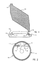
- FIG. 2 is an end view of the preferred embodiment roller 110 with the preferred embodiment pad 100 held firmly in place.
- the roller has clamping means 112 disposed at opposite ends, for securely holding the cleaning pad 100 in place on the roller 110 and further includes driving means 114 for rotatably driving the roller.
- the clamping means 112 on the preferred embodiment roller 110 is a lever 116 mounted in a notch 118.
- the notch 118 forms a shelf 120 on which the lever 116 is mounted.
- the lever 116 clamps a pad tab 102 to the shelf 120, firmly holding the clamped tab 102 in place.
- the preferred lever 116 has a pivot 122 at one end and a serrated surface 124 for gripping the tab 102 at an opposite end.
- a clamping screw 126 locks the lever 116 firmly against the tab 102, which is thus clamped between the serrated surface 124 and the shelf 120.
- the clamping screw 126 passes through the lever 116 between the pivot 122 and the serrated surface 124 and enters the roller 110 in a threaded hole 128 in the shelf 120. So, screwing the clamping screw 126 into the shelf 120 tightens the grip of the clamping means 112 on the clamped tab 102.
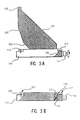
- the pad 100 is attached to the roller 110 by inserting one tab 102 into one of the clamping means 112; tightening the clamping screw 126 to clamp the inserted tab 102; wrapping the pad 100 in the intended direction of rotation in a helix-like fashion around the roller 110; and, in FIG. 3B, inserting and clamping the remaining tab 102 in the remaining clamping means 112.
- the pad edges 130, 132 do not overlap and are gapped from each other.
- the gap 134 channels used cleaning solution, debris, etc. away and off of the article being cleaned.
- FIG. 4B which is an expanded view of the first cleaning station 146 and is typical for both cleaning stations 150 and 152
- cleaning solution 160 drops onto the cleaning pad and roller assembly 142.
- the wafer 146' being cleaned passes between a support roller 162 and the cleaning pad/roller assembly 142.
- the cleaning pad/roller assembly 142 acts to provide fresh cleaning solution to the wafer 146', while simultaneously removing spent, contaminated cleaning solution and debris.
Landscapes
- Cleaning Or Drying Semiconductors (AREA)
- Cleaning In General (AREA)
- Coating Apparatus (AREA)
Applications Claiming Priority (2)
| Application Number | Priority Date | Filing Date | Title |
|---|---|---|---|
| US08/686,048 US5813082A (en) | 1996-07-24 | 1996-07-24 | Pad and roller assembly for cleaning semiconductor wafers |
| US686048 | 1996-07-24 |
Publications (2)
| Publication Number | Publication Date |
|---|---|
| EP0821402A2 true EP0821402A2 (de) | 1998-01-28 |
| EP0821402A3 EP0821402A3 (de) | 2002-05-22 |
Family
ID=24754688
Family Applications (1)
| Application Number | Title | Priority Date | Filing Date |
|---|---|---|---|
| EP97304741A Withdrawn EP0821402A3 (de) | 1996-07-24 | 1997-07-01 | Anordnung von Träger und Rolle |
Country Status (3)
| Country | Link |
|---|---|
| US (2) | US5813082A (de) |
| EP (1) | EP0821402A3 (de) |
| JP (1) | JP3105827B2 (de) |
Cited By (1)
| Publication number | Priority date | Publication date | Assignee | Title |
|---|---|---|---|---|
| EP0993023A1 (de) * | 1998-10-05 | 2000-04-12 | Agfa-Gevaert N.V. | Verfahren zur Übertragung eines bahn- oder blattförmigen Materials in einem Reinraum |
Families Citing this family (6)
| Publication number | Priority date | Publication date | Assignee | Title |
|---|---|---|---|---|
| EP0831512A4 (de) | 1995-06-09 | 1999-02-10 | Toshiba Kk | Vorratskathodenstruktur, kathodensubstrat für diese stuktur, elektronenkanonenstruktur unter verwendung dieser struktur und elektronenröhre |
| US5813082A (en) * | 1996-07-24 | 1998-09-29 | International Business Machines Corporation | Pad and roller assembly for cleaning semiconductor wafers |
| IL123707A (en) * | 1997-05-26 | 2001-01-28 | Heidelberger Druckmasch Ag | Method and device for eliminating peeled-off surface portions of an ink-repellent layer of an offset printing plate |
| US6951044B2 (en) | 2002-02-09 | 2005-10-04 | Kaim Wayne K | Paper cleaning buff |
| US7481829B2 (en) * | 2003-04-21 | 2009-01-27 | Atlas Spine, Inc. | Bone fixation plate |
| US6920796B2 (en) * | 2003-11-13 | 2005-07-26 | Nan Ya Technology Corporation | Device used for detecting clamping force of processed object and method thereof |
Family Cites Families (12)
| Publication number | Priority date | Publication date | Assignee | Title |
|---|---|---|---|---|
| US801003A (en) * | 1903-12-21 | 1905-10-03 | United Shoe Machinery Ab | Buffing or polishing roll. |
| US869572A (en) * | 1906-08-04 | 1907-10-29 | James H Hunt | Covering for mangle-rolls. |
| US2630657A (en) * | 1950-12-29 | 1953-03-10 | Earle L Harley | Strip material and means for applying same to rollers |
| US3234694A (en) * | 1963-11-06 | 1966-02-15 | John F Vosburg | Abrasive strip holding and tightening mechanism |
| US3610693A (en) * | 1969-12-30 | 1971-10-05 | Xerox Corp | Method of making a cylindrical brush |
| US3886622A (en) * | 1973-01-26 | 1975-06-03 | Western Sales & Supply Co | Tubular buffer element |
| JPS58182234A (ja) * | 1982-04-17 | 1983-10-25 | Dainippon Screen Mfg Co Ltd | 複数種のブラシ使用可能な洗浄装置 |
| ES283921Y (es) * | 1985-01-11 | 1986-06-16 | Alvarez Garcia Jaime | Dispositivo perfeccionado de enrollamiento helicoidal de cinta de tejido sobre tubos de plastico para rodillos de pintura |
| US4627127A (en) * | 1985-02-13 | 1986-12-09 | Minnesota Mining And Manufacturing Company | Cylindrical brush |
| US4947029A (en) * | 1985-11-01 | 1990-08-07 | Canon Kabushiki Kaisha | Cleaning device for information recording medium |
| GB8907969D0 (en) * | 1989-04-08 | 1989-05-24 | Holdsworth James & Brothers | Card clothing |
| US5813082A (en) * | 1996-07-24 | 1998-09-29 | International Business Machines Corporation | Pad and roller assembly for cleaning semiconductor wafers |
-
1996
- 1996-07-24 US US08/686,048 patent/US5813082A/en not_active Expired - Fee Related
-
1997
- 1997-06-23 JP JP09165682A patent/JP3105827B2/ja not_active Expired - Fee Related
- 1997-07-01 EP EP97304741A patent/EP0821402A3/de not_active Withdrawn
-
1998
- 1998-06-30 US US09/109,225 patent/US6125496A/en not_active Expired - Fee Related
Cited By (1)
| Publication number | Priority date | Publication date | Assignee | Title |
|---|---|---|---|---|
| EP0993023A1 (de) * | 1998-10-05 | 2000-04-12 | Agfa-Gevaert N.V. | Verfahren zur Übertragung eines bahn- oder blattförmigen Materials in einem Reinraum |
Also Published As
| Publication number | Publication date |
|---|---|
| JPH1083979A (ja) | 1998-03-31 |
| US6125496A (en) | 2000-10-03 |
| JP3105827B2 (ja) | 2000-11-06 |
| EP0821402A3 (de) | 2002-05-22 |
| US5813082A (en) | 1998-09-29 |
Similar Documents
| Publication | Publication Date | Title |
|---|---|---|
| US5868863A (en) | Method and apparatus for cleaning of semiconductor substrates using hydrofluoric acid (HF) | |
| US5813082A (en) | Pad and roller assembly for cleaning semiconductor wafers | |
| EP1661731A3 (de) | Verfahren zum Entfernen von Rückständen von einem Halbleitersubstrat | |
| EP1077474A2 (de) | Rückseite ätzen in einem Schrubber | |
| JP3626610B2 (ja) | 処理装置及び処理方法 | |
| KR20000035252A (ko) | 반도체 장치 제조 방법 | |
| JP2009543319A (ja) | 半導体ウェーハの洗浄方法 | |
| EP3573090B1 (de) | Verfahren zur halbleiterwaferreinigung | |
| JPH11283951A (ja) | 半導体ウエーハ等用洗浄装置 | |
| JPS63133534A (ja) | 半導体ウエハの洗浄方法 | |
| JP3194592B2 (ja) | 枚葉式ウェハー洗浄装置 | |
| JP2004063201A (ja) | 基板の処理装置 | |
| KR100202670B1 (ko) | 반도체 리드프레임의 도금방법 | |
| JPH09199462A (ja) | ウエハ洗浄方法及びそのための装置 | |
| JPH05160104A (ja) | 半導体ウェーハのウェット処理方法及びウェット処理装置 | |
| JP2001023942A (ja) | 半導体ウェハ上の集積回路デバイスの電解腐食を低減させる方法 | |
| CN101312114B (zh) | 浸入式湿法工艺中防止硅片背面沾污正面的方法 | |
| JP3271438B2 (ja) | 表面処理用部材、表面処理装置、表面処理方法、並びに、半導体装置の製造方法 | |
| JP3489329B2 (ja) | シリコンウエーハ表面の処理方法 | |
| JPS6227743B2 (de) | ||
| JPH05217988A (ja) | 洗浄装置 | |
| KR100583633B1 (ko) | 기판 반송 로봇 | |
| JP2001077072A (ja) | 基板の洗浄方法 | |
| JP2552731Y2 (ja) | 基板現像処理装置 | |
| JP3716456B2 (ja) | エッチング部品の製造方法 |
Legal Events
| Date | Code | Title | Description |
|---|---|---|---|
| PUAI | Public reference made under article 153(3) epc to a published international application that has entered the european phase |
Free format text: ORIGINAL CODE: 0009012 |
|
| AK | Designated contracting states |
Kind code of ref document: A2 Designated state(s): AT BE CH DE DK ES FI FR GB GR IE IT LI LU MC NL PT SE |
|
| PUAL | Search report despatched |
Free format text: ORIGINAL CODE: 0009013 |
|
| RIC1 | Information provided on ipc code assigned before grant |
Free format text: 7H 01L 21/00 A, 7B 08B 11/00 B, 7B 08B 1/04 B, 7A 46B 13/00 B |
|
| AKX | Designation fees paid | ||
| REG | Reference to a national code |
Ref country code: DE Ref legal event code: 8566 |
|
| STAA | Information on the status of an ep patent application or granted ep patent |
Free format text: STATUS: THE APPLICATION IS DEEMED TO BE WITHDRAWN |
|
| 18D | Application deemed to be withdrawn |
Effective date: 20021123 |