EP0810669A1 - Matrice de transistors à couches minces - Google Patents
Matrice de transistors à couches minces Download PDFInfo
- Publication number
- EP0810669A1 EP0810669A1 EP97108538A EP97108538A EP0810669A1 EP 0810669 A1 EP0810669 A1 EP 0810669A1 EP 97108538 A EP97108538 A EP 97108538A EP 97108538 A EP97108538 A EP 97108538A EP 0810669 A1 EP0810669 A1 EP 0810669A1
- Authority
- EP
- European Patent Office
- Prior art keywords
- thin film
- film transistor
- wires
- gate
- drain
- Prior art date
- Legal status (The legal status is an assumption and is not a legal conclusion. Google has not performed a legal analysis and makes no representation as to the accuracy of the status listed.)
- Withdrawn
Links
- 239000010409 thin film Substances 0.000 title claims abstract description 56
- 239000010408 film Substances 0.000 claims abstract description 184
- 239000004065 semiconductor Substances 0.000 claims abstract description 49
- 239000000758 substrate Substances 0.000 claims abstract description 25
- 239000003990 capacitor Substances 0.000 claims abstract description 11
- 239000011159 matrix material Substances 0.000 claims abstract description 8
- 239000000463 material Substances 0.000 claims abstract description 4
- 229910021417 amorphous silicon Inorganic materials 0.000 claims description 44
- 239000010410 layer Substances 0.000 claims description 32
- 239000004973 liquid crystal related substance Substances 0.000 claims description 21
- 125000006850 spacer group Chemical group 0.000 claims description 9
- OAICVXFJPJFONN-UHFFFAOYSA-N Phosphorus Chemical compound [P] OAICVXFJPJFONN-UHFFFAOYSA-N 0.000 claims description 3
- 229910052698 phosphorus Inorganic materials 0.000 claims description 3
- 239000011574 phosphorus Substances 0.000 claims description 3
- 239000004020 conductor Substances 0.000 claims 2
- 238000000034 method Methods 0.000 description 23
- 238000004519 manufacturing process Methods 0.000 description 20
- 229910052751 metal Inorganic materials 0.000 description 20
- 239000002184 metal Substances 0.000 description 20
- 230000008569 process Effects 0.000 description 19
- 238000000206 photolithography Methods 0.000 description 16
- 230000003071 parasitic effect Effects 0.000 description 7
- XUIMIQQOPSSXEZ-UHFFFAOYSA-N Silicon Chemical compound [Si] XUIMIQQOPSSXEZ-UHFFFAOYSA-N 0.000 description 6
- 229910052782 aluminium Inorganic materials 0.000 description 6
- XAGFODPZIPBFFR-UHFFFAOYSA-N aluminium Chemical compound [Al] XAGFODPZIPBFFR-UHFFFAOYSA-N 0.000 description 6
- 229910052710 silicon Inorganic materials 0.000 description 6
- 239000010703 silicon Substances 0.000 description 6
- 238000002955 isolation Methods 0.000 description 5
- 238000000926 separation method Methods 0.000 description 5
- VYZAMTAEIAYCRO-UHFFFAOYSA-N Chromium Chemical compound [Cr] VYZAMTAEIAYCRO-UHFFFAOYSA-N 0.000 description 4
- 229910052804 chromium Inorganic materials 0.000 description 4
- 239000011651 chromium Substances 0.000 description 4
- 238000010586 diagram Methods 0.000 description 4
- 238000004544 sputter deposition Methods 0.000 description 4
- 230000015572 biosynthetic process Effects 0.000 description 3
- 230000000452 restraining effect Effects 0.000 description 3
- 238000005229 chemical vapour deposition Methods 0.000 description 2
- 239000011521 glass Substances 0.000 description 2
- ZOKXTWBITQBERF-UHFFFAOYSA-N Molybdenum Chemical compound [Mo] ZOKXTWBITQBERF-UHFFFAOYSA-N 0.000 description 1
- 239000000956 alloy Substances 0.000 description 1
- 229910045601 alloy Inorganic materials 0.000 description 1
- 230000008859 change Effects 0.000 description 1
- AMGQUBHHOARCQH-UHFFFAOYSA-N indium;oxotin Chemical compound [In].[Sn]=O AMGQUBHHOARCQH-UHFFFAOYSA-N 0.000 description 1
- 229910052750 molybdenum Inorganic materials 0.000 description 1
- 239000011733 molybdenum Substances 0.000 description 1
- 238000009832 plasma treatment Methods 0.000 description 1
- 238000000623 plasma-assisted chemical vapour deposition Methods 0.000 description 1
- 230000009467 reduction Effects 0.000 description 1
- 230000002787 reinforcement Effects 0.000 description 1
- 239000002356 single layer Substances 0.000 description 1
- 229910052715 tantalum Inorganic materials 0.000 description 1
- GUVRBAGPIYLISA-UHFFFAOYSA-N tantalum atom Chemical compound [Ta] GUVRBAGPIYLISA-UHFFFAOYSA-N 0.000 description 1
- WFKWXMTUELFFGS-UHFFFAOYSA-N tungsten Chemical compound [W] WFKWXMTUELFFGS-UHFFFAOYSA-N 0.000 description 1
- 229910052721 tungsten Inorganic materials 0.000 description 1
- 239000010937 tungsten Substances 0.000 description 1
Images


Classifications
-
- G—PHYSICS
- G02—OPTICS
- G02F—OPTICAL DEVICES OR ARRANGEMENTS FOR THE CONTROL OF LIGHT BY MODIFICATION OF THE OPTICAL PROPERTIES OF THE MEDIA OF THE ELEMENTS INVOLVED THEREIN; NON-LINEAR OPTICS; FREQUENCY-CHANGING OF LIGHT; OPTICAL LOGIC ELEMENTS; OPTICAL ANALOGUE/DIGITAL CONVERTERS
- G02F1/00—Devices or arrangements for the control of the intensity, colour, phase, polarisation or direction of light arriving from an independent light source, e.g. switching, gating or modulating; Non-linear optics
- G02F1/01—Devices or arrangements for the control of the intensity, colour, phase, polarisation or direction of light arriving from an independent light source, e.g. switching, gating or modulating; Non-linear optics for the control of the intensity, phase, polarisation or colour
- G02F1/13—Devices or arrangements for the control of the intensity, colour, phase, polarisation or direction of light arriving from an independent light source, e.g. switching, gating or modulating; Non-linear optics for the control of the intensity, phase, polarisation or colour based on liquid crystals, e.g. single liquid crystal display cells
- G02F1/133—Constructional arrangements; Operation of liquid crystal cells; Circuit arrangements
- G02F1/136—Liquid crystal cells structurally associated with a semi-conducting layer or substrate, e.g. cells forming part of an integrated circuit
- G02F1/1362—Active matrix addressed cells
- G02F1/136213—Storage capacitors associated with the pixel electrode
-
- H—ELECTRICITY
- H01—ELECTRIC ELEMENTS
- H01L—SEMICONDUCTOR DEVICES NOT COVERED BY CLASS H10
- H01L27/00—Devices consisting of a plurality of semiconductor or other solid-state components formed in or on a common substrate
- H01L27/02—Devices consisting of a plurality of semiconductor or other solid-state components formed in or on a common substrate including semiconductor components specially adapted for rectifying, oscillating, amplifying or switching and having at least one potential-jump barrier or surface barrier; including integrated passive circuit elements with at least one potential-jump barrier or surface barrier
- H01L27/12—Devices consisting of a plurality of semiconductor or other solid-state components formed in or on a common substrate including semiconductor components specially adapted for rectifying, oscillating, amplifying or switching and having at least one potential-jump barrier or surface barrier; including integrated passive circuit elements with at least one potential-jump barrier or surface barrier the substrate being other than a semiconductor body, e.g. an insulating body
- H01L27/1214—Devices consisting of a plurality of semiconductor or other solid-state components formed in or on a common substrate including semiconductor components specially adapted for rectifying, oscillating, amplifying or switching and having at least one potential-jump barrier or surface barrier; including integrated passive circuit elements with at least one potential-jump barrier or surface barrier the substrate being other than a semiconductor body, e.g. an insulating body comprising a plurality of TFTs formed on a non-semiconducting substrate, e.g. driving circuits for AMLCDs
- H01L27/1259—Multistep manufacturing methods
- H01L27/1288—Multistep manufacturing methods employing particular masking sequences or specially adapted masks, e.g. half-tone mask
-
- G—PHYSICS
- G02—OPTICS
- G02F—OPTICAL DEVICES OR ARRANGEMENTS FOR THE CONTROL OF LIGHT BY MODIFICATION OF THE OPTICAL PROPERTIES OF THE MEDIA OF THE ELEMENTS INVOLVED THEREIN; NON-LINEAR OPTICS; FREQUENCY-CHANGING OF LIGHT; OPTICAL LOGIC ELEMENTS; OPTICAL ANALOGUE/DIGITAL CONVERTERS
- G02F1/00—Devices or arrangements for the control of the intensity, colour, phase, polarisation or direction of light arriving from an independent light source, e.g. switching, gating or modulating; Non-linear optics
- G02F1/01—Devices or arrangements for the control of the intensity, colour, phase, polarisation or direction of light arriving from an independent light source, e.g. switching, gating or modulating; Non-linear optics for the control of the intensity, phase, polarisation or colour
- G02F1/13—Devices or arrangements for the control of the intensity, colour, phase, polarisation or direction of light arriving from an independent light source, e.g. switching, gating or modulating; Non-linear optics for the control of the intensity, phase, polarisation or colour based on liquid crystals, e.g. single liquid crystal display cells
- G02F1/133—Constructional arrangements; Operation of liquid crystal cells; Circuit arrangements
- G02F1/1333—Constructional arrangements; Manufacturing methods
- G02F1/1339—Gaskets; Spacers; Sealing of cells
-
- G—PHYSICS
- G02—OPTICS
- G02F—OPTICAL DEVICES OR ARRANGEMENTS FOR THE CONTROL OF LIGHT BY MODIFICATION OF THE OPTICAL PROPERTIES OF THE MEDIA OF THE ELEMENTS INVOLVED THEREIN; NON-LINEAR OPTICS; FREQUENCY-CHANGING OF LIGHT; OPTICAL LOGIC ELEMENTS; OPTICAL ANALOGUE/DIGITAL CONVERTERS
- G02F1/00—Devices or arrangements for the control of the intensity, colour, phase, polarisation or direction of light arriving from an independent light source, e.g. switching, gating or modulating; Non-linear optics
- G02F1/01—Devices or arrangements for the control of the intensity, colour, phase, polarisation or direction of light arriving from an independent light source, e.g. switching, gating or modulating; Non-linear optics for the control of the intensity, phase, polarisation or colour
- G02F1/13—Devices or arrangements for the control of the intensity, colour, phase, polarisation or direction of light arriving from an independent light source, e.g. switching, gating or modulating; Non-linear optics for the control of the intensity, phase, polarisation or colour based on liquid crystals, e.g. single liquid crystal display cells
- G02F1/133—Constructional arrangements; Operation of liquid crystal cells; Circuit arrangements
- G02F1/1333—Constructional arrangements; Manufacturing methods
- G02F1/1343—Electrodes
- G02F1/134309—Electrodes characterised by their geometrical arrangement
- G02F1/134363—Electrodes characterised by their geometrical arrangement for applying an electric field parallel to the substrate, i.e. in-plane switching [IPS]
-
- G—PHYSICS
- G02—OPTICS
- G02F—OPTICAL DEVICES OR ARRANGEMENTS FOR THE CONTROL OF LIGHT BY MODIFICATION OF THE OPTICAL PROPERTIES OF THE MEDIA OF THE ELEMENTS INVOLVED THEREIN; NON-LINEAR OPTICS; FREQUENCY-CHANGING OF LIGHT; OPTICAL LOGIC ELEMENTS; OPTICAL ANALOGUE/DIGITAL CONVERTERS
- G02F1/00—Devices or arrangements for the control of the intensity, colour, phase, polarisation or direction of light arriving from an independent light source, e.g. switching, gating or modulating; Non-linear optics
- G02F1/01—Devices or arrangements for the control of the intensity, colour, phase, polarisation or direction of light arriving from an independent light source, e.g. switching, gating or modulating; Non-linear optics for the control of the intensity, phase, polarisation or colour
- G02F1/13—Devices or arrangements for the control of the intensity, colour, phase, polarisation or direction of light arriving from an independent light source, e.g. switching, gating or modulating; Non-linear optics for the control of the intensity, phase, polarisation or colour based on liquid crystals, e.g. single liquid crystal display cells
- G02F1/133—Constructional arrangements; Operation of liquid crystal cells; Circuit arrangements
- G02F1/136—Liquid crystal cells structurally associated with a semi-conducting layer or substrate, e.g. cells forming part of an integrated circuit
- G02F1/1362—Active matrix addressed cells
- G02F1/1368—Active matrix addressed cells in which the switching element is a three-electrode device
-
- H—ELECTRICITY
- H01—ELECTRIC ELEMENTS
- H01L—SEMICONDUCTOR DEVICES NOT COVERED BY CLASS H10
- H01L27/00—Devices consisting of a plurality of semiconductor or other solid-state components formed in or on a common substrate
- H01L27/02—Devices consisting of a plurality of semiconductor or other solid-state components formed in or on a common substrate including semiconductor components specially adapted for rectifying, oscillating, amplifying or switching and having at least one potential-jump barrier or surface barrier; including integrated passive circuit elements with at least one potential-jump barrier or surface barrier
- H01L27/12—Devices consisting of a plurality of semiconductor or other solid-state components formed in or on a common substrate including semiconductor components specially adapted for rectifying, oscillating, amplifying or switching and having at least one potential-jump barrier or surface barrier; including integrated passive circuit elements with at least one potential-jump barrier or surface barrier the substrate being other than a semiconductor body, e.g. an insulating body
- H01L27/1214—Devices consisting of a plurality of semiconductor or other solid-state components formed in or on a common substrate including semiconductor components specially adapted for rectifying, oscillating, amplifying or switching and having at least one potential-jump barrier or surface barrier; including integrated passive circuit elements with at least one potential-jump barrier or surface barrier the substrate being other than a semiconductor body, e.g. an insulating body comprising a plurality of TFTs formed on a non-semiconducting substrate, e.g. driving circuits for AMLCDs
- H01L27/124—Devices consisting of a plurality of semiconductor or other solid-state components formed in or on a common substrate including semiconductor components specially adapted for rectifying, oscillating, amplifying or switching and having at least one potential-jump barrier or surface barrier; including integrated passive circuit elements with at least one potential-jump barrier or surface barrier the substrate being other than a semiconductor body, e.g. an insulating body comprising a plurality of TFTs formed on a non-semiconducting substrate, e.g. driving circuits for AMLCDs with a particular composition, shape or layout of the wiring layers specially adapted to the circuit arrangement, e.g. scanning lines in LCD pixel circuits
-
- H—ELECTRICITY
- H01—ELECTRIC ELEMENTS
- H01L—SEMICONDUCTOR DEVICES NOT COVERED BY CLASS H10
- H01L27/00—Devices consisting of a plurality of semiconductor or other solid-state components formed in or on a common substrate
- H01L27/02—Devices consisting of a plurality of semiconductor or other solid-state components formed in or on a common substrate including semiconductor components specially adapted for rectifying, oscillating, amplifying or switching and having at least one potential-jump barrier or surface barrier; including integrated passive circuit elements with at least one potential-jump barrier or surface barrier
- H01L27/12—Devices consisting of a plurality of semiconductor or other solid-state components formed in or on a common substrate including semiconductor components specially adapted for rectifying, oscillating, amplifying or switching and having at least one potential-jump barrier or surface barrier; including integrated passive circuit elements with at least one potential-jump barrier or surface barrier the substrate being other than a semiconductor body, e.g. an insulating body
- H01L27/1214—Devices consisting of a plurality of semiconductor or other solid-state components formed in or on a common substrate including semiconductor components specially adapted for rectifying, oscillating, amplifying or switching and having at least one potential-jump barrier or surface barrier; including integrated passive circuit elements with at least one potential-jump barrier or surface barrier the substrate being other than a semiconductor body, e.g. an insulating body comprising a plurality of TFTs formed on a non-semiconducting substrate, e.g. driving circuits for AMLCDs
- H01L27/1255—Devices consisting of a plurality of semiconductor or other solid-state components formed in or on a common substrate including semiconductor components specially adapted for rectifying, oscillating, amplifying or switching and having at least one potential-jump barrier or surface barrier; including integrated passive circuit elements with at least one potential-jump barrier or surface barrier the substrate being other than a semiconductor body, e.g. an insulating body comprising a plurality of TFTs formed on a non-semiconducting substrate, e.g. driving circuits for AMLCDs integrated with passive devices, e.g. auxiliary capacitors
Definitions
- the present invention relates to a thin film transistor element array disposed on an insulating substrate, and more specifically, it relates to the thin film transistor element array having a wire electrode suitable for being used for an active matrix type liquid crystal display.
- the demand of the liquid crystal display has risen. More specifically, since the active matrix type liquid crystal display wherein the thin film transistor is disposed as a switch of each pixel on one glass substrate has a high quality image, more and more demand is growing. In order that such a liquid crystal display may be developed henceforth, the reduction of cost is a critical problem. A manufacturing process is required to be simplified. In an example of the prior art relating to the simplification of a photolithography process, there is disclosed the active matrix type liquid crystal display by the use of the thin film transistor element whose structure can be formed by means of two-time photolithography process.
- FIGs. 1A, 1B and 1C are a plan view and a cross sectional view showing the structure of the thin film transistor, a first conventional example used for the active matrix type liquid crystal display, which can be manufactured by means of two-time photolithography process (Japanese Patent National Publication (Kohyo) No. 501562/1984).
- a portion A-A functions as the thin film transistor.
- An ITO (Indium Tin Oxide) film 21 functions as a signal wire.
- a metal film 6 functions as a control wire.
- An ITO film 22 functions as a pixel electrode.
- a laminated film of the ITO film and an n + amorphous silicon film are sequentially formed on a transmittable insulating substrate 1. After the photolithography process, a pattern is formed. Next, the laminated film of an amorphous silicon semiconductor film 4, an insulating film 5 and the metal film 6 is formed. After the photolithography process, the pattern is formed. At this time, an n + amorphous silicon film 3 on the ITO films 21, 22 is also removed. Although six to seven mask patterns are normally necessary, in case of the conventional example, the thin film transistor element array is formed by two-time photolithography process.
- FIGs. 2A, 2B and 2C are a plan view and a cross sectional view to describe the second conventional example.
- the manufacturing process of the second conventional example is the same as the first conventional example up to the formation of metal films 61 and 62.
- the laminated film pattern of the n + amorphous silicon film 3, the amorphous silicon semiconductor film 4, the insulating film 5 and the metal film 62 is left on one part of the ITO film 21, isolating from the thin film transistor element comprising the laminated film pattern of the amorphous silicon semiconductor film 4, the insulating film 5 and the metal film 61.
- the structure of a signal wire portion is the laminated structure of the ITO film 21, the n + amorphous silicon film 3, the amorphous silicon semiconductor film 4, the insulating film 5 and the metal film 61. Therefore, even if disconnection arises on the ITO film 21, an electrical connection is held by the n + amorphous silicon film 3.
- FIGs. 3A, 3B and 3C show the structure of a third conventional example which is intended to reduce a resistance of a drain wire.
- a first metal film 10 is disposed on the ITO film 21, whereby the resistance of the drain wire is reduced.
- the manufacturing method of the conventional example is the same as the first conventional example up to the formation of the pattern of the ITO films 21, 22 and the n + amorphous silicon film 3.
- the pattern of the first metal film 10 is formed.
- the method is the same as the first conventional example from the formation of the amorphous silicon semiconductor film 4. Accordingly, the resistance of the drain wire can be reduced by means of three-time photolithography process.
- the resistance of the signal wire is very high. Accordingly, in case that the examples are applied to a liquid crystal display device having a large screen, there is such a problem that correct images cannot be carried out due to a drain signal delay at a position separated from a signal input terminal.
- the signal wire comprises a single layer of the ITO film 21 having a high resistivity.
- the second conventional example it is the laminated film of the ITO film 21 and the n + amorphous silicon film 3 that electrically contributes among the laminated films constituting the signal wire. Accordingly, in both the example, the signal wire has the high resistivity.
- Another problem of the first, second third conventional examples is as follows. Since a leakage current flows between the pixel electrode and an adjacent drain electrode wire, a voltage applied to the pixel is dropped, whereby the display of the liquid crystal display is not normal. The reason is that the laminated structure of the amorphous silicon semiconductor film 4, the insulating film 5 and the metal portion 61 is all over the area of a gate electrode wire whereby a parasitic transistor exists between the pixel electrode and the adjacent drain electrode wire.
- an auxiliary capacitance for restraining a change in an electric potential of the pixel electrode cannot be formed.
- the reason is as follows.
- the pixel electrode, that is, the ITO film 22 is overlapped with the one line previous gate electrode wire.
- the leakage current flows between the pixel electrode and the drain electrode wire via the parasitic transistor described above, whereby it is difficult to normally hold a pixel potential.
- a thin film transistor element array comprises a plurality of thin film transistor elements disposed over a substrate in a matrix including a plurality of rows and columns, each of the thin film transistor elements including a source electrode, a drain electrode, a first laminated layer of a first semiconductor layer and a first gate insulating film, and a gate electrode formed on the first laminated layer, the first laminated layer being provided in island form; a plurality of drain wires provided over the substrate, each of the drain wires being elongated to be connected to the drain electrode of each of the thin film transistor elements disposed in an associated one of the columns; a plurality of gate wires provided over the substrate, each of the gate wires being elongated to be connected to the gate electrode of each transistor elements disposed in an associated one of the rows; a plurality of spacers each provided in island form, each of the spacers being provided at an associated one of intersections of the gate wires and the drain wires so as to insulate each of the gate wires
- a thin film transistor element array further comprises each of a plurality of pixel electrodes provided over the substrate to be connected to the source electrode, each of pixel electrodes having a overlapping section with adjacent one of the gate wires; and a plurality of auxiliary capacitors including a third laminated layer of a third semiconductor layer and a third gate insulating film, and the third laminated layer being provided in island form.
- the thin film transistor element array according to the present invention is provided with a metal film which is directly disposed on the drain electrode wire. Accordingly, a drain wire resistance is low, so that the delay time of the drain signal is short.
- a pattern of an amorphous silicon semiconductor film at the transistor portion is isolated. Accordingly, a parasitic transistor does not exist between the pixel electrode and the adjacent drain electrode, whereby the leakage current do not flow between them.
- the pattern of the amorphous silicon semiconductor film which exists in the overlapping portion of the pixel electrode with the previous line of gate electrode wires is also isolated. Accordingly, it is possible to form an auxiliary capacitor so as not to generates the leakage current between the adjacent drain electrode wire and the auxiliary capacitance.
- a liquid crystal display used for a thin film transistor element array of the present invention is described.
- Fig. 8 is a schematic diagram of the liquid crystal display.
- the liquid crystal display is provided with a V-driver for vertically scanning at the side of a display portion 12 and an H-driver for horizontally supplying image signals above or under the display portion 12.
- Fig. 9 is a circuit diagram of the thin film transistor element array used for the display portion 12. The array is provided with a plurality of horizontally elongating gate electrode wires and a plurality of vertically elongating drain electrode wires.
- the gate electrode wires and the drain electrode wires are connected to the V-driver and the H-driver, respectively.
- the array has display electrodes 18 in the portion surrounded by the gate electrode wires and the drain electrode wires of the array. Electric charges are supplied to the display electrodes 18 via a thin film transistor element 15.
- a common electrode 19 is disposed on a opposed substrate (not shown) which is coupled with the substrate where the array is formed.
- a liquid crystal capacitor 17 is disposed between the display electrode 18 and the common electrode 19. According to the present invention, since an auxiliary capacitor 16 is formed between the a previous line of gate electrode wires, a capability for holding the electric charge is improved.
- the thin film transistor element array of the present invention is applied to the liquid crystal display as described above, the application is not restricted to this example. Henceforth, the thin film transistor element array according to the present invention will described.
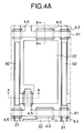
- FIG. 4A is a plan view to describe a first embodiment according to the present invention.
- FIGs. 4A and 4B are cross sectional views taken on line A-A and line B-B of FIG. 4A, respectively.
- the drain electrode wires comprising an ITO film 21 having a thickness of approximately 50 nm and a pixel electrode comprising an ITO film 22 are formed on a transmittable insulating substrate 1 such as a glass.
- the drain electrode wire has a width of approximately 10 ⁇ m.
- An islandlike-laminated film of an amorphous silicon semiconductor film 4 having the thickness of approximately 50 nm and an insulating film 5 having the thickness of approximately 300 nm is disposed between the ITO film 21 and the ITO film 22.
- the laminated film is formed in isolation.
- n + amorphous silicon film 3 having the thickness of approximately 10 nm is formed in a contact portion of the ITO films 21, 22 with the amorphous silicon semiconductor film 4.
- a metal film 61 is formed on the insulating film 5.
- the thin film transistor comprises the ITO films 21, 22, the n + amorphous silicon film 3, the amorphous silicon semiconductor film 4, the insulating film 5 and the metal film 61.
- the thin film transistor is constituted in such a manner that a leakage current does not flow between the pixel electrode and the adjacent drain electrode wire. Furthermore, the adjacent gate electrode wire and the pixel electrode have an overlapping section with each other.
- the islandlike-pattern of the laminated film of the n + amorphous semiconductor film 3, the amorphous silicon semiconductor film 4 and the insulating film 5 is disposed in isolation between the pixel electrode and the gate electrode wire in the overlapping section. This part functions as the auxiliary capacitor for restraining a potential of the pixel electrode from dropping.
- the islandlike pattern of the laminated film is disposed in isolation, the leakage current does not flow between the auxiliary capacitance and the adjacent drain electrode wire.
- the amorphous silicon semiconductor film 4 and the insulating film 5 are also disposed, in isolation, like island form between the drain electrode wire and the gate electrode wire in the intersection of the gate electrode wire and the drain electrode wire.
- the amorphous silicon semiconductor film 4 and the insulating film 5 function as a insulating film.
- a metal film 62 having a low resistance is directly formed on the ITO film 21 to be in contact with the drain electrode wire. Therefore, since a wire resistance of the drain electrode wire is reduced, a signal delay can be reduced.
- the thin film transistor element array of the first embodiment is provided with the auxiliary capacitor between the a previous line of gate electrode wires and the pixel electrode (ITO film), the reliability is high. Since the parasitic transistor does not exist, the leakage current does not flow between the auxiliary capacitance and the drain electrode wire, and between the pixel electrode and the adjacent drain electrode wire. Moreover, the wire resistance of the drain electrode wire can be reduced. Accordingly, the structure of the first embodiment is suitable for enlarging the screen of the liquid crystal display. Furthermore, the high reliability can be obtained.
- FIGs. 5A to 5I are a plan view or a cross sectional view to describe a manufacturing process according to the first embodiment, respectively.
- the approximately 50 nm ITO film is formed on the transmittable insulating substrate 1 by means of a sputtering method.
- the approximately 10 nm n + amorphous silicon film 3 is formed by means of a CVD method.
- the drain electrode wire pattern and the pixel electrode pattern are formed.
- the drain electrode wire pattern and the pixel electrode pattern are a laminated structure of the ITO films 21, 22 and the n + amorphous silicon film 3.
- the approximately 50 nm amorphous silicon semiconductor film 4 and an approximately 300 nm silicon nitrided film 7 are formed by means of the CVD method.
- the laminated film pattern of the semiconductor layer and the gate insulating film, the capacitance insulating film pattern of the auxiliary capacitance formed between the pixel electrode and the gate electrode wire, and the interlaminar separation insulating film pattern in the crossing portion of the drain electrode wire and the gate electrode wire are formed at a time. All the laminated film pattern, the capacitance insulating film pattern and the interlaminar separation insulating film pattern includes the laminated film pattern of the amorphous silicon semiconductor film 4 and the silicon nitrided film 7.
- an approximately 200 nm chromium film is formed by means of the sputtering method.
- the usual photolithography process is carried out.
- the gate electrode wire pattern comprising a chromium film 81 is formed, and, at the same time, the pattern having a remaining chromium film 82 is also formed on the drain electrode wire.
- the manufacturing method described above it is possible to achieve the thin film transistor element array having the auxiliary capacitance between the a previous line of gate electrode wires and the pixel electrode (ITO film) wherein the leakage current does not flow between the auxiliary capacitance and the drain electrode wire and between the pixel electrode and the adjacent drain electrode wire, and the wire resistance of the drain electrode wire is lower enough.
- the laminated film pattern of the semiconductor layer of the thin film transistor and the gate insulating film, the capacitance insulating film pattern of the auxiliary capacitance and the interlaminar separation insulating film pattern can be formed at the same time.
- the gate electrode wire pattern and the pattern which reduces the resistance of the drain electrode wire can be formed at the same time. Therefore, only three photolithography processes are required to be carried out. Accordingly, the manufacturing method is greatly amplified.
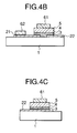
- FIGs. 6A, 6B and 6C are a plan view and a cross sectional view to describe a second embodiment according to the present invention.
- the difference between the first and second embodiments is that the n + amorphous silicon film 3 is formed all over the area on the lower side of the amorphous silicon semiconcudtor film 4.
- the n + amorphous silicon film 3 is only formed on the upper side of the ITO film 2.
- the n + amorphous silicon film 3 has a very thin thickness of approximately 1 nm. An off resistance of the transistor can be maintained to be high.
- the thin film transistor element array according to the second embodiment has the auxiliary capacitance between the a previous line of gate electrode wires and the pixel electrode (ITO film). The leakage current does not flow between the auxiliary capacitance and the drain electrode, and between the pixel electrode and the adjacent drain electrode wire.
- FIGs. 7A to 7I are a plan view and a cross sectional view to describe the manufacturing process according to the second embodiment.
- the approximately 50 nm ITO film is formed on the transmittable insulating substrate 1 by the sputtering method.
- the drain electrode wire pattern comprising the ITO film 21 and the pixel electrode pattern comprising the ITO film 22 are formed.
- a plasma treatment is performed with PH 3 gas added into Ar gas by the Plasma Enhanced CVD method, and phosphorus is doped all over the surface.
- the approximately 50 nm amorphous silicon semiconductor film 4 and the approximately 30 nm silicon nitrided film 7 are deposited, so that the phosphorus is diffused into the amorphous silicon semiconductor film 4.
- the laminated film of the n + amorphous silicon film 3, the amorphous silicon semi-conductor film 4 and the silicon nitrided film 7 are formed.
- the laminated film pattern of the n + amorphous silicon film 3 of the transistor, the amorphous silicon semiconductor film 4 and the silicon nitrided film 7, that is, the gate insulating film, and the insulating film pattern of the auxiliary capacitance formed between the pixel electrode and the gate electrode wire, and the interlaminar separation insulating film pattern at the intersection of the drain electrode wire and the gate electrode wire are formed at the same time.
- the approximately 10 nm aluminum film is formed by means of the sputtering method.
- the gate electrode pattern made of the aluminum film 91 is formed, and, at the same time, the pattern having the remaining aluminum film 92 is also formed on the drain electrode wire.
- the thin film transistor element array shown in FIGs. 6A, 6B and 6C can be achieved.
- the manufacturing method of the second embodiment similarly to the first embodiment, only three photolithography processes is required.
- a growth process of the n + amorphous silicon film is independently required, however, according to the manufacturing method of the second embodiment, it is possible to continuously deposite the n + amorphous silicon film 3, the amorphous silicon semiconductor film 4 and the silicon nitrided film 7 by a series of CVD process. That is to say, according to the second embodiment, it can be less CVD process by one time than the manufacturing method of the first embodiment. Accordingly, the manufacturing method can be further simplified.
- the gate metal film is the chromium film or the aluminum film.
- the metal film of the present invention is not restricted to the two kinds of films.
- a tantalum film, a molybdenum film, a tungsten film or various alloy films are suitable for the metal film.
- the wire resistance of the drain electrode wire can be lower enough, and the signal delay time can be reduced. Accordingly, even if the size of the screen is enlarged, normal images can be obtained on the liquid crystal display apparatus.
- one part of the drain electrode wire comprises the laminated structure of the ITO film and the gate metal film whereby the wire resistance of the drain electrode wire is low since the drain electrode wire is supported by the gate metal film.
- the leakage current does not flow between the pixel electrode and the adjacent drain electrode wire. Accordingly, a normal electric potential can be given into the pixel, and the liquid crystal display apparatus can normally display images. The reason is that the parasitic transistor does not exist between the pixel electrode and the adjacent drain electrode wire.
- the auxiliary capacitor for restraining changes from dropping in electric the pixel electrode can be disposed.
- the liquid crystal display apparatus having a high reliability can be provided.
- the reason is that the parasitic transistor does not exist between the auxiliary capacitance and the drain electrode wire.
- the simplified manufacturing process can be used, a manufacturing cost can be reduced.
- the reason is that the laminated film pattern of the semiconductor layer of the thin film transistor and the gate insulating film, the capacitance insulating film pattern of the auxiliary capacitance and the interlaminar separation insulating film pattern can be formed at the same time.
- the further reason is that the gate electrode wire and the electrode pattern which reduces the resistance of the drain electrode wire can be formed at the same time.
Applications Claiming Priority (2)
| Application Number | Priority Date | Filing Date | Title |
|---|---|---|---|
| JP13715396A JPH09318975A (ja) | 1996-05-30 | 1996-05-30 | 薄膜電界効果型トランジスタ素子アレイおよびその製造 方法 |
| JP137153/96 | 1996-05-30 |
Publications (1)
| Publication Number | Publication Date |
|---|---|
| EP0810669A1 true EP0810669A1 (fr) | 1997-12-03 |
Family
ID=15192069
Family Applications (1)
| Application Number | Title | Priority Date | Filing Date |
|---|---|---|---|
| EP97108538A Withdrawn EP0810669A1 (fr) | 1996-05-30 | 1997-05-27 | Matrice de transistors à couches minces |
Country Status (5)
| Country | Link |
|---|---|
| US (1) | US5952675A (fr) |
| EP (1) | EP0810669A1 (fr) |
| JP (1) | JPH09318975A (fr) |
| KR (1) | KR970076021A (fr) |
| TW (1) | TW343324B (fr) |
Cited By (5)
| Publication number | Priority date | Publication date | Assignee | Title |
|---|---|---|---|---|
| EP1168451A2 (fr) * | 2000-06-27 | 2002-01-02 | Canon Kabushiki Kaisha | Dispositif semi-conducteur, dispositif de détection de rayonnement et système dedétection de rayonnement utilisant un tel dispositif |
| EP1715531A1 (fr) * | 2005-04-22 | 2006-10-25 | Samsung SDI Co., Ltd. | Transistor à couche mince et écran plat l'utilisant |
| US8013346B2 (en) | 2000-12-21 | 2011-09-06 | Semiconductor Energy Laboratory Co., Ltd. | Light emitting device and method of manufacturing the same |
| US8421135B2 (en) | 2000-12-11 | 2013-04-16 | Semiconductor Energy Laboratory Co., Ltd. | Semiconductor device, and manufacturing method thereof |
| US11233132B2 (en) | 2009-03-05 | 2022-01-25 | Semiconductor Energy Laboratory Co., Ltd. | Semiconductor device |
Families Citing this family (9)
| Publication number | Priority date | Publication date | Assignee | Title |
|---|---|---|---|---|
| US6232208B1 (en) * | 1998-11-06 | 2001-05-15 | Advanced Micro Devices, Inc. | Semiconductor device and method of manufacturing a semiconductor device having an improved gate electrode profile |
| JP4067819B2 (ja) * | 2000-12-21 | 2008-03-26 | 株式会社半導体エネルギー研究所 | 発光装置 |
| JP2006303449A (ja) * | 2005-04-21 | 2006-11-02 | Samsung Sdi Co Ltd | アクティブマトリックス回路基板、この製造方法及びこれを備えたアクティブマトリックスディスプレイ装置 |
| TWI289360B (en) * | 2005-10-24 | 2007-11-01 | Chunghwa Picture Tubes Ltd | Thin film transistor array substrate and manufacturing method thereof |
| JP5111867B2 (ja) * | 2007-01-16 | 2013-01-09 | 株式会社ジャパンディスプレイイースト | 表示装置 |
| JP5305190B2 (ja) * | 2007-06-21 | 2013-10-02 | 株式会社ジャパンディスプレイ | 液晶表示装置 |
| DE102009007947B4 (de) * | 2009-02-06 | 2014-08-14 | Universität Stuttgart | Verfahren zur Herstellung eines Aktiv-Matrix-OLED-Displays |
| CN101819961B (zh) * | 2009-02-27 | 2015-04-29 | 北京京东方光电科技有限公司 | 液晶显示器的阵列基板、信号线及其制造方法 |
| CN107219702A (zh) * | 2017-07-20 | 2017-09-29 | 深圳市华星光电技术有限公司 | 一种阵列基板及其制造方法、液晶显示装置 |
Citations (4)
| Publication number | Priority date | Publication date | Assignee | Title |
|---|---|---|---|---|
| US4332075A (en) * | 1978-05-26 | 1982-06-01 | Matsushita Electric Industrial Co., Ltd. | Method of producing thin film transistor array |
| JPS60261174A (ja) * | 1984-06-07 | 1985-12-24 | Nippon Soken Inc | マトリツクスアレ− |
| EP0349255A2 (fr) * | 1988-07-01 | 1990-01-03 | Sharp Kabushiki Kaisha | Matrice de transistors à couche mince |
| EP0526076A1 (fr) * | 1991-07-24 | 1993-02-03 | Fujitsu Limited | Dispositif d'affichage à matrice active à cristaux liquides |
Family Cites Families (7)
| Publication number | Priority date | Publication date | Assignee | Title |
|---|---|---|---|---|
| FR2533072B1 (fr) * | 1982-09-14 | 1986-07-18 | Coissard Pierre | Procede de fabrication de circuits electroniques a base de transistors en couches minces et de condensateurs |
| WO1986002489A1 (fr) * | 1984-10-17 | 1986-04-24 | L'ETAT FRANCAIS représenté par LE MINISTRE DES PTT | Procede de fabrication de circuits electroniques a base de transistors en couches minces et de condensateurs |
| JP2703328B2 (ja) * | 1989-04-19 | 1998-01-26 | 三洋電機株式会社 | 液晶表示装置 |
| JP3089675B2 (ja) * | 1991-03-08 | 2000-09-18 | 日本電気株式会社 | 薄膜電界効果型トランジスタ駆動液晶表示素子アレイ及び駆動方法 |
| JPH06308511A (ja) * | 1993-04-26 | 1994-11-04 | Hitachi Ltd | 液晶表示基板 |
| JPH07110495A (ja) * | 1993-10-14 | 1995-04-25 | Hitachi Ltd | アクティブマトリクス型液晶表示装置 |
| JPH07325314A (ja) * | 1994-05-31 | 1995-12-12 | Sanyo Electric Co Ltd | 液晶表示装置 |
-
1996
- 1996-05-30 JP JP13715396A patent/JPH09318975A/ja active Pending
-
1997
- 1997-05-22 US US08/861,538 patent/US5952675A/en not_active Expired - Lifetime
- 1997-05-27 EP EP97108538A patent/EP0810669A1/fr not_active Withdrawn
- 1997-05-27 TW TW086107189A patent/TW343324B/zh not_active IP Right Cessation
- 1997-05-29 KR KR1019970021652A patent/KR970076021A/ko not_active Application Discontinuation
Patent Citations (4)
| Publication number | Priority date | Publication date | Assignee | Title |
|---|---|---|---|---|
| US4332075A (en) * | 1978-05-26 | 1982-06-01 | Matsushita Electric Industrial Co., Ltd. | Method of producing thin film transistor array |
| JPS60261174A (ja) * | 1984-06-07 | 1985-12-24 | Nippon Soken Inc | マトリツクスアレ− |
| EP0349255A2 (fr) * | 1988-07-01 | 1990-01-03 | Sharp Kabushiki Kaisha | Matrice de transistors à couche mince |
| EP0526076A1 (fr) * | 1991-07-24 | 1993-02-03 | Fujitsu Limited | Dispositif d'affichage à matrice active à cristaux liquides |
Non-Patent Citations (1)
| Title |
|---|
| PATENT ABSTRACTS OF JAPAN vol. 010, no. 129 (E - 403) 14 May 1986 (1986-05-14) * |
Cited By (14)
| Publication number | Priority date | Publication date | Assignee | Title |
|---|---|---|---|---|
| EP1168451A2 (fr) * | 2000-06-27 | 2002-01-02 | Canon Kabushiki Kaisha | Dispositif semi-conducteur, dispositif de détection de rayonnement et système dedétection de rayonnement utilisant un tel dispositif |
| EP1168451A3 (fr) * | 2000-06-27 | 2005-11-09 | Canon Kabushiki Kaisha | Dispositif semi-conducteur, dispositif de détection de rayonnement et système de détection de rayonnement utilisant un tel dispositif |
| US10665610B2 (en) | 2000-12-11 | 2020-05-26 | Semiconductor Energy Laboratory Co., Ltd. | Semiconductor device, and manufacturing method thereof |
| US9666601B2 (en) | 2000-12-11 | 2017-05-30 | Semiconductor Energy Laboratory Co., Ltd. | Semiconductor device, and manufacturing method thereof |
| US9059216B2 (en) | 2000-12-11 | 2015-06-16 | Semiconductor Energy Laboratory Co., Ltd. | Semiconductor device, and manufacturing method thereof |
| US8421135B2 (en) | 2000-12-11 | 2013-04-16 | Semiconductor Energy Laboratory Co., Ltd. | Semiconductor device, and manufacturing method thereof |
| US8735909B2 (en) | 2000-12-21 | 2014-05-27 | Semiconductor Energy Laboratory Co., Ltd. | Light emitting device and method of manufacturing the same |
| US8013346B2 (en) | 2000-12-21 | 2011-09-06 | Semiconductor Energy Laboratory Co., Ltd. | Light emitting device and method of manufacturing the same |
| US9231044B2 (en) | 2000-12-21 | 2016-01-05 | Semiconductor Energy Laboratory Co., Ltd. | Light emitting device and method of manufacturing the same |
| US9793335B2 (en) | 2000-12-21 | 2017-10-17 | Semiconductor Energy Laboratory Co., Ltd. | Light emitting device and method of manufacturing the same |
| US7550766B2 (en) | 2005-04-22 | 2009-06-23 | Samsung Mobile Display Co., Ltd. | Thin film transistor (TFT) and flat panel display including the TFT |
| EP1715531A1 (fr) * | 2005-04-22 | 2006-10-25 | Samsung SDI Co., Ltd. | Transistor à couche mince et écran plat l'utilisant |
| US11233132B2 (en) | 2009-03-05 | 2022-01-25 | Semiconductor Energy Laboratory Co., Ltd. | Semiconductor device |
| US11961894B2 (en) | 2009-03-05 | 2024-04-16 | Semiconductor Energy Laboratory Co., Ltd. | Semiconductor device |
Also Published As
| Publication number | Publication date |
|---|---|
| US5952675A (en) | 1999-09-14 |
| TW343324B (en) | 1998-10-21 |
| KR970076021A (ko) | 1997-12-10 |
| JPH09318975A (ja) | 1997-12-12 |
Similar Documents
| Publication | Publication Date | Title |
|---|---|---|
| US6566686B2 (en) | Thin-film transistor display devices | |
| US5828433A (en) | Liquid crystal display device and a method of manufacturing the same | |
| JP3307144B2 (ja) | 表示装置 | |
| EP0430592B1 (fr) | Dispositif d'affichage à matrice active | |
| JP4843719B2 (ja) | アレイ及び製品 | |
| EP0372821A2 (fr) | Panneau d'affichage à cristaux liquides avec réduction du nombre d'éléments d'image défectueux | |
| KR100260359B1 (ko) | 액정 표시 장치 및 그 제조방법 | |
| US4816885A (en) | Thin-film transistor matrix for liquid crystal display | |
| US5952675A (en) | Thin film transistor element array | |
| US5047819A (en) | Amorphous-silicon thin film transistor array substrate | |
| GB2275809A (en) | Liquid crystal display | |
| KR100268615B1 (ko) | 액티브매트릭스표시장치 | |
| EP0721215B1 (fr) | Fabrication d'une grille de lignes de balayage métalliques pour commander des lignes de portes en semiconducteur | |
| JP3657371B2 (ja) | アクティブマトリクス型表示装置 | |
| EP0721213B1 (fr) | Réseau de lignes de balayage métalliques pour commander des lignes de grilles en semi-conducteur | |
| EP0760966B1 (fr) | Architecture de matrice a grand diametre de spot pour afficheurs a cristaux liquides a matrice active | |
| KR100316072B1 (ko) | 액정 표시 장치 제조 방법 및 그 구조 | |
| JP3251401B2 (ja) | 半導体装置 | |
| JP3286843B2 (ja) | 液晶パネル | |
| US5877827A (en) | Liquid crystal display device having source electrode overlapping gate line | |
| KR0144233B1 (ko) | 액티브 매트릭스 방식의 액정 표시 장치 및 그의 제조 방법 | |
| JPH0568708B2 (fr) | ||
| JPH0572561A (ja) | アクテイブマトリクス基板 | |
| JP3466530B2 (ja) | 液晶表示装置およびそれに用いられる半導体装置の製造方法 | |
| JPH07159806A (ja) | アクティブマトリックス型液晶表示装置 |
Legal Events
| Date | Code | Title | Description |
|---|---|---|---|
| PUAI | Public reference made under article 153(3) epc to a published international application that has entered the european phase |
Free format text: ORIGINAL CODE: 0009012 |
|
| 17P | Request for examination filed |
Effective date: 19970903 |
|
| AK | Designated contracting states |
Kind code of ref document: A1 Designated state(s): DE FR GB |
|
| 17Q | First examination report despatched |
Effective date: 20011011 |
|
| STAA | Information on the status of an ep patent application or granted ep patent |
Free format text: STATUS: THE APPLICATION HAS BEEN WITHDRAWN |
|
| 18W | Application withdrawn |
Withdrawal date: 20020129 |