EP0809169A2 - Ein-/Ausschaltbare Schaltungsanordnung zur Erzeugung eines Referenzpotentials - Google Patents
Ein-/Ausschaltbare Schaltungsanordnung zur Erzeugung eines Referenzpotentials Download PDFInfo
- Publication number
- EP0809169A2 EP0809169A2 EP97107599A EP97107599A EP0809169A2 EP 0809169 A2 EP0809169 A2 EP 0809169A2 EP 97107599 A EP97107599 A EP 97107599A EP 97107599 A EP97107599 A EP 97107599A EP 0809169 A2 EP0809169 A2 EP 0809169A2
- Authority
- EP
- European Patent Office
- Prior art keywords
- transistor
- collector
- base
- emitter
- transistors
- Prior art date
- Legal status (The legal status is an assumption and is not a legal conclusion. Google has not performed a legal analysis and makes no representation as to the accuracy of the status listed.)
- Granted
Links
Images
Classifications
-
- G—PHYSICS
- G05—CONTROLLING; REGULATING
- G05F—SYSTEMS FOR REGULATING ELECTRIC OR MAGNETIC VARIABLES
- G05F3/00—Non-retroactive systems for regulating electric variables by using an uncontrolled element, or an uncontrolled combination of elements, such element or such combination having self-regulating properties
- G05F3/02—Regulating voltage or current
- G05F3/08—Regulating voltage or current wherein the variable is DC
- G05F3/10—Regulating voltage or current wherein the variable is DC using uncontrolled devices with non-linear characteristics
- G05F3/16—Regulating voltage or current wherein the variable is DC using uncontrolled devices with non-linear characteristics being semiconductor devices
- G05F3/20—Regulating voltage or current wherein the variable is DC using uncontrolled devices with non-linear characteristics being semiconductor devices using diode- transistor combinations
- G05F3/30—Regulators using the difference between the base-emitter voltages of two bipolar transistors operating at different current densities
Definitions
- the invention relates to a circuit arrangement that can be switched on / off for generating a reference potential with a first transistor, whose emitter is connected to a reference potential and whose base and collector are connected to one another, with a second transistor, the base of which is connected to the base of the first transistor.
- Such a circuit arrangement also referred to as a switchable bandgap reference, is known, for example, from Paul R. Gray, Robert G. Meyer, Analysis and Design of Analog Integrated Circuits, Second Edition, John Wiley and Sons, 1984, pages 293 to 296.
- reference voltage sources that can be switched on and off are being used more and more, since the reference voltage source does not consume any current when switched off should, it is advisable to switch the reference voltage source on / off by means of a switching device connected in series.
- a pnp transistor is usually connected in series with a bandgap reference as a reference voltage source, so that the supply voltage must be higher than is actually necessary for the bandgap reference itself.
- pnp transistors in standard technology can only be implemented as large-area lateral transistors. The base current for controlling the pnp transistor is often not negligible and increases the current consumption during operation.
- the object of the invention is to provide a circuit arrangement which can be switched on / off for generating a reference potential and which does not have these disadvantages.
- the switching means are included in the bandgap reference.
- the collector-emitter path of a fifth transistor is connected in parallel and the base of the fifth transistor is controlled by a switching signal.
- the controlled current source has a fourth transistor, the collector of which is connected to the supply potential, the emitter of which is connected to the output terminal and the base of which is connected to the collector of the third transistor. Another current source is connected between the base and collector of the fourth transistor. Furthermore, the further current source can have a sixth transistor, the base of which is connected to the output terminal and whose emitter is connected to the reference potential with the interposition of a fourth resistor.
- a seventh transistor whose emitter is connected to the supply potential with the interposition of a fifth resistor, whose collector is connected to the base of the fourth transistor and whose base is coupled to the collector of the sixth transistor, and an eighth transistor whose base and Collector are coupled to each other and to the collector of the sixth transistor and the emitter is connected to the supply potential with the interposition of a sixth resistor.
- the collector-emitter path of the sixth transistor is connected in parallel with the collector-emitter path of a ninth transistor and that the base of the ninth transistor is controlled by the switching signal.
- a seventh resistor can be connected between the bases of the sixth and ninth transistor. Furthermore, the switching signal can be supplied to the base of the ninth transistor via an eighth resistor.
- a further development of the invention includes a tenth transistor, the emitter of which is connected to the bases of the seventh and eighth transistor and the collector of which is connected to the reference potential. Furthermore, an eleventh transistor is provided, the collector of which is connected to the supply potential, the base of which is connected to the collector of the eighth transistor and the emitter of which is connected to the base of the tenth transistor. The base of the ninth transistor is coupled to the input branch of a current mirror, the output branch of which is coupled to the base of the tenth transistor.
- An eleventh transistor can be connected between the bases of the seventh and eighth transistor on the one hand and the supply potential on the other hand, which contributes to increasing the stability.
- the switching signal is fed to the bases of the fifth and sixth transistor, each with the interposition of a buffer stage.
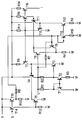
- an npn transistor T1 is provided, the emitter of which is connected to the reference potential M and the base and collector of which are connected to one another and are coupled via a common resistor R1 to an output terminal U carrying a reference potential.
- the base of an npn transistor T2 is connected to the base and collector of the transistor T1, the emitter of which is coupled to the reference potential M via a resistor R3 and the collector of which is coupled to the output terminal U via a resistor R2.
- the emitter of an npn transistor T4 is also connected to the output terminal U.
- the base of the transistor T4 is connected to the collector of an npn transistor T3, the emitter of which is connected to the reference potential M and the base of which is connected to the collector of the transistor T2.
- the base of the transistor T4 is also connected to the supply potential V via a current source circuit.
- the current source circuit has a pnp transistor T7, the emitter of which is connected via a resistor R5 to the supply potential V and the collector of which is connected to the base of transistor T4 or the collector of transistor T3 is connected.
- the base of the transistor T7 is connected to the base of a pnp transistor T8, the emitter of which is coupled to the supply potential V via a resistor R6.
- the collector of the transistor T8 is also connected to the collector of an npn transistor T6, the emitter of which is connected to the reference potential M via a resistor R4 and the base of which is connected to the output terminal U.
- an output connection I can also be provided which carries a reference current.
- the output terminal I is connected to the collector of a pnp transistor T16, the emitter of which is connected to the supply potential V via a resistor R14 and the base of which is connected to the bases of the transistors T7 and T8.
- the collector-emitter path of a pnp transistor T5 is connected in parallel.
- the emitter of transistor T5 is connected to the base of transistor T4 and the collector of transistor T5 is connected to reference potential M.
- Its base is controlled by a switching signal S with the interposition of a buffer stage.
- the buffer stage consists of a pnp transistor T14, at the base of which the switching signal S is applied, the emitter of which is coupled to the supply potential V and the collector of which is coupled to the base of the transistor T5 and, with the interposition of a resistor R12, to the reference potential M.
- a pnp transistor T5 an npn transistor could also be used in the same way with appropriate polarity and appropriate design of the switching signal S.
- the collector-emitter path of transistor T6 is the collector-emitter path of an npn transistor T9 connected in parallel.
- the base of the transistor T9 is driven by the switching signal S with the interposition of a resistor R8 and a further buffer stage. Accordingly, the emitters and the collectors of the transistors T6 and T9 are each connected to one another.
- the further buffer stage contains a pnp transistor T15, the emitter of which is connected to the supply potential V and the base of which is connected to the base of the transistor T14.
- the collector of the transistor T15 is coupled on the one hand to a connection of the resistor R8 and on the other hand via a resistor R13 to the reference potential M.
- the base of transistor T9 is also connected to the input branch of a current mirror.
- the input branch is formed by an npn transistor T13, the base and collector of which are connected to one another and to the base of the transistor T9 and whose emitter is connected to the reference potential M with the interposition of a resistor R10.
- the output branch of the current mirror is formed by an NPN transistor T12, the base of which is connected to the base of the transistor T13 and the emitter of which is connected to the reference potential M with the interposition of a resistor R9.
- the collector of the transistor T12 is based on a pnp transistor T10, the collector of which is connected to the reference potential M and the emitter of which is connected to the bases of the transistors T7 and T8, and of the emitter of an npn transistor T11, the collector of which is connected to the supply potential V and its base is connected to the collector of transistor T8. Finally, a resistor R11 is connected between the bases of the transistors T7 and T8 on the one hand and the supply potential V on the other.
- transistors T14 and T15 are blocked by the switching signal S, their collector potentials are approximately equal to the reference potential M.
- the transistor T5 is then also blocked and has no influence on the function of the other circuit parts. In this case, transistor T4 becomes its Function controlled accordingly.
- the transistor T15 supplies a starting current for the bandgap cell, which in the present exemplary embodiment consists of the transistors T1 and T2 and the resistors R1 to R3. If, on the other hand, the transistors T14 and T15 are turned on by the switching signal S, their respective collector potential is approximately equal to the supply potential V.
- the transistor T5 is also turned on and generates a potential at the base of the transistor T4 which also turns it off brings. The current consumption of the bandgap cell thus goes to zero.
- Resistor R8 and its combination with a complementary emitter follower consisting of transistors T10 and T11 support the switch-off process.
Landscapes
- Engineering & Computer Science (AREA)
- Microelectronics & Electronic Packaging (AREA)
- Physics & Mathematics (AREA)
- Power Engineering (AREA)
- Nonlinear Science (AREA)
- Electromagnetism (AREA)
- General Physics & Mathematics (AREA)
- Radar, Positioning & Navigation (AREA)
- Automation & Control Theory (AREA)
- Control Of Electrical Variables (AREA)
- Amplifiers (AREA)
Abstract
- mit einem zweiten Transistor (T2), dessen Basis mit der Basis des ersten Transistors (T1) verbunden ist,
- mit einem ersten Widerstand (R1), der zwischen den Kollektor des ersten Transistors (T1) und einen Ausgangsanschluß (U) zum Abgreifen des Referenzpotentials geschaltet ist,
- mit einem zweiten Widerstand (R2), der zwischen den Kollektor des zweiten Transistors (T2) und den Ausgangsanschluß (U) geschaltet ist,
- mit einem dritten Widerstand (R3), der zwischen Emitter des zweiten Transistors (T2) und das Bezugspotential (M) geschaltet ist,
- mit einem dritten Transistor (T3), dessen Basis mit dem Kollektor des zweiten Transistors (T2) und dessen Emitter mit dem Bezugspotential (M) verbunden ist, und
- mit einer gesteuerten Stromquelle (T4), die zwischen ein Versorgungspotential (V) und den Ausgangsanschluß (U) geschaltet ist und die eingangsseitig mit dem Kollektor des dritten Transistors (T3) gekoppelt ist, wobei der Kollektor-Emitter-Strecke des dritten Transistors (T3) die Kollektor-Emitter-Strecke eines fünften Transistors (T5) parallel geschaltet ist und daß die Basis des fünften Transistors (T5) durch ein Schaltsignal (S) angesteuert wird.
Description
- Die Erfindung betrifft eine ein-/ausschaltbare Schaltungsanordnung zur Erzeugung eines Referenzpotentials mit einem ersten Transistor, dessen Emitter mit einem Bezugspotential verbunden ist und dessen Basis und Kollektor miteinander verschaltet sind, mit einem zweiten Transistor, dessen Basis mit der Basis des ersten Transistors verbunden ist, mit einem ersten Widerstand, der zwischen den Kollektor des ersten Transistors und einem Ausgangsanschluß zum Abgreifen des Referenzpotentials geschaltet ist, mit einem zweiten Widerstand, der zwischen den Kollektor des zweiten Transistors und des Ausgangsanschluß geschaltet ist, mit einem dritten Widerstand, der zwischen den Emitter des zweiten Transistors und das Bezugspotential geschaltet ist, mit einem dritten Transistor, dessen Basis mit dem Kollektor des zweiten Transistors und dessen Emitter mit dem Bezugspotential verbunden ist, und mit einer gesteuerten Stromquelle, die zwischen ein Versorgungspotential und den Ausgangsanschluß geschaltet ist und die eingangsseitig mit dem Kollektor des dritten Transistors gekoppelt ist.
- Eine derartige, auch schaltbare Bandgap-Referenz bezeichnete Schaltungsanordnung ist beispielsweise aus Paul R. Gray, Robert G. Meyer, Analysis and Design of Analog Integrated Circuits, Second Edition, John Wiley and Sons, 1984, Seiten 293 bis 296, bekannt.
- In Zukunft wird es bei integrierten Schaltkreisen zunehmend wichtiger, daß zum Zwecke der Stromersparnis sich zumindest Teile der Schaltkreise Ein- und Ausschalten lassen. Demzufolge werden mehr und mehr auch ein- bzw. abschaltbare Referenzspannungsquellen verwendet, da die Referenzspannungsquelle im abgeschalteten Zustand möglichst keinen Strom verbrauchen sollte, bietet es sich an, die Referenzspannungsquelle durch eine in Serie geschaltete Schalteinrichtung ein-/abzuschalten. Üblicherweise liegt dabei ein pnp-Transistor in Reihe zu einer Bandgap-Referenz als Referenzspannungsquelle, so daß die Versorgungsspannung hoher sein muß, als eigentlich für die Bandgap-Referenz selbst notwendig ist. Außerdem lassen sich pnp-Transistoren in Standard-Technologie nur als großflächige Lateraltransistoren realisieren. Dabei ist häufig der Basisstrom zur Ansteuerung des pnp-Transistors nicht vernachlässigbar und erhöht die Stromaufnahme beim Betrieb.
- Aufgabe der Erfindung ist es, eine ein-/ausschaltbare Schaltungsanordnung zur Erzeugung eines Referenzpotentials anzugeben, die diese Nachteile nicht aufweist.
- Die Aufgabe wird durch eine Schaltungsanordnung gemäß Patentanspruch 1 gelöst. Ausgestaltungen und Weiterbildungen des Erfindungsgedankens sind Gegenstand von Unteransprüchen.
- Zur Vermeidung eines großen Flächenbedarfs und unnötiger Spannungs- und Stromverluste werden die Schaltmittel in die Bandgap-Referenz miteinbezogen. Insbesondere wird bei einer Schaltungsanordnung der eingangs genannten Art der Kollektor-Emitter-Strecke des dritten Transistors die Kollektor-Emitter-Strecke eines fünften Transistors parallel geschaltet und die Basis des fünften Transistors durch ein Schaltsignal angesteuert.
- Bei einer Ausgestaltung der Erfindung weist die gesteuerte Stromquelle einen vierten Transistor auf, dessen Kollektor mit dem Versorgungspotential, dessen Emitter mit dem Ausgangsanschluß und dessen Basis mit dem Kollektor des dritten Transistors verbunden ist. Zwischen Basis und Kollektor des vierten Transistors ist dabei eine weitere Stromquelle geschaltet. Weiterhin kann die weitere Stromquelle einen sechsten Transistor aufweisen, dessen Basis mit dem Ausgangsanschluß und dessen Emitter unter Zwischenschaltung eines vierten Widerstandes mit dem Bezugspotential verbunden ist. Des weiteren sind ein siebter Transistor, dessen Emitter unter Zwischenschaltung eines fünften Widerstandes mit dem Versorgungspotential verbunden ist, dessen Kollektor mit der Basis des vierten Transistors verschaltet ist und dessen Basis mit dem Kollektor des sechsten Transistors gekoppelt ist, sowie ein achter Transistor, dessen Basis und Kollektor miteinander sowie mit dem Kollektor des sechsten Transistors gekoppelt sind und dessen Emitter unter Zwischenschaltung eines sechsten Widerstandes mit dem Versorgungspotential verbunden ist, vorgesehen.
- Um die Anlaufeigenschaften beim Einschalten zu verbessern, wird vorgesehen, daß der Kollektor-Emitter-Strecke des sechsten Transistors die Kollektor-Emitter-Strecke eines neunten Transistors parallel geschaltet ist und daß dabei die Basis des neunten Transistors durch das Schaltsignal angesteuert wird.
- Darüber hinaus kann zwischen die Basen von sechstem und neuntem Transistor ein siebter Widerstand geschaltet werden. Ferner kann das Schaltsignal über einen achten Widerstand der Basis des neunten Transistors zugeführt werden.
- Eine Weiterbildung der Erfindung enthält einen zehnten Transistor, dessen Emitter mit den Basen von siebtem und achtem Transistor und dessen Kollektor mit dem Bezugspotential verbunden ist. Weiterhin ist ein elfter Transistor vorgesehen, dessen Kollektor mit dem Versorgungspotential, dessen Basis mit dem Kollektor des achten Transistors und dessen Emitter mit der Basis des zehnten Transistors verbunden ist. Die Basis des neunten Transistors ist dabei mit dem Eingangszweig eines Stromspiegels gekoppelt, dessen Ausgangszweig mit der Basis des zehnten Transistors gekoppelt ist.
- Zwischen die Basen von siebtem und achtem Transistor einerseits und das Versorgungspotential andererseits kann ein elfter Transistor geschaltet werden, der zur Erhöhung der Stabilität beiträgt.
- Schließlich kann vorgesehen werden, daß das Schaltsignal den Basen von fünftem und sechstem Transistor jeweils unter Zwischenschaltung einer Pufferstufe zugeführt wird.
- Die Erfindung wird nachfolgend anhand des in der einzigen Figur der Zeichnung dargestellten Ausführungsbeispiels näher erläutert.
- Bei der als Ausführungsbeispiel gezeigten erfindungsgemäßen Schaltungsanordnung ist ein npn-Transistor T1 vorgesehen, dessen Emitter mit dem Bezugspotential M verbunden ist und dessen Basis und Kollektor miteinander verschaltet und über einen gemeinsamen Widerstand R1 mit einem ein Referenzpotential führenden Ausgangsanschluß U gekoppelt sind. An Basis und Kollektor des Transistors T1 ist die Basis eines npn-Transistors T2 angeschlossen, dessen Emitter über einen Widerstand R3 mit dem Bezugspotential M und dessen Kollektor über einen Widerstand R2 mit dem Ausgangsanschluß U gekoppelt ist.
- An dem Ausgangsanschluß U ist darüber hinaus der Emitter eines npn-Transistors T4 angeschlossen, dessen Kollektor mit einem Versorgungspotential V verbunden ist. Die Basis des Transistors T4 ist mit dem Kollektor eines npn-Transistors T3 verbunden, dessen Emitter an das Bezugspotential M und dessen Basis an den Kollektor des Transistors T2 angeschlossen ist.
- Die Basis des Transistors T4 ist darüber hinaus über eine Stromquellenschaltung an das Versorgungspotential V angeschlossen. Die Stromquellenschaltung weist einen pnp-Transistor T7 auf, dessen Emitter über einen Widerstand R5 mit dem Versorgungspotential V und dessen Kollektor mit der Basis des Transistors T4 bzw. dem Kollektor des Transistors T3 verbunden ist. Die Basis des Transistors T7 ist mit der Basis eines pnp-Transistors T8 verschaltet, dessen Emitter über einen Widerstand R6 mit dem Versorgungspotential V gekoppelt ist. Der Kollektor des Transistors T8 ist darüber hinaus mit dem Kollektor eines npn-Transistors T6 verbunden, dessen Emitter über einen Widerstand R4 an das Bezugspotential M angeschlossen ist und dessen Basis mit dem Ausgangsanschluß U verbunden ist.
- Neben dem Ausgangsanschluß U, an dem das Referenzpotential abgreifbar ist, kann darüber hinaus ein Ausgangsanschluß I vorgesehen werden, der einen Referenzstrom führt. Dazu ist der Ausgangsanschluß I mit dem Kollektor eines pnp-Transistors T16 verbunden, dessen Emitter über einen Widerstand R14 mit dem Versorgungspotential V verbunden ist und dessen Basis mit den Basen der Transistoren T7 und T8 verschaltet ist.
- Erfindungsgemäß ist der Kollektor-Emitter-Strecke des Transistors T3 die Kollektor-Emitter-Strecke eines pnp-Transistors T5 parallel geschaltet. Somit ist der Emitter des Transistors T5 mit der Basis des Transistors T4 verbunden und der Kollektor des Transistors T5 an das Bezugspotential M angeschlossen. Seine Basis wird unter Zwischenschaltung einer Pufferstufe durch ein Schaltsignal S angesteuert. Die Pufferstufe besteht aus einem pnp-Transistor T14, an dessen Basis das Schaltsignal S angelegt ist, dessen Emitter mit dem Versorgungspotential V gekoppelt ist und dessen Kollektor mit der Basis des Transistors T5 sowie unter Zwischenschaltung eines Widerstandes R12 mit dem Bezugspotential M gekoppelt ist. Anstelle eines pnp-Transistors T5 könnte in gleicher Weise auch ein npn-Transistor bei entsprechender Polung sowie entsprechener Auslegung des Schaltsignals S verwendet werden.
- Weiterhin ist der Kollektor-Emitter-Strecke des Transistors T6 die Kollektor-Emitter-Strecke eines npn-Transistors T9 parallel geschaltet. Die Basis des Transistors T9 wird unter Zwischenschaltung eines Widerstandes R8 sowie einer weiteren Pufferstufe durch das Schaltsignal S angesteuert. Demgemäß sind die Emitter und die Kollektoren der Transistoren T6 und T9 jeweils miteinander verschaltet. Die weitere Pufferstufe enthält einen pnp-Transistor T15, dessen Emitter mit dem Versorgungspotential V und dessen Basis mit der Basis des Transistors T14 verbunden ist. Der Kollektor des Transistors T15 ist zum einen mit einem Anschluß des Widerstandes R8 und zum anderen über einen Widerstand R13 mit dem Bezugspotential M gekoppelt.
- Die Basis des Transistors T9 ist zudem mit dem Eingangszweig eines Stromspiegels verbunden. Der Eingangszweig wird durch einen npn-Transistor T13 gebildet, dessen Basis und Kollektor miteinander sowie mit der Basis des Transistors T9 verschaltet sind und dessen Emitter unter Zwischenschaltung eines Widerstandes R10 an das Bezugspotential M angeschlossen ist. Der Ausgangszweig des Stromspiegels wird durch einen npn-Transistor T12 gebildet, dessen Basis mit der Basis des Transistors T13 verbunden ist und dessen Emitter unter Zwischenschaltung eines Widerstandes R9 an das Bezugspotential M angeschlossen ist. Der Kollektor des Transistors T12 ist auf die Basis eines pnp-Transistors T10, dessen Kollektor mit dem Bezugspotential M und dessen Emitter mit den Basen der Transistoren T7 und T8 verbunden ist, sowie auf den Emitter eines npn-Transistors T11, dessen Kollektor mit dem Versorgungspotential V und dessen Basis mit dem Kollektor des Transistors T8 verschaltet ist, geführt. Schließlich ist ein Widerstand R11 zwischen die Basen der Transistoren T7 und T8 einerseits und das Versorgungspotential V andererseits geschaltet.
- Werden die Transistoren T14 und T15 durch das Schaltsignal S gesperrt, so sind ihre Kollektorpotentiale annähernd gleich dem Bezugspotential M. Der Transistor T5 ist dann ebenfalls gesperrt und hat auf die Funktion der übrigen Schaltungsteile keinen Einfluß. Der Transistor T4 wird in diesem Fall seiner Funktion entsprechend angesteuert. Der Transistor T15 liefert einen Anlaufstrom für die Bandgap-Zelle, die beim vorliegenden Ausführungsbeispiel aus den Transistoren T1 und T2 sowie den Widerständen R1 bis R3 besteht. Werden dagegen die Transistoren T14 und T15 durch das Schaltsignal S durchgesteuert, so ist ihr jeweiliges Kollektorpotential in etwa gleich dem Versorgungspotential V. Der Transistor T5 ist dabei ebenfalls durchgesteuert und erzeugt an der Basis des Transistors T4 ein Potential, das diesen ebenfalls in den sperrenden Zustand bringt. Die Stromaufnahme der Bandgap-Zelle geht damit gegen Null. Der Widerstand R8 sowie dessen Kombination mit einem aus den Transistoren T10 und T11 bestehenden komplementären Emitterfolger unterstützen den Abschaltvorgang.
- Damit liegt in Reihe zur Bandgap-Zelle nur der ohnehin notwendige Transistor T4. Ein weiterer Ein/Ausschalttran-sistor ist nicht notwendig. Somit wird ein serieller Spannungsabfall vermieden und darüber hinaus der zusätzliche Flächenbedarf gering gehalten. Mittels der Transistoren T9 bis T13 in Verbindung mit den Widerständen R8 und R11 werden auch die übrigen Schaltungsteile weitgehend stromlos gehalten, so daß insgesamt der Stromverbrauch im Ruhezustand sowie der gegenüber dem Versorgungsstrom im Betriebsfall notwendige Strom für die Abschalteinrichtungen äußerst gering ist.
Claims (9)
- Ein-/Ausschaltbare Schaltungsanordnung zur Erzeugung eines Referenzpotentials mit einem ersten Transistor (T1), dessen Emitter mit einem Bezugspotential (M) verbunden ist und dessen Basis und Kollektor miteinander verschaltet sind,mit einem zweiten Transistor (T2), dessen Basis mit der Basis des ersten Transistors (T1) verbunden ist,mit einem ersten Widerstand (R1), der zwischen den Kollektor des ersten Transistors (T1) und einen Ausgangsanschluß (U) zum Abgreifen des Referenzpotentials geschaltet ist,mit einem zweiten Widerstand (R2), der zwischen den Kollektor des zweiten Transistors (T2) und den Ausgangsanschluß (U) geschaltet ist,mit einem dritten Widerstand (R3), der zwischen Emitter des zweiten Transistors (T2) und das Bezugspotential (M) geschaltet ist,mit einem dritten Transistor (T3), dessen Basis mit dem Kollektor des zweiten Transistors (T2) und dessen Emitter mit dem Bezugspotential (M) verbunden ist, undmit einer gesteuerten Stromquelle (T4), die zwischen ein Versorgungspotential (V) und den Ausgangsanschluß (U) geschaltet ist und die eingangsseitig mit dem Kollektor des dritten Transistors (T3) gekoppelt ist,
dadurch gekennzeichnet, daß der Kollektor-Emitter-Strecke des dritten Transistors (T3) die Kollektor-Emitter-Strecke eines fünften Transistors (T5) parallel geschaltet ist und daß die Basis des fünften Transistors (T5) durch ein Schaltsignal (S) angesteuert wird. - Schaltungsanordnung nach Anspruch 1,
dadurch gekennzeichnet, daß die gesteuerte Stromquelle (T4) einen vierten Transistor (T4) aufweist, dessen Kollektor mit dem Versorgungspotential (V), dessen Emitter mit dem Ausgangsanschluß (U) und dessen Basis mit dem Kollektor des dritten Transistors (T3) verbunden ist, und daß zwischen Basis und Kollektor des vierten Transistors (T4) eine weitere Stromquelle (T7, T8, R4, R5, R6) geschaltet ist. - Schaltungsanordnung nach Anspruch 2,
dadurch gekennzeichnet, daß die weitere Stromquelle (T6, T7, T8, R4, R5, R6) aufweist:einen sechsten Transistor (T6), dessen Basis mit dem Ausgangsanschluß (U) und dessen Emitter unter Zwischenschaltung eines vierten Widerstandes mit dem Bezugspotential (M) verbunden ist;einen siebten Transistor (T7), dessen Emitter unter Zwischenschaltung eines fünften Widerstandes (R5) mit dem Versorgungspotential (V) verbunden ist, dessen Kollektor mit der Basis des fünften Transistors (T5) verschaltet ist und dessen Basis mit dem Kollektor des sechsten Transistors (T6) gekoppelt ist;einen achten Transistor (T8), dessen Basis und Kollektor miteinander sowie mit dem Kollektor des sechsten Transistors (T6) gekoppelt sind und dessen Emitter unter Zwischenschaltung eines sechsten Widerstandes (R6) mit dem Versorgungspotential (V) verbunden ist. - Schaltungsanordnung nach Anspruch 2 oder 3,
dadurch gekennzeichnet, daß der Kollektor-Emitter-Strecke des sechsten Transistors (T6) die Kollektor-Emitter-Strecke eines neunten Transistors (T9) parallel geschaltet ist und daß die Basis des neunten Transistors (T9) durch das Schaltsignal (S) angesteuert wird. - Schaltungsanordnung nach Anspruch 4,
dadurch gekennzeichnet, daß zwischen die Basis von sechstem und neuntem Transistor (T6, T9) ein siebter Widerstand (R7) geschaltet ist. - Schaltungsanordnung nach Anspruch 4 oder 5,
dadurch gekennzeichnet, daß das Schaltsignal (S) über einen achten Widerstand (R8) der Basis des neunten Transistors (T9) zugeführt wird. - Schaltungsanordnung nach einem der Ansprüche 4 bis 6,
gekennzeichnet durch einen zehnten Transistor (T10), dessen Emitter mit den Basen von siebtem und achtem Transistor (T7, T8) und dessen Kollektor mit dem Bezugspotential verbunden ist, durch einen elften Transistor (T11), dessen Kollektor mit dem Versorgungspotential (V), dessen Basis mit dem Kollektor des achten Transistors (T8) und dessen Emitter mit der Basis des zehnten Transistors (T10) verbunden ist, und durch einen Stromspiegel (T12, T13, R9, R10), dessen Eingangszweig mit der Basis des neunten Transistors (T9) und dessen Ausgangszweig mit der Basis des zehnten Transistors (T10) gekoppelt ist. - Schaltungsanordnung nach einem der Ansprüche 3 bis 7,
dadurch gekennzeichnet, daß zwischen die Basen von siebtem und achtem Transistor (T7, T8) einerseits und das Versorgungspotential (V) andererseits ein elfter Widerstand (R11) geschaltet ist. - Schaltungsanordnung nach einem der Ansprüche 4 bis 8,
dadurch gekennzeichnet, daß das Schaltsignal (S) den Basen von fünftem und neuntem Transistor (T5, T9) jeweils unter Zwischenschaltung einer Pufferstufe (T14, R12; T15, R13) zugeführt wird.
Applications Claiming Priority (2)
| Application Number | Priority Date | Filing Date | Title |
|---|---|---|---|
| DE19621110 | 1996-05-24 | ||
| DE19621110A DE19621110C1 (de) | 1996-05-24 | 1996-05-24 | Ein-/Ausschaltbare Schaltungsanordnung zur Erzeugung eines Referenzpotentials |
Publications (3)
| Publication Number | Publication Date |
|---|---|
| EP0809169A2 true EP0809169A2 (de) | 1997-11-26 |
| EP0809169A3 EP0809169A3 (de) | 1998-12-09 |
| EP0809169B1 EP0809169B1 (de) | 2000-08-09 |
Family
ID=7795317
Family Applications (1)
| Application Number | Title | Priority Date | Filing Date |
|---|---|---|---|
| EP97107599A Expired - Lifetime EP0809169B1 (de) | 1996-05-24 | 1997-05-05 | Ein-/Ausschaltbare Schaltungsanordnung zur Erzeugung eines Referenzpotentials |
Country Status (4)
| Country | Link |
|---|---|
| US (1) | US5801582A (de) |
| EP (1) | EP0809169B1 (de) |
| DE (2) | DE19621110C1 (de) |
| IN (1) | IN191847B (de) |
Families Citing this family (5)
| Publication number | Priority date | Publication date | Assignee | Title |
|---|---|---|---|---|
| DE19624676C1 (de) * | 1996-06-20 | 1997-10-02 | Siemens Ag | Schaltungsanordnung zur Erzeugung eines Referenzpotentials |
| JP4116133B2 (ja) * | 1997-07-31 | 2008-07-09 | 株式会社東芝 | 温度依存型定電流発生回路およびこれを用いた光半導体素子の駆動回路 |
| US6097179A (en) * | 1999-03-08 | 2000-08-01 | Texas Instruments Incorporated | Temperature compensating compact voltage regulator for integrated circuit device |
| JP4212036B2 (ja) * | 2003-06-19 | 2009-01-21 | ローム株式会社 | 定電圧発生器 |
| EP1501001A1 (de) * | 2003-07-22 | 2005-01-26 | STMicroelectronics Limited | Vorspannungsschaltung |
Family Cites Families (9)
| Publication number | Priority date | Publication date | Assignee | Title |
|---|---|---|---|---|
| JPH0727425B2 (ja) * | 1988-12-28 | 1995-03-29 | 株式会社東芝 | 電圧発生回路 |
| US5013934A (en) * | 1989-05-08 | 1991-05-07 | National Semiconductor Corporation | Bandgap threshold circuit with hysteresis |
| JPH0680486B2 (ja) * | 1989-08-03 | 1994-10-12 | 株式会社東芝 | 定電圧回路 |
| US5278491A (en) * | 1989-08-03 | 1994-01-11 | Kabushiki Kaisha Toshiba | Constant voltage circuit |
| JP3322685B2 (ja) * | 1992-03-02 | 2002-09-09 | 日本テキサス・インスツルメンツ株式会社 | 定電圧回路および定電流回路 |
| JP3381937B2 (ja) * | 1992-05-22 | 2003-03-04 | 株式会社東芝 | 中間電位発生回路 |
| JP3318365B2 (ja) * | 1992-10-20 | 2002-08-26 | 富士通株式会社 | 定電圧回路 |
| FR2711258A1 (fr) * | 1993-10-13 | 1995-04-21 | Philips Composants | Circuit générateur de tension stabilisée du type bandgap. |
| US5703476A (en) * | 1995-06-30 | 1997-12-30 | Sgs-Thomson Microelectronics, S.R.L. | Reference voltage generator, having a double slope temperature characteristic, for a voltage regulator of an automotive alternator |
-
1996
- 1996-05-24 DE DE19621110A patent/DE19621110C1/de not_active Expired - Fee Related
-
1997
- 1997-05-05 EP EP97107599A patent/EP0809169B1/de not_active Expired - Lifetime
- 1997-05-05 DE DE59702125T patent/DE59702125D1/de not_active Expired - Lifetime
- 1997-05-23 US US08/862,239 patent/US5801582A/en not_active Expired - Lifetime
- 1997-05-26 IN IN951CA1997 patent/IN191847B/en unknown
Also Published As
| Publication number | Publication date |
|---|---|
| EP0809169A3 (de) | 1998-12-09 |
| US5801582A (en) | 1998-09-01 |
| DE59702125D1 (de) | 2000-09-14 |
| EP0809169B1 (de) | 2000-08-09 |
| IN191847B (de) | 2004-01-10 |
| DE19621110C1 (de) | 1997-06-12 |
Similar Documents
| Publication | Publication Date | Title |
|---|---|---|
| DE68924394T2 (de) | Vorrichtung zum Erzeugen einer Referenzspannung für einen eine kapazitive Bootstrapschaltung enthaltenden Schalter. | |
| DE4221430B4 (de) | Bezugsspannungsschaltung mit schnellem Hochfahren der Leistung ausgehend von einem Bereitschaftszustand mit niedriger Leistung | |
| DE69019784T2 (de) | Geschaltete Brückenanordnung. | |
| EP0595069A1 (de) | Schaltstufe in Stromschaltertechnik | |
| DE2210105C3 (de) | Verknüpfungsschaltung | |
| EP0814396B1 (de) | Schaltungsanordnung zur Erzeugung eines Referenzpotentials | |
| EP0809169B1 (de) | Ein-/Ausschaltbare Schaltungsanordnung zur Erzeugung eines Referenzpotentials | |
| EP0583688B1 (de) | Digitaler Stromschalter | |
| EP0011704B1 (de) | Referenzspannungsquelle, insbesondere für Verstärkerschaltungen | |
| EP0421016A1 (de) | ECL-TTL-Signalpegelwandler | |
| DE69031019T2 (de) | Ausgangssteuerungsschaltung | |
| EP0196627B1 (de) | Integrierte Verstärkerschaltung | |
| DE68919494T2 (de) | Operationsverstärker. | |
| EP0673118A1 (de) | BiCMOS-Pegelwandler ECL-CMOS | |
| EP0442001B1 (de) | Komparatorschaltung | |
| EP0682305B1 (de) | Schaltungsanordnung zur Erzeugung eines Referenzstroms | |
| EP0578098B1 (de) | Integrierbare Treiberschaltung für eine reaktive Last | |
| DE3509595A1 (de) | Schaltungsanordnung | |
| DE3036736A1 (de) | Schaltungsanordnung zur belastungsproportionalen einstellung des ansteuerstroms eines in emitterschaltung betriebenen eintakt-endstufentransistors eines transistorverstaerkers | |
| DE1246027B (de) | Logische Schaltung aus zwei in Stromuebernahme-schaltung geschalteten Transistoren | |
| DE9211278U1 (de) | Schaltungsanordnung zum Stummschalten von Tonteilen | |
| EP0806719A2 (de) | Schaltungsanordnung zur Erzeugung eines Referenz-potentials | |
| EP0792021A1 (de) | Treiberschaltung | |
| EP0495141B1 (de) | Amplitudenregeleinrichtung | |
| DE19928796B4 (de) | Elektronischer Schalter zum Schalten einer Last |
Legal Events
| Date | Code | Title | Description |
|---|---|---|---|
| PUAI | Public reference made under article 153(3) epc to a published international application that has entered the european phase |
Free format text: ORIGINAL CODE: 0009012 |
|
| AK | Designated contracting states |
Kind code of ref document: A2 Designated state(s): DE FR GB IT |
|
| PUAL | Search report despatched |
Free format text: ORIGINAL CODE: 0009013 |
|
| AK | Designated contracting states |
Kind code of ref document: A3 Designated state(s): DE FR GB IT |
|
| 17P | Request for examination filed |
Effective date: 19990105 |
|
| GRAG | Despatch of communication of intention to grant |
Free format text: ORIGINAL CODE: EPIDOS AGRA |
|
| GRAG | Despatch of communication of intention to grant |
Free format text: ORIGINAL CODE: EPIDOS AGRA |
|
| GRAH | Despatch of communication of intention to grant a patent |
Free format text: ORIGINAL CODE: EPIDOS IGRA |
|
| 17Q | First examination report despatched |
Effective date: 19991021 |
|
| GRAH | Despatch of communication of intention to grant a patent |
Free format text: ORIGINAL CODE: EPIDOS IGRA |
|
| GRAA | (expected) grant |
Free format text: ORIGINAL CODE: 0009210 |
|
| AK | Designated contracting states |
Kind code of ref document: B1 Designated state(s): DE FR GB IT |
|
| REF | Corresponds to: |
Ref document number: 59702125 Country of ref document: DE Date of ref document: 20000914 |
|
| ITF | It: translation for a ep patent filed | ||
| GBT | Gb: translation of ep patent filed (gb section 77(6)(a)/1977) |
Effective date: 20001010 |
|
| ET | Fr: translation filed | ||
| PLBE | No opposition filed within time limit |
Free format text: ORIGINAL CODE: 0009261 |
|
| STAA | Information on the status of an ep patent application or granted ep patent |
Free format text: STATUS: NO OPPOSITION FILED WITHIN TIME LIMIT |
|
| 26N | No opposition filed | ||
| REG | Reference to a national code |
Ref country code: GB Ref legal event code: IF02 |
|
| PGFP | Annual fee paid to national office [announced via postgrant information from national office to epo] |
Ref country code: FR Payment date: 20030512 Year of fee payment: 7 |
|
| PGFP | Annual fee paid to national office [announced via postgrant information from national office to epo] |
Ref country code: GB Payment date: 20040427 Year of fee payment: 8 |
|
| PG25 | Lapsed in a contracting state [announced via postgrant information from national office to epo] |
Ref country code: FR Free format text: LAPSE BECAUSE OF NON-PAYMENT OF DUE FEES Effective date: 20050131 |
|
| REG | Reference to a national code |
Ref country code: FR Ref legal event code: ST |
|
| PG25 | Lapsed in a contracting state [announced via postgrant information from national office to epo] |
Ref country code: IT Free format text: LAPSE BECAUSE OF NON-PAYMENT OF DUE FEES Effective date: 20050505 Ref country code: GB Free format text: LAPSE BECAUSE OF NON-PAYMENT OF DUE FEES Effective date: 20050505 |
|
| GBPC | Gb: european patent ceased through non-payment of renewal fee |
Effective date: 20050505 |
|
| REG | Reference to a national code |
Ref country code: DE Ref legal event code: R081 Ref document number: 59702125 Country of ref document: DE Owner name: INTEL MOBILE COMMUNICATIONS GMBH, DE Free format text: FORMER OWNER: SIEMENS AKTIENGESELLSCHAFT, 80333 MUENCHEN, DE Effective date: 20111107 Ref country code: DE Ref legal event code: R081 Ref document number: 59702125 Country of ref document: DE Owner name: INTEL MOBILE COMMUNICATIONS TECHNOLOGY GMBH, DE Free format text: FORMER OWNER: SIEMENS AKTIENGESELLSCHAFT, 80333 MUENCHEN, DE Effective date: 20111107 |
|
| REG | Reference to a national code |
Ref country code: DE Ref legal event code: R081 Ref document number: 59702125 Country of ref document: DE Owner name: INTEL MOBILE COMMUNICATIONS GMBH, DE Free format text: FORMER OWNER: INTEL MOBILE COMMUNICATIONS TECHNOLOGY GMBH, 85579 NEUBIBERG, DE Effective date: 20130326 Ref country code: DE Ref legal event code: R081 Ref document number: 59702125 Country of ref document: DE Owner name: INTEL MOBILE COMMUNICATIONS GMBH, DE Free format text: FORMER OWNER: INFINEON TECHNOLOGIES AG, 85579 NEUBIBERG, DE Effective date: 20130314 Ref country code: DE Ref legal event code: R081 Ref document number: 59702125 Country of ref document: DE Owner name: INTEL MOBILE COMMUNICATIONS GMBH, DE Free format text: FORMER OWNER: INFINEON TECHNOLOGIES AG, 85579 NEUBIBERG, DE Effective date: 20130315 Ref country code: DE Ref legal event code: R081 Ref document number: 59702125 Country of ref document: DE Owner name: INTEL MOBILE COMMUNICATIONS GMBH, DE Free format text: FORMER OWNER: INTEL MOBILE COMMUNICATIONS GMBH, 85579 NEUBIBERG, DE Effective date: 20130315 |
|
| PGFP | Annual fee paid to national office [announced via postgrant information from national office to epo] |
Ref country code: DE Payment date: 20140430 Year of fee payment: 18 |
|
| REG | Reference to a national code |
Ref country code: DE Ref legal event code: R119 Ref document number: 59702125 Country of ref document: DE |
|
| PG25 | Lapsed in a contracting state [announced via postgrant information from national office to epo] |
Ref country code: DE Free format text: LAPSE BECAUSE OF NON-PAYMENT OF DUE FEES Effective date: 20151201 |