EP0807973B1 - Dispositif semi-conducteur du type à incapsulation en plastique et procédé de fabrication - Google Patents
Dispositif semi-conducteur du type à incapsulation en plastique et procédé de fabrication Download PDFInfo
- Publication number
- EP0807973B1 EP0807973B1 EP97302914A EP97302914A EP0807973B1 EP 0807973 B1 EP0807973 B1 EP 0807973B1 EP 97302914 A EP97302914 A EP 97302914A EP 97302914 A EP97302914 A EP 97302914A EP 0807973 B1 EP0807973 B1 EP 0807973B1
- Authority
- EP
- European Patent Office
- Prior art keywords
- dambar
- leads
- dambars
- semiconductor device
- lead frame
- Prior art date
- Legal status (The legal status is an assumption and is not a legal conclusion. Google has not performed a legal analysis and makes no representation as to the accuracy of the status listed.)
- Expired - Lifetime
Links
Images


Classifications
-
- H—ELECTRICITY
- H10—SEMICONDUCTOR DEVICES; ELECTRIC SOLID-STATE DEVICES NOT OTHERWISE PROVIDED FOR
- H10W—GENERIC PACKAGES, INTERCONNECTIONS, CONNECTORS OR OTHER CONSTRUCTIONAL DETAILS OF DEVICES COVERED BY CLASS H10
- H10W74/00—Encapsulations, e.g. protective coatings
- H10W74/01—Manufacture or treatment
- H10W74/016—Manufacture or treatment using moulds
-
- H—ELECTRICITY
- H10—SEMICONDUCTOR DEVICES; ELECTRIC SOLID-STATE DEVICES NOT OTHERWISE PROVIDED FOR
- H10W—GENERIC PACKAGES, INTERCONNECTIONS, CONNECTORS OR OTHER CONSTRUCTIONAL DETAILS OF DEVICES COVERED BY CLASS H10
- H10W70/00—Package substrates; Interposers; Redistribution layers [RDL]
- H10W70/40—Leadframes
- H10W70/411—Chip-supporting parts, e.g. die pads
- H10W70/415—Leadframe inner leads serving as die pads
-
- H—ELECTRICITY
- H10—SEMICONDUCTOR DEVICES; ELECTRIC SOLID-STATE DEVICES NOT OTHERWISE PROVIDED FOR
- H10W—GENERIC PACKAGES, INTERCONNECTIONS, CONNECTORS OR OTHER CONSTRUCTIONAL DETAILS OF DEVICES COVERED BY CLASS H10
- H10W74/00—Encapsulations, e.g. protective coatings
- H10W74/10—Encapsulations, e.g. protective coatings characterised by their shape or disposition
- H10W74/111—Encapsulations, e.g. protective coatings characterised by their shape or disposition the semiconductor body being completely enclosed
- H10W74/129—Encapsulations, e.g. protective coatings characterised by their shape or disposition the semiconductor body being completely enclosed forming a chip-scale package [CSP]
-
- H—ELECTRICITY
- H10—SEMICONDUCTOR DEVICES; ELECTRIC SOLID-STATE DEVICES NOT OTHERWISE PROVIDED FOR
- H10W—GENERIC PACKAGES, INTERCONNECTIONS, CONNECTORS OR OTHER CONSTRUCTIONAL DETAILS OF DEVICES COVERED BY CLASS H10
- H10W72/00—Interconnections or connectors in packages
- H10W72/50—Bond wires
- H10W72/531—Shapes of wire connectors
- H10W72/536—Shapes of wire connectors the connected ends being ball-shaped
-
- H—ELECTRICITY
- H10—SEMICONDUCTOR DEVICES; ELECTRIC SOLID-STATE DEVICES NOT OTHERWISE PROVIDED FOR
- H10W—GENERIC PACKAGES, INTERCONNECTIONS, CONNECTORS OR OTHER CONSTRUCTIONAL DETAILS OF DEVICES COVERED BY CLASS H10
- H10W72/00—Interconnections or connectors in packages
- H10W72/50—Bond wires
- H10W72/531—Shapes of wire connectors
- H10W72/5363—Shapes of wire connectors the connected ends being wedge-shaped
-
- H—ELECTRICITY
- H10—SEMICONDUCTOR DEVICES; ELECTRIC SOLID-STATE DEVICES NOT OTHERWISE PROVIDED FOR
- H10W—GENERIC PACKAGES, INTERCONNECTIONS, CONNECTORS OR OTHER CONSTRUCTIONAL DETAILS OF DEVICES COVERED BY CLASS H10
- H10W72/00—Interconnections or connectors in packages
- H10W72/50—Bond wires
- H10W72/551—Materials of bond wires
- H10W72/552—Materials of bond wires comprising metals or metalloids, e.g. silver
- H10W72/5522—Materials of bond wires comprising metals or metalloids, e.g. silver comprising gold [Au]
-
- H—ELECTRICITY
- H10—SEMICONDUCTOR DEVICES; ELECTRIC SOLID-STATE DEVICES NOT OTHERWISE PROVIDED FOR
- H10W—GENERIC PACKAGES, INTERCONNECTIONS, CONNECTORS OR OTHER CONSTRUCTIONAL DETAILS OF DEVICES COVERED BY CLASS H10
- H10W90/00—Package configurations
- H10W90/701—Package configurations characterised by the relative positions of pads or connectors relative to package parts
- H10W90/751—Package configurations characterised by the relative positions of pads or connectors relative to package parts of bond wires
- H10W90/756—Package configurations characterised by the relative positions of pads or connectors relative to package parts of bond wires between a chip and a stacked lead frame, conducting package substrate or heat sink
Definitions
- This invention relates to a resin- or plastic-molded type semiconductor device and a method of manufacturing it.
- FIG. 23(a) and 23(b) One example of structures of the semiconductor devices is shown in Figs. 23(a) and 23(b) .
- reference numeral 1 indicates a plastic molded type semiconductor device and reference numeral 2 indicates a semiconductor element.
- the semiconductor element 2 has one surface to which a chip support 4 is bonded and fixed by an insulating adhesive tape 3. Further, leads 6 are electrically connected to the semiconductor element 2 through gold wires 5 connected to both sides of the chip support 4.
- the plastic molded type semiconductor device 1 is formed by sealing the semiconductor element 2 with a mold resin 7 so that the upper surface of the chip support 4 and the bottom face of the semiconductor element 2 are exposed.
- the semiconductor device can be made thin correspondingly.
- US Patent 5,444,301 discloses a resin - or plastic molded type semiconductor device.
- the resin- or plastic-molded type semiconductor device of the present invention comprises a semiconductor element having electrodes provided on a surface thereof, a plurality of leads respectively electrically connected to the electrodes, a sealing material formed so as to expose parts of the leads and a dambar formed along the outer periphery of the surface of the semiconductor element, wherein the electrodes are provided inside the dambar electrically independent of the dambar and the sealing material is formed within a region surrounded by the dambar.
- the invention also provides a method of manufacturing a resin- or plastic-molded type semiconductor device comprising the following steps: a step for preparing semiconductor elements each having electrodes provided on a surface thereof; a step for forming a lead frame having frame-shaped dambars having an outer shape substantially identical to that of the surface of respective ones of said semiconductor elements and a plurality of leads disposed within said each of dambars and electrically independent thereof, each of said dambars and its respective leads being fixed to each other with an insulating adhesive tape; a step for placing said lead frame on the surface of said each of said semiconductor elements so that each of said dambars substantially coincide in outer edge with the surface of said respective semiconductor element and fixing said leads and said dambar onto said respective semiconductor element with the adhesive tape; a step for electrically connecting said leads and said respective semiconductor elements to each other with conductive wires; and a step for filling the inside of each of said dambars with a sealing material within a mold so as to seal the surfaces of said semiconductor elements and to expose parts of said respective leads.
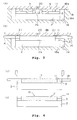
- FIGs. 1(a) and 1(b) respectively show a first embodiment of the present invention.
- the same elements of structure as those shown in Figs. 23(a) and 23(b) are identified by the same reference numerals (the drawings illustrative of a second embodiment and embodiments subsequent thereto, which will be described below, are also similar to the above).
- reference numeral 10 indicates a resin or plastic molded type semiconductor device (hereinafter abbreviated as "semiconductor device").
- the semiconductor device 10 comprises a rectangular and plate-shaped semiconductor element 2, a plurality of leads 6 electrically connected to a circuit forming surface 2a of the semiconductor element 2, a plurality of gold lines or wires 5 for respectively electrically connecting the semiconductor element 2 and the leads 6 to each other on the circuit forming surface 2a, and an insulating adhesive tape 3 provided between the leads 6 and the semiconductor element 2 so as to fix the leads 6 to the semiconductor element 2.
- the leads 6 are disposed over the circuit forming surface 2a of the semiconductor element 2 and provided not so as to extend toward the sides of the circuit forming surface 2a. Further, the leads 6 are respectively subjected to downset processing so as to be formed with differences in level by the thickness of the adhesive tape 3. A lower portion 6a of each lead 6 is brought into contact with the semiconductor element 2, whereas an upper portion 6b thereof is bonded and fixed onto the semiconductor element 2 with the adhesive tape 3 interposed therebetween. As shown in Fig. 1(b) , these leads 6 are provided over the semiconductor element 2 in two rows.
- the gold wires 5 for respectively electrically connecting the leads 6 and the semiconductor element 2 to one another are electrically connected to their corresponding upper surfaces of the lower portions 6a of the leads 6 and are disposed not so as to extend out upwardly from the upper surfaces of the upper portions 6b of the leads 6.
- the adhesive tape 3 is composed of, for example, a polyimide resin and has unillustrated adhesive layers formed on both surfaces thereof. Further, the adhesive tape 3 is shaped in the form of a rectangular frame and bonded onto the circuit forming surface 2a in a state in which its outer peripheral edge has substantially matched with its corresponding outer shape of the circuit forming surface 2a.
- a dambar 11 is fixed onto the circuit forming surface 2a of the semiconductor element 2 by the adhesive tape 3.
- the dambar 11 has an outer shape substantially identical to the outer shape of the circuit forming surface 2a and is formed in the same thickness as that of each lead 6.
- the dambar 11 is provided not so as to make contact with the leads 6 and disposed so that its outer edge substantially coincides with the outer edge of the circuit forming surface 2a.
- a mold resin 7 is charged and hardened inside the dambar 11 on the circuit forming surface 2a of the semiconductor element 2.
- the circuit forming surface 2a is sealed by the mold resin 7 in a state in which the upper surface of the dambar 11 and the upper surfaces of the upper portions 6a of the leads 6 have been exposed.
- the semiconductor element 2 thereof has surfaces other than the circuit forming surface 2a, which have been exposed under the aforementioned resin sealing of the circuit forming surface 2a by the mold resin.
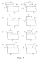
- a lead frame 12 shown in Fig. 2(a) is first prepared.
- the lead frame 12 comprises a metal lead frame member 13 shaped in the form of a rectangular frame, and a plurality of lead frame bodies 15 connected to the inside of the lead frame member 13 through metal dambar supports 14.
- the lead frame bodies 15 are respectively formed of metal dambars 11 shaped in the form of rectangular frames, which are connected to one another through the dambar supports 14, a plurality of metal leads 6 disposed within each dambar 11 without contacting the dambar 11, and an adhesive tape 3 for coupling these leads 6 to the dambars 11.
- each lead frame body 15 As the lead frame body, one is first prepared as shown in Fig. 2(d) , which comprises a dambar 11, a lead support 16 connected to the dambar 11, and leads 6 respectively coupled to both sides of the lead support 16. Next, the connecting sides of the leads 6, i.e., the ends thereof on the lead support 16 side are given metal plating 17 as shown in Fig. 2(e) . Further, the adhesive tape 3 is placed on the surfaces of the leads 6, which are opposite to the surfaces thereof provided with the metal plating 17.
- the adhesive tape 3 is a frame-shaped one having an outer shape substantially identical to that of the dambar 11.
- the adhesive tape 3 one is used which covers the entire back (corresponding to the same surface as the surface on the side opposite to each metal plating 17 applied to each lead 6) of the dambar 11 and has shapes and dimensions required to couple the dambar 11 and the leads 6 to one another. In regard to the portions stuck on the leads 6, however, the size of the adhesive tape 3 is adjusted so that the adhesive tape 3 is bonded only onto the back of each lead 6 on the side uncoated with the metal plating 17.
- the downset processing is applied to the side of each lead 6 to which no adhesive tape 3 is bonded. Further, the lead support 16 is separated from the dambar 11 and the leads 6 to obtain the lead frame body 15 shown in Figs. 2(b) and 2(c) .
- the lead frame 12 which has been prepared in this way, is placed on the semiconductor element 2 in such a manner that the outer edge of the dambar 11 of the lead frame body 15 substantially coincides with the outer edge of the circuit forming surface of the semiconductor element 2. Further, the leads 6 and the dambar 11 are fixed onto the semiconductor element 2 with the adhesive tape 3 by thermo compression bonding.
- Fig. 3(a) shows the side of the semiconductor device 10 as seen in the direction indicated by arrow A in Fig. 1(b) .
- Fig. 3(b) illustrates the side of the semiconductor device 10 as seen in the direction indicated by arrow B in Fig. 1(b) .
- the mold 18 As the mold 18, one is used in which the depth of the cavity 19 defined in a cavity-retainer plate or lower form 18a is equal to the total thickness of the semiconductor element 2, adhesive tape 3 and dambar 11. Thus, the mold 18 is held within the cavity 19 in a state in which the bottom face (corresponding to the surface opposite to the circuit forming surface) of the semiconductor element 2 and the upper surfaces of the dambar 11 and each lead 6 are interposed between the bottom face and top face (corresponding to the lower surface of an upper form 18b) that form the cavity 19. Further, the mold 18 has a resin injection hole 20 and degassing holes 21 (see Fig. 3(b) ) defined in the upper form 18b thereof. Each of dambar supports 14 of the lead frame 12 is interposed between the degassing hole 21 and the upper surface of the lower form 18a.
- a molding resin is charged into the cavity 19 through the resin injection hole 20 using the above-described mold 18 and hardened at molding temperatures ranging from about 170°C to 180°C.
- the central portion of the circuit forming surface 2a of the semiconductor element 2 is filled with the resin as shown in Fig. 3(a) .
- the dambar 11 is shaped in frame form and the upper surface of the dambar 11 is brought into contact with the upper form 18b. Therefore, the filled resin is dammed by the dambar 11 and is hence overflowed toward the outside thereof. As a result, no resin flows into the side and bottom face of the semiconductor element 2. Owing to the discharge of air in the cavity 19 from the degassing holes 21 during the resin filling, the molding resin is smoothly charged into the cavity 19.
- the above-described resin charging allows only the upper surface of the dambar 11 and the upper surfaces of the upper sides 6b of the leads 6 to be exposed and permits the circuit forming surface 2a other than those to be sealed. Further, the semiconductor element 2 can be sealed with the molding resin in a state in which other surfaces except for the circuit forming surface 2a are exposed.
- the semiconductor element 2 sealed with the molding resin is taken out from the mold 18. Further, the dambar supports 14 each coupled to the dambar 11 are cut as shown in Fig. 4(a) and the dambar 11 is separated from the lead frame member 13 as shown in Fig. 4(b) thereby to obtain a semiconductor device 10.
- the entire thickness of the thus-obtained semiconductor device 10 reaches a thickness obtained by simply adding the thicknesses of the adhesive tape 3 and the dambar 11 (or each lead 6) to the thickness of the semiconductor element 2, thus resulting in a sufficient thin thickness.
- the leads 6 are disposed on and inside the circuit forming surface 2a of the semiconductor element 2, the implementation or packing area of the semiconductor device 10 substantially coincides with the bottom area of the semiconductor element 2. As a result, its substantial packing area becomes much smaller than ever.
- the semiconductor device 10 is so thin in thickness and very small in packing area, it can be more densely packaged or implemented on a printed board.
- the molding resin can be charged into the cavity 19 so that the flow of the molding resin is dammed by the dambar 11, thereby making it possible to easily manufacture the semiconductor device 10.
- the upper surface of the dambar 11 and the bottom face of the semiconductor element 2 are interposed between the lower surface of the upper form 18b and the bottom face of the cavity 19 of the lower form 18a, and the resin is charged into the cavity 19 in this condition.
- the cavity 19 is not subjected to other restrictions if its size extending in the plane direction is larger than that of the semiconductor element 2. Accordingly, even if semiconductor elements different in size from each other are used, the mold 18 can be shared between the semiconductor elements if their thicknesses are identical to each other.
- Fig. 5(a) is a view for explaining a first modification of the manufacturing method described by reference to Figs. 2 through 4 .
- the first modification will be described with reference to Fig. 5(a) .
- the first modification is different from the manufacturing method shown in Figs. 2 through 4 in that each lead frame body of a lead frame to be used slightly differs from the above-described lead frame body 15.
- the lead frame body employed in the first modification one is used in which as shown in Fig. 5(a) , the outside dimension of an adhesive tape 3 is formed so as to be slightly larger than that of a circuit forming surface 2a of a semiconductor element 2 and the outside diameter of a dambar 11 is formed so as to be slightly larger than that of the adhesive tape 3.
- the adhesive tape 3 is bonded to the circuit forming surface 2a in the same manner as the above embodiment in such a manner that the outer edge of the adhesive tape 3 substantially coincides with the outer edge of the circuit forming surface 2a. Subsequently, respective process steps are executed in the same manner as the above-described embodiment.
- the outer edge of the adhesive tape 3 is partly melted upon thermo compression bonding as shown in Fig. 5(a) .
- the melted portion exudes or oozes so as to cover a portion of the side of the semiconductor element 2 as well as to cover even a portion of the outer edge of the lower surface of the dambar 11.
- the resultant semiconductor device (not shown) is constructed in such a manner that the adhesive tape 3 is bonded to the lower surface of the dambar 11 in a wider area at the side portion of the semiconductor device and the adhesive tape 3 is also bonded to the semiconductor element 2 so as to extend to a side upper portion thereof as well as to the circuit forming surface 2a. It is thus possible to prevent impurities from externally entering the surface of the semiconductor element 2.
- an adhesive tape 3 is substantially identical in size to a circuit element surface 2a and a dambar 11 is smaller than the circuit element surface 2a as shown in Fig. 5(c) , then the oozing of the adhesive tape 3 due to its melting occurs in the direction in which the adhesive tape 3 covers the side of the dambar 11.
- an adhesive tape 3 is substantially identical in size to a circuit element surface 2a and a dambar 11 is larger than the circuit element surface 2a as shown in Fig. 5(d) , then the oozing of the adhesive tape 3 due to its melting occurs in the direction in which the adhesive tape 3 covers the side of the semiconductor element 2 and the lower surface of the dambar 11. However, since the adhesive tape 3 is substantially identical in size to the circuit element surface 2a, the amount of oozing of the adhesive tape 3 due to its melting becomes smaller than that in Fig. 5(a) .
- Figs. 6(a) and 6(b) are respectively views for describing a second modification of the manufacturing method described with reference to Figs. 2 through 4 .
- the second modification will be described with reference to Figs. 6(a) and 6(b) .
- the second modification is different principally from the manufacturing method shown in Figs. 2 through 4 in that each of grooves 22 used for degassing upon resin filling and hardening is defined in a dambar support 14 and a dambar 11 of a lead frame 12 to be used.
- the lead frame 12 employed in the second modification one is prepared in which as shown in Fig. 6(a) , the groove 22 extending from the inner edge of the dambar 11 to the outer edge of a lead frame member 13 through the dambar support 14 is formed as shown in Fig. 6(a) .
- the groove 22 serves as a hole used for degassing upon resin filling and hardening as will be described later. Further, the groove 22 is defined in the lead frame 12 so as to be located on the side opposite to the side of bonding of the adhesive tape 3.
- an upper form 23 different from the upper form 18b of the mold 18 shown in Fig. 3(b) and having no degassing grooves 21 can be used as illustrated in Fig. 6(b) .
- the lead frame 12 having the grooves 22 defined therein is used and provided so that each groove 22 extends from within a cavity 19 to the outside of the upper form 23. Owing to the provision of the lead frame 12, air in the cavity 19 is discharged through the grooves 22 upon resin filling, whereby a molding resin 7 can be smoothly charged into the cavity 19.
- the upper form 23 used for the sealing of the molding resin can eliminate the need for its processing except for the provision of the resin injection hole 20. Accordingly, the manufacturing cost can be reduced and the upper form 23 can be made full of the sharing that less limitations are placed on the size of the semiconductor element 2.
- Figs. 7(a) and 7(b) are respectively views for describing a third modification of the manufacturing method described with reference to Figs. 2 through 4 .
- the third modification will be described with reference to Figs. 7(a) and 7(b) .
- the third modification is different principally from the second modification shown in Figs. 6(a) and 6(b) in that as a lead frame 12, one is used in which grooves 22 are defined in a dambar support 14, a dambar-to-dambar lead 24 is provided between lead frame bodies 15 and 15, and a groove 25 and a hole 26 serving as degassing holes are defined in the dambar-to-dambar lead 24 as shown in Fig. 7(a) .
- the lead frame 12 employed in the third modification as shown in Fig. 7(a) one is prepared in which the grooves 25 each extending from the inner edge of one dambar 11 to the inner edge of the other dambar 11 through the dambar-to-dambar lead 24 are defined in the lead frame bodies 15 and 15 and the dambar-to-dambar lead 24 provided therebetween, i.e., the surface opposite to the bonding surface of an adhesive tape 3, and each hole 26 extending through the bonding surface of the adhesive tape 3 from the groove 25 is defined in the dambar-to-dambar lead 24.
- a mold 27 is used in which as shown in Fig. 7(b) , the degassing grooves 21 are not provided in the same manner as the upper form 23 of the mold shown in Fig. 6(b) and resin sealing is simultaneously performed on a plurality of semiconductor elements, using a wide cavity.
- the mold 27 has an upper form 27b having a plurality of resin injection holes 20 defined therein. A resin is simultaneously injected through the resin injection holes 20 as shown in Fig. 7(b) upon resin filling.
- the manufacturing method can also provide smooth filling of the molding resin 7. Further, the manufacturing method is also superior to the manufacturing method shown in Figs.
- the plurality of semiconductor elements 2 can be resin-sealed simultaneously by one mold 27 and hence the fabrication cost of the mold can be made cheap and the manufacturing cost thereof can be reduced.
- Fig. 8(a) is a view for describing a fourth modification of the manufacturing method described with reference to Figs. 2 through 4 .
- the fourth modification is different from the manufacturing method shown in Figs. 2 through 4 in that as a mold to be used, one is used in which grooves are defined in the bottom face for forming a cavity thereof.
- the manufacturing method shown in Figs. 2 through 4 has a problem in that when a foreign material 28 exists within a cavity 19 as shown in Fig. 8(b) , the foreign material 28 will cause damage to a semiconductor element 2 because the semiconductor element 2 and the lead frame 12 placed thereon are interposed between the bottom face for forming the cavity 19, of the lower form 18a of the mold 18 shown in Fig. 3(a) and the lower surface of the upper form 18b thereof. Particularly when its damage is serious, cracks 29 are produced, so that a function used as for the semiconductor device is impaired.
- grooves 30 are defined in the bottom face of the lower form 18a, for forming the cavity 19 as shown in Fig. 8(a) to reduce the probability that each semiconductor element 2 will be damaged by the foreign material 28, even if the foreign material 28 exists.
- the formation of the grooves 30 in the bottom face has no effect on the semiconductor element 2 and can provide smooth resin filling if the foreign material 28 falls within the corresponding groove 30 even if the foreign material 28 remains within the cavity 19 upon resin filling.
- the grooves 30 are defined in the bottom face of the cavity 19. However, even if simple recesses or concave portions are defined in place of the grooves, the influence of the foreign material 28 can be made small.
- Fig. 9(a) is a view for describing a fifth modification of the manufacturing method described with reference to Figs. 2 through 4 .
- the fifth modification is different from the fourth embodiment in that the bottom face of each groove defined in the bottom face of a cavity 19 is formed by a downwardly-expanded curved surface.
- grooves 31 defined in the bottom face of the cavity 19 are shaped in the form of semicircles as seen in the transverse cross-section as shown in Fig. 9(a) and hence the bottom faces thereof are formed as curved surfaces expanded downwards in the form of the semicircles.
- a foreign material 28 is considered to remain within each of grooves 30 judging from the shape of the groove 30 even if air is blown against the foreign material 28 by an air gun, for example so as to blow the foreign material 28 off with a view toward removing the foreign material 28 as shown in Fig. 9(b) .
- the foreign material 28 can be easily removed because each groove 31 has the curved shape.
- the time required to remove the foreign materials is shortened and correspondingly the time necessary for the execution of process steps can be reduced. Further, the occurrence of damage in the semiconductor element 2 by the foreign materials can be curbed.
- the grooves 31 have been defined in the bottom face of the cavity 19.
- concave portions may be simply defined in place of the grooves in the same manner as the fourth modification. If the concave portions have concave surfaces respectively formed by curved surfaces expanded downwardly of the bottom face of the cavity 19 in this case, then the influence of the foreign materials 28 can be reduced.
- Fig. 10(a) is a view for describing a sixth modification of the manufacturing method described with reference to Figs. 2 through 4 .
- the sixth modification is different from the fourth modification in that grooves or concave portions defined in the bottom face of a cavity 19 are respectively symmetrically formed or disposed in their upward and downward directions and their right and left directions in terms of the shape of the bottom face as seen in the plane thereof.
- concave portions or grooves indicated by C, D, E and F in Fig. 10(a) are defined in the bottom face 19a of the cavity 19.
- C, D, E and F respectively indicate further first, second, third and fourth examples of the sixth modification.
- the illustration of the entire bottom faces 19a thereof is omitted and only parts of the faces divided into four are illustrated.
- the structure indicated by C in Fig. 10(a) is one in which concave portions 32 circular as seen in the plane are formed and arranged at equal intervals in the vertical and horizontal directions.
- the structure indicated by D in Fig. 10(a) is one in which a plurality of grooves 33 extending in the horizontal direction as seen in the drawing are formed and arranged in parallel and at equal intervals.
- the structure indicated by E in Fig. 10(a) is one in which a plurality of grooves 34 extending in the vertical direction as seen in the drawing are formed and arranged in parallel and at equal intervals.
- the structure indicated by F in Fig. 10(a) is one in which a plurality of grooves 35 rectangular and frame-shaped as seen in the plane are formed and arranged concentrically and at equal intervals.
- the fourth modification has a possibility that when the semiconductor element 2 is placed within the mold and clamped where the grooves 30 are asymmetrically disposed as seen in the plane as shown in Fig. 10(b) , the back of the semiconductor element 2 will strike against the corner of each groove 30 if the semiconductor element 2 has a slight inclination, whereby the force is concentrated on the corner thereof to thereby produce cracks 36.
- the bottom surface of the cavity 19 is uniformly brought into contact with the back of the semiconductor element 2 upon placement of the semiconductor element 2 within the mold.
- the concave surfaces of the grooves 33, 34 and 35 defined in the bottom face of the cavity 19 may be formed by curved surfaces expanded downwardly of the bottom face of the cavity 19.
- Figs. 11(a) and 11(b) are respectively views for describing a seventh modification of the manufacturing method described with reference to Figs. 2 through 4 .
- Figs. 11(a) and 11(b) respectively illustrate a state of the present modification after a lead frame has been provided on a semiconductor element 2 and a resin has been charged.
- the seventh modification is different principally from the manufacturing method shown in Figs. 2 through 4 in that portions thinner than a dambar in thickness are respectively provided at dambar supports of a lead frame to be used.
- a used lead frame 36 is different from the lead frame 12 shown in Fig. 7(a) by way of example and thin-walled portions 14a are attached to their corresponding dambar supports 14.
- Each thin-walled portion 14a is provided at a portion provided in continuous with the dambar 11.
- Each dambar support 14 corresponding to a portion continuously connected to the thin-walled portion 14a is formed in the same thickness as that of the dambar 11.
- the lead frame 36 has dambar-to-dambar leads 37 each formed between the dambars 11 and 11 existing between the lead frame bodies 15 and 15 as shown in Fig. 11(a) in order to prevent each lead frame body 15 from being unexpectedly detached from the lead frame member 13 as described above.
- dambar-to-dambar lead 37 thin-walled portions 37a and 37a are attached to their corresponding portions continuously connected to the dambars 11 so as to make it easy to cut the dambar-to-dambar lead 37.
- the seventh modification allows the prevention of occurrence of the cracks 38 referred to above owing to the cutting of the thin-walled portions 14a.
- the thin-walled portions 37a and 37a are attached to the dambar-to-dambar lead 37 in the same manner as described above, the dambar-to-dambar lead 37 is easy to be cut, whereby the cracks 38 is prevented from occurring even when the dambar-to-dambar lead 37 is cut.
- Figs. 12(a) and 12(b) are respectively views for explaining an eighth modification of the manufacturing method described with reference to Figs. 2 through 4 .
- Figs. 12(a) and 12(b) respectively illustrate a state of the present modification after a lead frame has been provided on a semiconductor element 2 and a resin has been charged.
- the eighth modification is different from the seventh modification shown in Figs. 11(a) and 11(b) in that as a lead frame to be used, one is used in which adhesive tapes are provided in place of the thin-walled portion 14a of each dambar support 14 and the dambar-to-dambar lead 37.
- the lead frame 40 used as shown in Figs. 12(a) and 12(b) is one having a structure in which dambar supports 41 extending outwardly from dambars 11 of lead frame bodies 15 are respectively provided at intervals away from the dambars 11 and connected thereto through an adhesive tape 3a.
- the lead frame bodies 15 and 15 are similarly coupled to each other with an adhesive tape 3b to reinforce the connection between the lead frame bodies 15 and a lead frame member 13.
- the adhesive tapes 3a and 3b are ones formed by extending the adhesive tape 3 for coupling the dambar 11 and the leads 6 to each other by required portions in advance.
- the thin and soft adhesive tapes 3a and 3b are cut when the dambar supports 41 are cut and the dambars 11 and 11 are cut away from each other in order to divide semiconductor devices into pieces after the completion of resin filling.
- the degree of an under-cutting load on a molding resin 7 can be extremely reduced, thereby making it possible to reliably prevent the cracks 38 shown in Fig. 11(c) from occurring.
- the thin-walled portions 14a of the dambar supports 14 and the thin-wall portions 37a of the dambar-to-dambar leads 37 are cut, some of the thin-walled portions 14a and 37a remain in projection form as portions left behind by their cutting in the seventh modification shown in Figs. 11(a) and 11(b) .
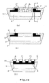
- Fig. 13(a) is a view showing a modification of the first embodiment shown in Figs. 1(a) and 1(b) .
- Reference numeral 42 in Fig. 13(a) indicates a semiconductor device.
- the semiconductor device 42 is different from the semiconductor device 10 shown in Figs. 1(a) and 1(b) in that a dambar 43 is formed much thicker than each of leads 6 in thickness.
- a mold to be used is different from the mold 18 shown in Fig. 3(a) in that as shown in Fig. 13(b) , the depth of a cavity 45 defined in a lower form 44a is deeper than that of the cavity 19 defined in the mold 18 shown in Fig.
- each lead 6 is electrically connected and fixed to a printed board 48 by solder 47 as shown in Fig. 13(c) .
- the thermal expansion coefficient thereof substantially coincides with about 3 x 10 -6 /°C corresponding to a thermal expansion coefficient of silicon.
- the thermal expansion coefficient of the printed board 48 is substantially identical to 2 to 3 x 10 -5 /°C corresponding to a thermal expansion coefficient of a resin.
- the thermal expansion coefficient of the printed board 48 is increased by one digit as compared with the semiconductor device 10.
- the thermal expansion coefficient of the printed board 48 is larger than that of the semiconductor device 10 in this way, a thermal stress produced due to the difference between the thermal expansion coefficients is concentrated on the solder 47 used as each junction between the printed board 48 and the semiconductor device 10 after the implementation of the semiconductor device 10 on the printed board 48.
- the thermal stress increases, cracks are produced in the solder, so that there is a fear that they will result in a conductive failure.
- a substrate composed of ceramic whose thermal expansion coefficient is close to that of the semiconductor element 2 may be used in place of the printed board 48.
- the ceramic substrate is so expensive in this case, a great increase in cost will be incurred.
- the semiconductor device 42 according to the present modification is constructed in such a manner that the dambar 43 is much thicker than each lead 6 in thickness as shown in Fig. 13(a) .
- the semiconductor device 42 is implemented on the printed board 48, grooves 49 corresponding to the positions and configurations of the dambars 43 are defined in predetermined positions on the printed board 48 in advance.
- the dambars 43 of the semiconductor device 42 are respectively fitted in the grooves 49 of the printed board 48 as projections and are connected and fixed to the printed board 48 by the solder 47 in this condition.
- the thermal stress produced due to the difference between the thermal expansion coefficients is reduced by fitting the projections composed of the dambars 43 in their corresponding grooves 49 defined in the printed board 48, whereby cracks can be prevented from occurring in the solder 47.
- the semiconductor device 42 according to the present modification when constructed as a structure in which the semiconductor device 42 is implemented on the board, such a structure can prevent the cracks from occurring in the solder 47 used for fixing the semiconductor device 42. As a result, the electrical connections between the semiconductor device and the printed board by the solder 47 can be kept satisfactory.
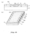
- Fig. 14 is a view showing a second embodiment of the present invention.
- Reference numeral 14 in Fig. 14 indicates a semiconductor device.
- the present semiconductor device 50 is different from the semiconductor device 10 shown in Fig. 1(a) and 1(b) in that surfaces of a semiconductor element 2, which are other than a circuit forming surface 2a thereof are covered with a coating resin.
- the semiconductor device 50 shown in Fig. 14 is provided in such a manner that the surfaces of the semiconductor element 2, other than the circuit forming surface 2a and side end surfaces of an adhesive tape 3 placed on the circuit forming surface 2a are covered with a coating resin 51.
- the coating resin 51 is composed of, for example, an epoxy resin, a polyimide resin or the like and ranges from about 20 ⁇ m to 30 ⁇ m in thickness.
- the coating resin 51 is one coated so as to keep the size of the semiconductor device 50 itself almost constant.
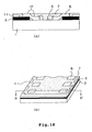
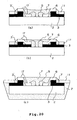
- a process up to mold resin sealing is executed in a manner similar to the manufacturing method shown in Figs. 2 through 4 . Thereafter, the resultant semiconductor device subjected to the resin sealing is immersed into a resin tank 52 fully filled with a liquid resin 51a obtained by dissolving the coating resin 51 in a solvent, as shown in Fig. 15(a) . At this time, the resin-sealed semiconductor device is kept in a state in which each dambar support 14 of a lead frame 12 is not being cut.
- the size of an opening of the resin tank 52 is set to a size in which the dambar supports 14 are suspended at the edges of the resin tank 52 when the semiconductor device is immersed into the resin tank 52.
- the semiconductor element 2 side is immersed into the liquid resin 51a for a suitable time interval as mentioned above in the state in which the dambar supports 14 of the semiconductor device have been suspended at the edges of the resin tank 52.
- the semiconductor device is pulled up from the resin tank 52 and the coating resin attached to the semiconductor device is dried and hardened at a temperature of about 100°C for several hours as shown in Fig. 15(b) .
- the dambar supports 14 are cut in a manner similar to the manufacturing method shown in Figs. 2 through 4 to thereby obtain the semiconductor device 50 shown in Fig. 14 .
- the covering of the surfaces of the semiconductor element 2, other than the circuit forming surface 2a with the coating resin 51 makes it hard to scratch the surfaces upon handling of the semiconductor device 50, for example and improve the resistance of the semiconductor device 50 to an impact.
- the semiconductor element 2 is composed of a brittle material such as silicon or the like, large cracks are produced even if any flaws occur in the surfaces, so that the function of the semiconductor element 2 is apt to be impaired.
- the covering of the surfaces with the coating resin 51 can reduce an external impact so as to prevent the occurrence of the cracks.
- the boundary between the circuit forming surface 2a of the semiconductor element 2a and the back of the adhesive tape 3 is also covered with the coating resin 51 as shown in Fig. 14 , the resistance of the semiconductor device to moisture can be also improved.
- the dambar supports 14 are suspended at the edges of the resin tank 52 fully filled with the liquid resin 51a and the lower side of each dambar support 14 is immersed into the liquid resin 51a before the cutting of the dambar supports 14, resin coating is extremely easy and the fabrication of the semiconductor device 50 does not need a special device. Further, the semiconductor device 50 can be fabricated easily and in full correspondence with its mass productivity.
- Figs. 16(a) and 16(b) are respectively views showing one example of a plastic molded type semiconductor device of the present invention, which is obtained by a method of manufacturing the semiconductor device.
- Reference numerals 60 in Figs. 16(a) and 16(b) indicate a semiconductor device.
- the method of manufacturing the semiconductor device 60 is different from the manufacturing method described with reference to Figs. 2 through 4 in that a lead frame 61 shown in Fig. 17 is used.
- the lead frame 61 comprises a lead frame member 13 and a lead frame body 63 connected to the inside of the lead frame member 13 through a plurality of dambar supports 62.
- the lead frame body 63 comprises a frame-shaped dambar 64 having an outer shape substantially identical to that of a circuit forming surface 2a of a semiconductor element 2, a therein is smaller than the outer shape of a circuit forming surface 2a of a semiconductor element 2. Further, the parts of the leads 6 are bonded to the inner edge of each opening 55a and the remaining parts thereof extend into the opening 55a.
- the adhesive tape 55 is constructed as shown in Fig. 17(c) .
- an adhesive layer 56a is formed on the surface of the adhesive tape 55 on the side of the bonding of each lead 6 to the adhesive tape 55 so as to extend from the inner edge thereof for defining the opening 55a to the position of bonding of each lead 6 to the adhesive tape 55.
- an adhesive layer 56b is formed on the opposed surface of the adhesive tape 55 so as to extend from the inner edge thereof for defining the opening 55a to the position identical to that of the outer edge of the circuit forming surface 2a of the semiconductor element 2.
- an adhesive layer (resin is not shown) is provided at the position of the surface of the adhesive tape 55 on the side of bonding of each lead 6 to the surface thereof, which position corresponds to the lead frame member 13, and no adhesive layer is formed at other locations.
- each lead frame body of the lead frame 54 is placed on the semiconductor element 2 in such a manner that the outer edge of the adhesive layer 56b on the adhesive tape 55 substantially coincide with the outer edge of the circuit forming surface 2a of the semiconductor element 2. Thereafter, the leads 6 are fixed onto the semiconductor element 2 by the adhesive tape 55.
- the leads 6 on the semiconductor element 2 are respectively connected to the circuit forming surface 2a of the semiconductor element 2 by the gold wires 5. Further, the semiconductor element 2 connected with the gold wires 5 is placed in a cavity 58 defined in a mold 57 as shown in Fig. 17(b). As the mold 57, one is used in which a recess or concave portion 58a having a depth equal to the thickness of the semiconductor element 2 is defined in a lower form 57a and an open concave portion 58b being a size smaller than the circuit forming surface 2a is defined in an upper form 57b.
- the mold 57 referred to above is used and a mold resin is charged into the cavity 58 through a resin injection hole 20 in a state in which the outer peripheral portion of the adhesive tape 55 is being interposed between the lower form 57a and the upper form 57b, followed by hardening of the charged resin. Thereafter, the semiconductor element 2 is taken out from the mold 57 to thereby obtain the semiconductor element 2 in which resin sealing has been completed as shown in Fig. 17(c). Further, the adhesive tape 55 extending toward each side of the semiconductor element 2 is cut to obtain the semiconductor device 53 shown in Fig. 16(a) .
- each adhesive layer is provided only at the predetermined position of the adhesive tape 55 for forming each lead frame body, the adhesive tape 55 can be prevented from being cemented to the mold 57 even if the outer peripheral portion of the adhesive tape 55 is interposed between the lower form 57a and upper form 57b of the mold 57 and the mold resin sealing is executed in this condition.
- the resin sealing process can be performed without a hitch, the semiconductor device 53 can be easily manufactured.
- Figs. 18(a) and 18(b) are respectively views showing one example of a plastic molded type semiconductor device of the present invention, which is obtained by a method of manufacturing the semiconductor device.
- Reference numerals 60 in Figs. 18(a) and 18(b) indicate a semiconductor device.
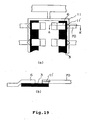
- the method of manufacturing the semiconductor device 60 is different from the manufacturing method described with reference to Figs. 2 through 4 in that a lead frame 61 shown in Fig. 19 is used.
- the lead frame 61 comprises a lead frame member 13 and a lead frame body 63 connected to the inside of the lead frame member 13 through a plurality of dambar supports 62.
- the lead frame body 63 comprises a frame-shaped dambar 64 having an outer shape substantially identical to that of a circuit forming surface 2a of a semiconductor element 2, a plurality of leads 6 extending inwardly of the dambar 64 in continuous or connection with the dambar 64, a lead support 65 for connecting between these leads 6 and 6 and connected to the dambar 64, and an adhesive tape (not shown) bonded to these so as to extend from one surface of the dambar 64 to the course or middle of each lead 6.
- Each resin portion 66 composed of an insulating resin is formed between all the adjacent leads 6 and 6 within the dambar 64 so as to provide electrical discontinuity (non-conduction) between these leads 6 and 6.
- the insulating resin used for the resin portion 66 is the same resin as a mold resin to be filled subsequently.
- the lead frame 61 is different from the lead frame 12 shown in Figs. 2(a) through 2(e) in that the leads 6 are given metal plating (solder plating) after the completion of mold resin sealing as will be described later, without applying metal plating to the leads 6 in the state of the lead frame.
- the lead support 65 is eliminated from the lead frame body 63 in advance. Further, the lead frame body 63 of the lead frame 61 is placed on the circuit forming surface 2a of the semiconductor element 2 in the same manner as the case shown in Figs. 2 through 4 and fixed to the circuit forming surface 2a with the adhesive tape.
- the leads 6 on the semiconductor element 2 and the circuit forming surface 2a of the semiconductor element 2 are electrically connected to each other with gold wires 5. Further, the semiconductor element 2 connected with the gold wires 5 is introduced into a cavity of a mold (not shown). Moreover, the inside of the dambar 64 is filled with the mold resin within the mold to seal the circuit forming surface 2a of the semiconductor element 2. Thereafter, the semiconductor element 2 is taken out from the mold and the leads 6 are given metal plating (solder plating). Further, the dambar supports 62 are cut so as to obtain the semiconductor device 60 shown in Figs. 16(a) and 16(b) .
- the semiconductor device 60 obtained in this way can avoid electrical conduction between the adjacent leads 6 and 6 regardless of the fact that the leads 6 are continuously connected to the dambar 64.
- the leads 6 are respectively electrically connected to the dambar supports 62 through the dambar 64, the leads 6 can be given solder plating by the use of the dambar supports 62 in the same manner as ever.
- Figs. 18(a) and 18(b) are respectively views showing a third embodiment of the present invention.
- a dambar 11 is subjected to half etching at portions adjacent to leads 6 as shown in Figs. 20(a) and 20(b) .
- the half-etched portions are covered with a mold resin 7.
- a dambar 11 is subjected to half etching 11' and supports 70 are formed adjacent to the half-etched portions.
- the supports 70 are used to prevent the half-etched portions 11' from extending out to end surfaces of the dambar 11 and the supports 70.
- the half-etched portions are formed within the planes of both the dambar 11 adjacent to the leads and the supports 70 adjacent thereto.
- the resin is introduced into the half-etched portions. Thereafter, the resin stops flowing at the end surfaces of the dambar 11 and the supports 70.
- the neighborhood of each lead 6 can be covered with the mold resin.
- Figs. 20(a) through 20(c) are respectively views showing applications of a fourth embodiment of the present invention.
- the provision of a steplike offset or a difference in level between a dambar 11 and each lead 6 allows a reduction in electrical leakage produced between the dambar 11 and each lead 6.
- insulating tapes 3 and 3' are provided in double form at leads 6 alone as shown in Figs. 20(a) through 20(c) .
- the thickness of each lead 6 becomes thicknesses of the two insulating tape 3 and 3' and the thickness of the dambar 11 is one insulating tape 3 thick. Therefore, a difference in level corresponding to the insulating tape 3' can be formed between the dambar 11 and each lead 6.
- Fig. 21 is a view for describing a lead frame employed in each application shown in Fig. 20 .
- Fig. 21 (a) is a view showing the manner in which an adhesive tape 3' is bonded to each lead.
- Fig. 21 (b) is a cross-section cut away at each lead in Fig. 21 (a).
- Fig. 21 (c) is a view illustrating the manner in which after the insulating tape 3' has been bonded to each lead, an insulating tape 3 is further cemented thereto and each lead 6 is subjected to bending.
- Fig. 21 (d) is a cross-section cut away at the leads in Fig. 21 (c) .
- a difference in level corresponding to one insulating tape 3' is formed between the dambar 11 and each lead 6 by forming each lead as shown in Fig. 21(d) .
- Figs. 22(a) through 22(c) are respectively views showing a fifth embodiment of the present invention.
- grooves 71 identical in height to a dambar 11 are provided between respective adjacent leads 6.
- Fig. 22(a) is a cross-section cut away at the leads
- Fig. 22(b) is a cross-section cut away at a resin portion
- Fig. 22(c) is a cross-sectional view taken along line C - C' in Fig. 22(a) .
- a difference in level, which corresponds to an insulating tape 3' is provided between the dambar 11 and each lead 6. Further, the grooves 71 identical in height to the dambar 11 are provided between the leads 6. Therefore, electrical leakage produced between the leads 6 and 6 can be reduced as well as electrical leakage produced between the dambar and each leak due to impurities.
Landscapes
- Encapsulation Of And Coatings For Semiconductor Or Solid State Devices (AREA)
- Structures Or Materials For Encapsulating Or Coating Semiconductor Devices Or Solid State Devices (AREA)
Claims (17)
- Dispositif semi-conducteur (10) de type moulé en plastique ou en résine comprenant :un élément semi-conducteur (2) ayant des électrodes disposées sur une de ses surfaces (2a) ;une pluralité de conducteurs (6) respectivement connectés électriquement audites électrodes ; etun matériau de scellement (7) formé de manière à sceller la surface dudit élément semi-conducteur (2) et à exposer des parties desdits conducteurs (6) ;
caractérisé par :une barrière de blocage (11) formée le long de la périphérie extérieure de la surface (2a) dudit élément semi-conducteur (2) ;
dans lequel :ladite pluralité de conducteurs (6) est disposée à l'intérieur de la barrière de blocage (11) électriquement indépendants de ladite barrière de blocage (11) ;ladite barrière de blocage (11) et lesdits contacteurs (6) sont fixés les uns aux autres avec une bande adhésive isolante (3) ; etledit matériau de scellement (7) est formée dans une région entourée par ladite barrière de blocage (11). - Dispositif semi-conducteur (10) selon la revendication 1, dans lequel ladite barrière de blocage (11) et lesdits conducteurs (6) sont fixés audit élément semi-conducteur (2) par une bande isolante.
- Dispositif semi-conducteur (42) selon la revendication 1, dans lequel l'épaisseur de ladite barrière de blocage (43) est plus grande que celle de chaque conducteur (6).
- Dispositif semi-conducteur (50) selon la revendication 1, dans lequel le coté et le dos dudit élément semi-conducteur (2) sont recouverts avec une résine de revêtement (51).
- Dispositif semi-conducteur (10) selon la revendication 1, comprenant :un matériau de fixation pour fixer ladite barrière de blocage (11) et lesdits conducteurs (6) sur la surface (2a) dudit élément semi-conducteur (2) ;
dans lequel ladite barrière de blocage (11) a des parties correspondantes auxdits conducteurs (6), qui sont formées plus minces que d'autres portions de celle-ci, et qui sont équipées de supports (14) identiques en épaisseur auxdites autres parties autour des parties formées minces. - Dispositif semi-conducteur (10) selon la revendication 5, dans lequel les parties de ladite barrière de blocage (11), qui sont formées plus minces que les autres parties de celle-ci, sont remplies avec le matériau de scellement (7).
- Dispositif semi-conducteur selon la revendication 5, dans lequel les parties desdits conducteurs (6) et ladite barrière de blocage (11) sont formées de telle manière que leurs surfaces supérieures sont substantiellement sans aspérité l'une par rapport à l'autre.
- Procédé de fabrication d'un dispositif semi-conducteur (10) de type moulé en plastique ou en résine, comprenant les étapes suivantes :une étape pour préparer des éléments semi-conducteurs (2) chacun ayant des électrodes disposées sur une de leur surface (2a) ;une étape destinée à former une grille de connexion (12) possédant des barrières de blocage (11) en forme de grille ayant une forme extérieure substantiellement identique à celle de la surface (2a) d'un des éléments semi-conducteurs respectifs (2) et une pluralité de conducteurs (6) disposés à l'intérieur de chacune des barrières de blocage (11) et électriquement indépendants de celles-ci, chacune desdites barrières de blocage (11) et ses conducteurs respectifs (6) étant fixés les uns aux autres avec une bande adhésive isolante (3) ;une étape destinée à placer ladite grille de connexion (12) sur la surface (2a) dudit chacun desdits éléments semi-conducteurs (2) de telle sorte que chacune desdites barrières de blocage (11) coïncide substantiellement en bordure extérieure avec la surface (2a) dudit élément semi-conducteur (2) respectif et à fixer lesdits conducteurs (6) et lesdites barrières de blocage (11) sur ledit élément semi-conducteur (2) respectif avec la bande adhésive (3) ;une étape destinée à connecter électriquement lesdits conducteurs (6) et lesdits éléments semi-conducteurs respectifs (2) les uns aux autres avec des fils conducteurs (5) ; etune étape destinée à remplir l'intérieur de chacune desdites barrières de blocage (11) avec un matériau de scellement (7) à l'intérieur d'un moule de manière à sceller les surfaces (2a) dudit élément semi-conducteur (2) et à exposer des parties desdits conducteurs respectifs (6).
- Procédé selon la revendication 8, dans lequel ladite bande adhésive (3) est formée de manière à ce que la forme extérieure soit substantiellement identique à la surface (2a) desdits éléments semi-conducteurs respectifs (2) avec ladite bande adhésive collée à elle (3) et est formée de manière à être légèrement plus large que les surfaces (2a) desdits éléments semi-conducteurs respectifs (2) en dimension extérieure, dans lequel chacune desdites barrières de blocage (11) est formée de manière à être légèrement plus large que la bande adhésive (3) en dimension extérieure, et ladite bande adhésive (3) est collée à chacune desdites barrières de blocage (11) de telle manière que ladite bande adhésive (3) coïncide substantiellement en bordure extérieure avec lesdites barrières de blocage (11).
- Procédé selon la revendication 8, dans lequel chacune desdites barrières de blocage (11) a des supports de barrière de blocage (14) respectifs s'étendant à partir de celles-ci et des rainures s'étendant à partir des bordures internes desdites barrières de blocage (11) jusqu'aux bordures conductrices desdits supports de barrière de blocage (14), lesdits rainures étant définies dans des surfaces de parties desdits supports de barrière de blocage (14) et lesdites barrières de blocage (11) étant connectées de façon continue auxdits supports de barrière de blocage (14) sur le côté opposé à ladite bande adhésive (3).
- Procédé selon la revendication 8, dans lequel ladite grille de connexion (12) a une pluralité de corps de grille de connexion (15) et de conducteurs de barrière de blocage à barrière de blocage (24) pour connecter les barrières de blocage entre elles, des rainures (22) s'étendant à partir des bordures intérieures d'une desdites barrières de blocage (11) jusqu'à une bordure intérieure d'une autre desdites barrières de blocage (11) au moyen desdits conducteurs de barrière de blocage à barrière de blocage (24), lesdites rainures (22) étant définies sur des premières surfaces de parties de chacun desdits conducteurs de barrière de blocage à barrière de blocage (24) et chacune desdites barrières de blocage (11) étant connectée de façon continue à celle-ci sur le côté opposé à ladite bande adhésive (3), et des trous communiquant avec lesdites rainures (22), qui sont respectivement définis dans des secondes surfaces, différentes desdites premières surfaces desdits conducteurs de barrière de blocage à barrière de blocage (24), et ladite étape destinée à charger le matériau de scellement (7) de manière à sceller les surfaces (2a) desdits éléments semi-conducteurs (2) connectés avec lesdits conducteurs (6) est exécutée dans un état dans lequel ladite grille de connexion (12) a été fixée sur les éléments semi-conducteurs (12), les éléments semi-conducteurs (12) et les corps de grille de connexion (15) de ladite grille de connexion (12) étant en nombre identiques.
- Procédé selon la revendication 8, dans lequel ladite étape destinée à remplir l'intérieur desdites barrières de blocage (11) avec le matériau de scellement à l'intérieur du moule de manière à sceller les surfaces (2a) desdits éléments semi-conducteurs (2) avec lesdits conducteurs (6) connectés à celles-ci utilise un moule dans lequel des parties concaves sont définies dans une face inférieure pour former une cavité, et est exécutée dans un état dans lequel des surfaces desdits éléments semi-conducteurs (2) sur les côtés opposés desdites surfaces (2a) avec lesdits conducteurs (6) connecté à celles-ci ont été amenées en contact avec ladite face inférieure.
- Procédé selon la revendication 12, dans lequel lesdites parties concaves définies dans ladite face inférieure sont formées par des surfaces convexes obtenues en étendant leurs surfaces concaves vers le bas de la face inférieure.
- Procédé selon la revendication 12 ou 13, dans lequel lesdites parties concaves définies dans ladite face inférieure sont respectivement formées de manière symétrique ou disposées dans leurs directions orientées vers le haut et vers le bas et leur direction vers la droite et vers la gauche à partir de la forme de la face inférieure telle que vue dans le plan de celle-ci.
- Procédé selon la revendication 8, dans lequel la grille de connexion préparée a des supports de barrière de blocage, chacun étant attaché à chaque barrière de blocage (11) et s'étendant vers l'extérieur de la barrière de blocage et ledit chaque support de barrière de blocage comprend une partie connectée de façon continue à la barrière de blocage (11) et plus mince que la barrière de blocage en épaisseur et une partie connectée de façon continue à la partie à paroi mince et identique en épaisseur à la barrière de blocage.
- Procédé selon la revendication 8, dans lequel la grille de connexion préparée a des supports de barrière de blocage respectivement disposés à des intervalles distants des barrières de blocage (11) et s'étendant vers l'extérieure de celles-ci, ledit chaque supports de barrière de blocage (14) étant connecté à la barrière de blocage (11) avec une bande adhésive (3).
- Procédé selon la revendication 8, comprenant :une étape destinée à préparer une grille de connexion (12) composée des barrières de blocage (11), chaque barrière de blocage (11) ayant une forme extérieure substantiellement identique à celle de la surface (2a) d'un des éléments semi-conducteurs respectifs (2), et des conducteurs supplémentaires (6) étant disposés à l'intérieur de ladite chaque barrière de blocage supplémentaires (11), dans un état consistant à être hors de contact avec lesdites barrières de blocage (11), et des bandes adhésives isolantes (3) collées à des parties desdits conducteurs supplémentaires (6) et lesdites barrières de blocage (11) au dessus des surfaces de celles-ci sur le même côté desdits conducteurs supplémentaires (6) et auxdites barrières de blocage (11) pour connecter de ce fait les parties desdits conducteurs supplémentaires (6) et desdites barrières de blocage (11) les une aux autres ; etune étape destinée à immerger le côté situé en dessous de la surface supérieure de la bande adhésive (3) sur chacun desdits éléments semi-conducteurs (2) dans une résine de revêtement liquide après l'achèvement du remplissage dudit matériau de scellement, retirer le dispositif semi-conducteur (10) après son immersion et sécher et durcir la résine de revêtement fixée.
Priority Applications (1)
| Application Number | Priority Date | Filing Date | Title |
|---|---|---|---|
| EP20030077346 EP1406299A1 (fr) | 1996-05-16 | 1997-04-29 | Dispositif semi-conducteur moulé dans du plastique et son procédé de fabrication |
Applications Claiming Priority (6)
| Application Number | Priority Date | Filing Date | Title |
|---|---|---|---|
| JP121196/96 | 1996-05-16 | ||
| JP12119696 | 1996-05-16 | ||
| JP12119696 | 1996-05-16 | ||
| JP27601896A JP3427874B2 (ja) | 1996-05-16 | 1996-10-18 | 樹脂封止型半導体装置とその製造方法 |
| JP27601896 | 1996-10-18 | ||
| JP276018/96 | 1996-10-18 |
Related Child Applications (2)
| Application Number | Title | Priority Date | Filing Date |
|---|---|---|---|
| EP20030077346 Division EP1406299A1 (fr) | 1996-05-16 | 1997-04-29 | Dispositif semi-conducteur moulé dans du plastique et son procédé de fabrication |
| EP03077346.9 Division-Into | 2003-07-25 |
Publications (3)
| Publication Number | Publication Date |
|---|---|
| EP0807973A2 EP0807973A2 (fr) | 1997-11-19 |
| EP0807973A3 EP0807973A3 (fr) | 1999-08-04 |
| EP0807973B1 true EP0807973B1 (fr) | 2010-06-02 |
Family
ID=26458614
Family Applications (2)
| Application Number | Title | Priority Date | Filing Date |
|---|---|---|---|
| EP97302914A Expired - Lifetime EP0807973B1 (fr) | 1996-05-16 | 1997-04-29 | Dispositif semi-conducteur du type à incapsulation en plastique et procédé de fabrication |
| EP20030077346 Withdrawn EP1406299A1 (fr) | 1996-05-16 | 1997-04-29 | Dispositif semi-conducteur moulé dans du plastique et son procédé de fabrication |
Family Applications After (1)
| Application Number | Title | Priority Date | Filing Date |
|---|---|---|---|
| EP20030077346 Withdrawn EP1406299A1 (fr) | 1996-05-16 | 1997-04-29 | Dispositif semi-conducteur moulé dans du plastique et son procédé de fabrication |
Country Status (7)
| Country | Link |
|---|---|
| US (1) | US5877542A (fr) |
| EP (2) | EP0807973B1 (fr) |
| JP (1) | JP3427874B2 (fr) |
| KR (1) | KR100346671B1 (fr) |
| CN (1) | CN1162905C (fr) |
| DE (1) | DE69739897D1 (fr) |
| TW (1) | TW334605B (fr) |
Families Citing this family (13)
| Publication number | Priority date | Publication date | Assignee | Title |
|---|---|---|---|---|
| US6336973B1 (en) | 1997-08-05 | 2002-01-08 | Micron Technology, Inc. | Apparatus and method for modifying the configuration of an exposed surface of a viscous fluid |
| US6013535A (en) * | 1997-08-05 | 2000-01-11 | Micron Technology, Inc. | Method for applying adhesives to a lead frame |
| US6040205A (en) * | 1997-08-05 | 2000-03-21 | Micron Technology, Inc. | Apparatus and method for controlling the depth of immersion of a semiconductor element in an exposed surface of a viscous fluid |
| JP3169072B2 (ja) | 1998-05-15 | 2001-05-21 | 日本電気株式会社 | 半導体装置 |
| JP2000156435A (ja) * | 1998-06-22 | 2000-06-06 | Fujitsu Ltd | 半導体装置及びその製造方法 |
| JP3784597B2 (ja) * | 1999-12-27 | 2006-06-14 | 沖電気工業株式会社 | 封止樹脂及び樹脂封止型半導体装置 |
| US6457224B1 (en) | 2000-08-21 | 2002-10-01 | Advanced Micro Devices, Inc. | Dambar punch setup jig |
| JP2002092575A (ja) * | 2000-09-19 | 2002-03-29 | Mitsubishi Electric Corp | 小型カードとその製造方法 |
| US6707135B2 (en) * | 2000-11-28 | 2004-03-16 | Texas Instruments Incorporated | Semiconductor leadframe for staggered board attach |
| TWI246175B (en) * | 2004-10-11 | 2005-12-21 | Ind Tech Res Inst | Bonding structure of device packaging |
| US7989933B1 (en) * | 2008-10-06 | 2011-08-02 | Amkor Technology, Inc. | Increased I/O leadframe and semiconductor device including same |
| JP5208099B2 (ja) | 2009-12-11 | 2013-06-12 | 日立オートモティブシステムズ株式会社 | 流量センサとその製造方法、及び流量センサモジュール |
| CN102104013B (zh) * | 2010-11-10 | 2013-06-12 | 华为终端有限公司 | 数据卡的组装方法及数据卡 |
Family Cites Families (8)
| Publication number | Priority date | Publication date | Assignee | Title |
|---|---|---|---|---|
| US5583375A (en) * | 1990-06-11 | 1996-12-10 | Hitachi, Ltd. | Semiconductor device with lead structure within the planar area of the device |
| JP2895920B2 (ja) * | 1990-06-11 | 1999-05-31 | 株式会社日立製作所 | 半導体装置及びその製造方法 |
| JP2934357B2 (ja) * | 1992-10-20 | 1999-08-16 | 富士通株式会社 | 半導体装置 |
| KR0152901B1 (ko) * | 1993-06-23 | 1998-10-01 | 문정환 | 플라스틱 반도체 패키지 및 그 제조방법 |
| JP3146849B2 (ja) * | 1994-05-27 | 2001-03-19 | 松下電器産業株式会社 | 電子部品および電子部品の製造方法 |
| JPH08222681A (ja) * | 1995-02-14 | 1996-08-30 | Toshiba Corp | 樹脂封止型半導体装置 |
| TW314650B (fr) * | 1995-06-21 | 1997-09-01 | Oki Electric Ind Co Ltd | |
| KR0169820B1 (ko) * | 1995-08-22 | 1999-01-15 | 김광호 | 금속 회로 기판을 갖는 칩 스케일 패키지 |
-
1996
- 1996-10-18 JP JP27601896A patent/JP3427874B2/ja not_active Expired - Fee Related
-
1997
- 1997-04-17 TW TW086105000A patent/TW334605B/zh not_active IP Right Cessation
- 1997-04-24 US US08/847,980 patent/US5877542A/en not_active Expired - Fee Related
- 1997-04-29 DE DE69739897T patent/DE69739897D1/de not_active Expired - Lifetime
- 1997-04-29 EP EP97302914A patent/EP0807973B1/fr not_active Expired - Lifetime
- 1997-04-29 EP EP20030077346 patent/EP1406299A1/fr not_active Withdrawn
- 1997-05-16 CN CNB971110425A patent/CN1162905C/zh not_active Expired - Fee Related
- 1997-05-16 KR KR1019970018825A patent/KR100346671B1/ko not_active Expired - Fee Related
Also Published As
| Publication number | Publication date |
|---|---|
| TW334605B (en) | 1998-06-21 |
| US5877542A (en) | 1999-03-02 |
| JPH1032287A (ja) | 1998-02-03 |
| EP0807973A3 (fr) | 1999-08-04 |
| EP1406299A1 (fr) | 2004-04-07 |
| EP0807973A2 (fr) | 1997-11-19 |
| KR19980032123A (ko) | 1998-07-25 |
| CN1162905C (zh) | 2004-08-18 |
| DE69739897D1 (de) | 2010-07-15 |
| CN1171627A (zh) | 1998-01-28 |
| KR100346671B1 (ko) | 2002-09-18 |
| JP3427874B2 (ja) | 2003-07-22 |
Similar Documents
| Publication | Publication Date | Title |
|---|---|---|
| US6537856B2 (en) | Method of attaching a semiconductor chip to a leadframe with a footprint of about the same size as the chip and packages formed thereby | |
| KR100918745B1 (ko) | 반도체 장치 및 그 제조 방법 | |
| US5864174A (en) | Semiconductor device having a die pad structure for preventing cracks in a molding resin | |
| US5891758A (en) | Semiconductor device and method for manufacturing semiconductor device | |
| JP2842355B2 (ja) | パッケージ | |
| US6627976B1 (en) | Leadframe for semiconductor package and mold for molding the same | |
| EP0807973B1 (fr) | Dispositif semi-conducteur du type à incapsulation en plastique et procédé de fabrication | |
| US5646829A (en) | Resin sealing type semiconductor device having fixed inner leads | |
| JPH0783036B2 (ja) | キヤリアテープ | |
| US6861735B2 (en) | Resin molded type semiconductor device and a method of manufacturing the same | |
| KR100366111B1 (ko) | 수지봉합형 반도체장치의 구조 | |
| US8274125B2 (en) | Semiconductor device and semiconductor device manufacturing method | |
| JP3226244B2 (ja) | 樹脂封止型半導体装置 | |
| US20030102545A1 (en) | Semiconductor device | |
| US20070257345A1 (en) | Package structure to reduce warpage | |
| US7646095B2 (en) | Semiconductor device | |
| US5952710A (en) | Semiconductor device and method of manufacturing same | |
| JPH06342816A (ja) | 半導体装置及びその製造方法並びにそれらに用いるリードフレーム | |
| KR940011380B1 (ko) | 반도체 리드 프레임 | |
| KR100279252B1 (ko) | 세라믹패키지 | |
| KR100221918B1 (ko) | 칩 스케일 패키지 | |
| KR100258852B1 (ko) | 반도체 패키지의 제조 방법 | |
| KR100268925B1 (ko) | 리드프레임및이를이용한반도체패키지 | |
| KR0152574B1 (ko) | 단차 가공된 다이 패드 부분을 갖는 리드 프레임 | |
| KR100253708B1 (ko) | 반도체 패키지 및 그 제조방법 |
Legal Events
| Date | Code | Title | Description |
|---|---|---|---|
| PUAI | Public reference made under article 153(3) epc to a published international application that has entered the european phase |
Free format text: ORIGINAL CODE: 0009012 |
|
| AK | Designated contracting states |
Kind code of ref document: A2 Designated state(s): DE FR GB NL |
|
| PUAL | Search report despatched |
Free format text: ORIGINAL CODE: 0009013 |
|
| AK | Designated contracting states |
Kind code of ref document: A3 Designated state(s): DE FR GB NL |
|
| 17P | Request for examination filed |
Effective date: 19991206 |
|
| 17Q | First examination report despatched |
Effective date: 20030310 |
|
| GRAP | Despatch of communication of intention to grant a patent |
Free format text: ORIGINAL CODE: EPIDOSNIGR1 |
|
| GRAS | Grant fee paid |
Free format text: ORIGINAL CODE: EPIDOSNIGR3 |
|
| GRAA | (expected) grant |
Free format text: ORIGINAL CODE: 0009210 |
|
| GRAL | Information related to payment of fee for publishing/printing deleted |
Free format text: ORIGINAL CODE: EPIDOSDIGR3 |
|
| GRAS | Grant fee paid |
Free format text: ORIGINAL CODE: EPIDOSNIGR3 |
|
| AK | Designated contracting states |
Kind code of ref document: B1 Designated state(s): DE FR GB NL |
|
| REG | Reference to a national code |
Ref country code: GB Ref legal event code: FG4D |
|
| REF | Corresponds to: |
Ref document number: 69739897 Country of ref document: DE Date of ref document: 20100715 Kind code of ref document: P |
|
| REG | Reference to a national code |
Ref country code: NL Ref legal event code: T3 |
|
| PLBE | No opposition filed within time limit |
Free format text: ORIGINAL CODE: 0009261 |
|
| STAA | Information on the status of an ep patent application or granted ep patent |
Free format text: STATUS: NO OPPOSITION FILED WITHIN TIME LIMIT |
|
| 26N | No opposition filed |
Effective date: 20110303 |
|
| REG | Reference to a national code |
Ref country code: DE Ref legal event code: R097 Ref document number: 69739897 Country of ref document: DE Effective date: 20110302 |
|
| REG | Reference to a national code |
Ref country code: NL Ref legal event code: V1 Effective date: 20111101 |
|
| GBPC | Gb: european patent ceased through non-payment of renewal fee |
Effective date: 20110429 |
|
| REG | Reference to a national code |
Ref country code: FR Ref legal event code: ST Effective date: 20111230 |
|
| PG25 | Lapsed in a contracting state [announced via postgrant information from national office to epo] |
Ref country code: NL Free format text: LAPSE BECAUSE OF NON-PAYMENT OF DUE FEES Effective date: 20111101 Ref country code: DE Free format text: LAPSE BECAUSE OF NON-PAYMENT OF DUE FEES Effective date: 20111101 Ref country code: FR Free format text: LAPSE BECAUSE OF NON-PAYMENT OF DUE FEES Effective date: 20110502 |
|
| REG | Reference to a national code |
Ref country code: DE Ref legal event code: R119 Ref document number: 69739897 Country of ref document: DE Effective date: 20111101 |
|
| PG25 | Lapsed in a contracting state [announced via postgrant information from national office to epo] |
Ref country code: GB Free format text: LAPSE BECAUSE OF NON-PAYMENT OF DUE FEES Effective date: 20110429 |