EP0807694B1 - Aufdampfungskammer und Verfahren zur Herstellung eines Films mit einer niedrigen Dielektrizitätskonstante - Google Patents
Aufdampfungskammer und Verfahren zur Herstellung eines Films mit einer niedrigen Dielektrizitätskonstante Download PDFInfo
- Publication number
- EP0807694B1 EP0807694B1 EP97107815A EP97107815A EP0807694B1 EP 0807694 B1 EP0807694 B1 EP 0807694B1 EP 97107815 A EP97107815 A EP 97107815A EP 97107815 A EP97107815 A EP 97107815A EP 0807694 B1 EP0807694 B1 EP 0807694B1
- Authority
- EP
- European Patent Office
- Prior art keywords
- process gas
- chamber
- gas
- substrate
- oxygen
- Prior art date
- Legal status (The legal status is an assumption and is not a legal conclusion. Google has not performed a legal analysis and makes no representation as to the accuracy of the status listed.)
- Expired - Lifetime
Links
- 238000000034 method Methods 0.000 title claims abstract description 56
- 230000008021 deposition Effects 0.000 title claims abstract description 38
- 239000007789 gas Substances 0.000 claims abstract description 119
- 239000000758 substrate Substances 0.000 claims abstract description 65
- QVGXLLKOCUKJST-UHFFFAOYSA-N atomic oxygen Chemical compound [O] QVGXLLKOCUKJST-UHFFFAOYSA-N 0.000 claims abstract description 52
- 239000001301 oxygen Substances 0.000 claims abstract description 52
- 229910052760 oxygen Inorganic materials 0.000 claims abstract description 52
- BLRPTPMANUNPDV-UHFFFAOYSA-N Silane Chemical compound [SiH4] BLRPTPMANUNPDV-UHFFFAOYSA-N 0.000 claims abstract description 46
- 238000000151 deposition Methods 0.000 claims abstract description 42
- 229910000077 silane Inorganic materials 0.000 claims abstract description 42
- ABTOQLMXBSRXSM-UHFFFAOYSA-N silicon tetrafluoride Chemical compound F[Si](F)(F)F ABTOQLMXBSRXSM-UHFFFAOYSA-N 0.000 claims abstract description 37
- 230000008569 process Effects 0.000 claims abstract description 35
- 239000000203 mixture Substances 0.000 claims abstract description 9
- 239000012530 fluid Substances 0.000 claims description 6
- 230000037361 pathway Effects 0.000 claims description 6
- 230000001939 inductive effect Effects 0.000 claims description 3
- 229910004014 SiF4 Inorganic materials 0.000 abstract 2
- 239000010408 film Substances 0.000 description 20
- XKRFYHLGVUSROY-UHFFFAOYSA-N Argon Chemical compound [Ar] XKRFYHLGVUSROY-UHFFFAOYSA-N 0.000 description 10
- XUIMIQQOPSSXEZ-UHFFFAOYSA-N Silicon Chemical compound [Si] XUIMIQQOPSSXEZ-UHFFFAOYSA-N 0.000 description 5
- 229910052786 argon Inorganic materials 0.000 description 5
- 229910052710 silicon Inorganic materials 0.000 description 5
- 239000010703 silicon Substances 0.000 description 5
- 238000012360 testing method Methods 0.000 description 5
- YCKRFDGAMUMZLT-UHFFFAOYSA-N Fluorine atom Chemical compound [F] YCKRFDGAMUMZLT-UHFFFAOYSA-N 0.000 description 4
- 238000006243 chemical reaction Methods 0.000 description 4
- 238000005229 chemical vapour deposition Methods 0.000 description 4
- 229910052731 fluorine Inorganic materials 0.000 description 4
- 239000011737 fluorine Substances 0.000 description 4
- 238000004544 sputter deposition Methods 0.000 description 4
- 238000002347 injection Methods 0.000 description 3
- 239000007924 injection Substances 0.000 description 3
- 239000004065 semiconductor Substances 0.000 description 3
- BOTDANWDWHJENH-UHFFFAOYSA-N Tetraethyl orthosilicate Chemical compound CCO[Si](OCC)(OCC)OCC BOTDANWDWHJENH-UHFFFAOYSA-N 0.000 description 2
- 230000032683 aging Effects 0.000 description 2
- 238000004590 computer program Methods 0.000 description 2
- 239000004020 conductor Substances 0.000 description 2
- 230000002939 deleterious effect Effects 0.000 description 2
- 230000001419 dependent effect Effects 0.000 description 2
- 230000000694 effects Effects 0.000 description 2
- 238000005530 etching Methods 0.000 description 2
- 239000011521 glass Substances 0.000 description 2
- 229920001296 polysiloxane Polymers 0.000 description 2
- 239000000126 substance Substances 0.000 description 2
- 230000002411 adverse Effects 0.000 description 1
- 230000008901 benefit Effects 0.000 description 1
- 230000015572 biosynthetic process Effects 0.000 description 1
- -1 chamber pressure Substances 0.000 description 1
- 230000008859 change Effects 0.000 description 1
- 238000012993 chemical processing Methods 0.000 description 1
- 238000004891 communication Methods 0.000 description 1
- 238000005137 deposition process Methods 0.000 description 1
- 238000013461 design Methods 0.000 description 1
- 230000006866 deterioration Effects 0.000 description 1
- 239000003989 dielectric material Substances 0.000 description 1
- 238000009826 distribution Methods 0.000 description 1
- 150000002222 fluorine compounds Chemical class 0.000 description 1
- 230000006872 improvement Effects 0.000 description 1
- 238000004519 manufacturing process Methods 0.000 description 1
- 239000000463 material Substances 0.000 description 1
- 230000004048 modification Effects 0.000 description 1
- 238000012986 modification Methods 0.000 description 1
- 238000005268 plasma chemical vapour deposition Methods 0.000 description 1
- 238000012545 processing Methods 0.000 description 1
- 239000000376 reactant Substances 0.000 description 1
- 230000009257 reactivity Effects 0.000 description 1
- 230000009467 reduction Effects 0.000 description 1
- 230000000717 retained effect Effects 0.000 description 1
- 238000009991 scouring Methods 0.000 description 1
- 238000007789 sealing Methods 0.000 description 1
- 239000004460 silage Substances 0.000 description 1
- 238000002230 thermal chemical vapour deposition Methods 0.000 description 1
- 239000010409 thin film Substances 0.000 description 1
- 239000012780 transparent material Substances 0.000 description 1
- 238000009827 uniform distribution Methods 0.000 description 1
- 238000005406 washing Methods 0.000 description 1
Images


Classifications
-
- H01L21/205—
-
- C—CHEMISTRY; METALLURGY
- C23—COATING METALLIC MATERIAL; COATING MATERIAL WITH METALLIC MATERIAL; CHEMICAL SURFACE TREATMENT; DIFFUSION TREATMENT OF METALLIC MATERIAL; COATING BY VACUUM EVAPORATION, BY SPUTTERING, BY ION IMPLANTATION OR BY CHEMICAL VAPOUR DEPOSITION, IN GENERAL; INHIBITING CORROSION OF METALLIC MATERIAL OR INCRUSTATION IN GENERAL
- C23C—COATING METALLIC MATERIAL; COATING MATERIAL WITH METALLIC MATERIAL; SURFACE TREATMENT OF METALLIC MATERIAL BY DIFFUSION INTO THE SURFACE, BY CHEMICAL CONVERSION OR SUBSTITUTION; COATING BY VACUUM EVAPORATION, BY SPUTTERING, BY ION IMPLANTATION OR BY CHEMICAL VAPOUR DEPOSITION, IN GENERAL
- C23C16/00—Chemical coating by decomposition of gaseous compounds, without leaving reaction products of surface material in the coating, i.e. chemical vapour deposition [CVD] processes
- C23C16/44—Chemical coating by decomposition of gaseous compounds, without leaving reaction products of surface material in the coating, i.e. chemical vapour deposition [CVD] processes characterised by the method of coating
- C23C16/455—Chemical coating by decomposition of gaseous compounds, without leaving reaction products of surface material in the coating, i.e. chemical vapour deposition [CVD] processes characterised by the method of coating characterised by the method used for introducing gases into reaction chamber or for modifying gas flows in reaction chamber
- C23C16/45563—Gas nozzles
- C23C16/45574—Nozzles for more than one gas
-
- C—CHEMISTRY; METALLURGY
- C23—COATING METALLIC MATERIAL; COATING MATERIAL WITH METALLIC MATERIAL; CHEMICAL SURFACE TREATMENT; DIFFUSION TREATMENT OF METALLIC MATERIAL; COATING BY VACUUM EVAPORATION, BY SPUTTERING, BY ION IMPLANTATION OR BY CHEMICAL VAPOUR DEPOSITION, IN GENERAL; INHIBITING CORROSION OF METALLIC MATERIAL OR INCRUSTATION IN GENERAL
- C23C—COATING METALLIC MATERIAL; COATING MATERIAL WITH METALLIC MATERIAL; SURFACE TREATMENT OF METALLIC MATERIAL BY DIFFUSION INTO THE SURFACE, BY CHEMICAL CONVERSION OR SUBSTITUTION; COATING BY VACUUM EVAPORATION, BY SPUTTERING, BY ION IMPLANTATION OR BY CHEMICAL VAPOUR DEPOSITION, IN GENERAL
- C23C16/00—Chemical coating by decomposition of gaseous compounds, without leaving reaction products of surface material in the coating, i.e. chemical vapour deposition [CVD] processes
- C23C16/22—Chemical coating by decomposition of gaseous compounds, without leaving reaction products of surface material in the coating, i.e. chemical vapour deposition [CVD] processes characterised by the deposition of inorganic material, other than metallic material
- C23C16/30—Deposition of compounds, mixtures or solid solutions, e.g. borides, carbides, nitrides
- C23C16/40—Oxides
- C23C16/401—Oxides containing silicon
-
- C—CHEMISTRY; METALLURGY
- C23—COATING METALLIC MATERIAL; COATING MATERIAL WITH METALLIC MATERIAL; CHEMICAL SURFACE TREATMENT; DIFFUSION TREATMENT OF METALLIC MATERIAL; COATING BY VACUUM EVAPORATION, BY SPUTTERING, BY ION IMPLANTATION OR BY CHEMICAL VAPOUR DEPOSITION, IN GENERAL; INHIBITING CORROSION OF METALLIC MATERIAL OR INCRUSTATION IN GENERAL
- C23C—COATING METALLIC MATERIAL; COATING MATERIAL WITH METALLIC MATERIAL; SURFACE TREATMENT OF METALLIC MATERIAL BY DIFFUSION INTO THE SURFACE, BY CHEMICAL CONVERSION OR SUBSTITUTION; COATING BY VACUUM EVAPORATION, BY SPUTTERING, BY ION IMPLANTATION OR BY CHEMICAL VAPOUR DEPOSITION, IN GENERAL
- C23C16/00—Chemical coating by decomposition of gaseous compounds, without leaving reaction products of surface material in the coating, i.e. chemical vapour deposition [CVD] processes
- C23C16/44—Chemical coating by decomposition of gaseous compounds, without leaving reaction products of surface material in the coating, i.e. chemical vapour deposition [CVD] processes characterised by the method of coating
- C23C16/455—Chemical coating by decomposition of gaseous compounds, without leaving reaction products of surface material in the coating, i.e. chemical vapour deposition [CVD] processes characterised by the method of coating characterised by the method used for introducing gases into reaction chamber or for modifying gas flows in reaction chamber
- C23C16/45512—Premixing before introduction in the reaction chamber
-
- C—CHEMISTRY; METALLURGY
- C23—COATING METALLIC MATERIAL; COATING MATERIAL WITH METALLIC MATERIAL; CHEMICAL SURFACE TREATMENT; DIFFUSION TREATMENT OF METALLIC MATERIAL; COATING BY VACUUM EVAPORATION, BY SPUTTERING, BY ION IMPLANTATION OR BY CHEMICAL VAPOUR DEPOSITION, IN GENERAL; INHIBITING CORROSION OF METALLIC MATERIAL OR INCRUSTATION IN GENERAL
- C23C—COATING METALLIC MATERIAL; COATING MATERIAL WITH METALLIC MATERIAL; SURFACE TREATMENT OF METALLIC MATERIAL BY DIFFUSION INTO THE SURFACE, BY CHEMICAL CONVERSION OR SUBSTITUTION; COATING BY VACUUM EVAPORATION, BY SPUTTERING, BY ION IMPLANTATION OR BY CHEMICAL VAPOUR DEPOSITION, IN GENERAL
- C23C16/00—Chemical coating by decomposition of gaseous compounds, without leaving reaction products of surface material in the coating, i.e. chemical vapour deposition [CVD] processes
- C23C16/44—Chemical coating by decomposition of gaseous compounds, without leaving reaction products of surface material in the coating, i.e. chemical vapour deposition [CVD] processes characterised by the method of coating
- C23C16/455—Chemical coating by decomposition of gaseous compounds, without leaving reaction products of surface material in the coating, i.e. chemical vapour deposition [CVD] processes characterised by the method of coating characterised by the method used for introducing gases into reaction chamber or for modifying gas flows in reaction chamber
- C23C16/45514—Mixing in close vicinity to the substrate
-
- C—CHEMISTRY; METALLURGY
- C23—COATING METALLIC MATERIAL; COATING MATERIAL WITH METALLIC MATERIAL; CHEMICAL SURFACE TREATMENT; DIFFUSION TREATMENT OF METALLIC MATERIAL; COATING BY VACUUM EVAPORATION, BY SPUTTERING, BY ION IMPLANTATION OR BY CHEMICAL VAPOUR DEPOSITION, IN GENERAL; INHIBITING CORROSION OF METALLIC MATERIAL OR INCRUSTATION IN GENERAL
- C23C—COATING METALLIC MATERIAL; COATING MATERIAL WITH METALLIC MATERIAL; SURFACE TREATMENT OF METALLIC MATERIAL BY DIFFUSION INTO THE SURFACE, BY CHEMICAL CONVERSION OR SUBSTITUTION; COATING BY VACUUM EVAPORATION, BY SPUTTERING, BY ION IMPLANTATION OR BY CHEMICAL VAPOUR DEPOSITION, IN GENERAL
- C23C16/00—Chemical coating by decomposition of gaseous compounds, without leaving reaction products of surface material in the coating, i.e. chemical vapour deposition [CVD] processes
- C23C16/44—Chemical coating by decomposition of gaseous compounds, without leaving reaction products of surface material in the coating, i.e. chemical vapour deposition [CVD] processes characterised by the method of coating
- C23C16/455—Chemical coating by decomposition of gaseous compounds, without leaving reaction products of surface material in the coating, i.e. chemical vapour deposition [CVD] processes characterised by the method of coating characterised by the method used for introducing gases into reaction chamber or for modifying gas flows in reaction chamber
- C23C16/45563—Gas nozzles
- C23C16/45576—Coaxial inlets for each gas
-
- H—ELECTRICITY
- H01—ELECTRIC ELEMENTS
- H01J—ELECTRIC DISCHARGE TUBES OR DISCHARGE LAMPS
- H01J37/00—Discharge tubes with provision for introducing objects or material to be exposed to the discharge, e.g. for the purpose of examination or processing thereof
- H01J37/32—Gas-filled discharge tubes
- H01J37/32431—Constructional details of the reactor
- H01J37/3244—Gas supply means
Definitions
- the invention is directed to a film deposition method and a deposition system for carrying out the method.
- CVD chemical vapor deposition
- RF radio frequency
- the vacuum chamber is generally defined by a planar substrate support, acting as a cathode, along the bottom, a planar anode along the top, a relatively short sidewall extending upwardly from the bottom, and a dielectric dome connecting the sidewall with the top.
- Inductive coils are mounted about the dome and are connected to a supply radio frequency generator.
- the anode and the cathode are typically coupled to bias radio frequency generators.
- Two or more sets of equally spaced gas distributors, such as nozzles are typically mounted to the sidewall and extend into the region above the edge of the substrate support surface.
- the gas nozzles for each set are coupled to a common manifold for that set; the manifolds provide the gas nozzles with process gases, including gases such as argon, oxygen, silane (SiH 4 ), TEOS (tetraethoxy-silane), silicon tetrafluoride (SiF 4 ), etc., the composition of the gases depending primarily on the type of material to be formed on the substrate.
- gases such as argon, oxygen, silane (SiH 4 ), TEOS (tetraethoxy-silane), silicon tetrafluoride (SiF 4 ), etc.
- gases depending primarily on the type of material to be formed on the substrate.
- Sets of gas nozzles are commonly used because some gases, such as silane, need to be delivered into the chamber separately from other gases, such as oxygen; other gases, such as oxygen and SiF 4 , can be delivered to a common set of nozzles through a common manifold.
- the nozzle tips have
- the dielectric constant of the deposited dielectric film typically about 4.1 for undoped silicon glass (USG)
- FSG fluorine-doped silicon glass
- EP-A-0 599 730 discloses a method for forming silicone oxide films having a dielectric constants of 3.7 to 2.9. This document shows a remote plasma system. Argon and oxygen are introduced into a plasma chamber, and from the plasma chamber the argon/O2-plasma is introduced to the deposition chamber, to which silicone tetraflouride is supplied.
- US-A-5,304,250 discloses a deposition chamber having a top with a first gas injection manifold having one single connector and a concentric plenum having exits at a plurality of positions spaces apart and equally spaced about the center of the top.
- a second gas manifold is provided comprising a plurality of nozzles configured to injecting gaseous substance into the chamber. The nozzles are surrounding the substrate at a plurality of position and are located generally above the substrate.
- a plasma enhanced chemical processing reactor and method including a plasma chamber having a top with a first gas injection manifold, a second gas manifold and a source of electromagnetic energy.
- the first gas injection manifold having independent connectors and concentric and circumferentially extending plenums each having exits at a plurality of positions spaces apart and equally spaced about the center of the top.
- the second gas manifold is mounted along the wall of the processing chamber and comprises a nozzle structure which has a plurality of nozzles configured to injecting gaseous substances into the chamber.
- the gas distributors and exits are surrounding the substrate at a plurality of position and are located generally above the substrate.
- the gases preferably silage, fluorine-supplying gases such as SiF4 or CF4, and oxygen-supplying gases such as O2 or N2O
- the result is preferably improved by the selection of optimal flow rates for the gases, which preferably have been determined as a result of tests using the particular chamber.
- the improved deposition system includes a housing defining a deposition chamber.
- a substrate support is housed within the deposition chamber.
- a first gas distributor has orifices or other exits opening into the deposition chamber in a circumferential pattern spaced apart from and generally overlying the circumferential periphery of the substrate support surface.
- the first gas distributor comprises first and second sets of nozzles. Oxygen and SiF4 are preferably delivered together to the chamber through the first set of nozzles and silane (or silane and SiF4) is delivered through the second set of nozzles. Mixing the SiF4 with oxygen and introducing this combination through the first set of nozzles reduces equipment complexity so cost can be reduced.
- a second gas distributor preferably a center nozzle, is used and is positioned spaced apart from and above the substrate support surface.
- the use of the second gas distributor to inject a gas, preferably silane (or silane and SiF 4 ), into the vacuum chamber helps to improve the uniform application of the gases to the substrate over that which is achieved without the use of the second gas distributor.
- Oxygen-supplying gas (preferably oxygen) is delivered to the chamber through the top of the housing in a region generally above and preferably generally centrally above the substrate. This is preferably achieved by passing the oxygen through an annular orifice created between the center nozzle carrying the silane (and any other gases) and a hole in the top of the housing. In this way, oxygen is provided both from the sides through the first set of nozzles of the first gas distributors, preferably mixed with SiF 4 , and also in the same region as silane above the substrate. Also, the passage of the oxygen through the annular orifice keeps reactive gases within the chamber from attacking the seals used between the top of the housing and the body from which the center nozzle extends. This advantage is retained if silane is passed through the annular orifice and oxygen through the center nozzle.
- Film thickness and dielectric constant uniformity is also enhanced by insuring that the temperature of the substrate remains uniform across the substrate and using a source RF generator designed to achieve sputtering uniformity.
- One of the primary aspects of the invention is the recognition that it is very important to ensure the uniform distribution of oxygen entering the chamber. This is achieved by flowing oxygen both from the top of the chamber and from the sides of the chamber. Additionally, by the appropriate configuration of the oxygen flow path through the top of the chamber, the oxygen can serve to protect the sealing element from deleterious effects of coming in contact with reactive gases such as fluorine.
- the appropriate proportion of the gases typically oxygen, silane and SiF 4 , to achieve the minimum dielectric constant.
- the proper flow rates for each will differ according to the particular chamber used. Accordingly, it is a preferred aspect of the invention to test a variety of flow rate proportions to determine which set of flow rates provides a high quality dielectric film with a minimum dielectric constant.
- Fig. 1 illustrates a deposition chamber 2 comprising a housing 4, the housing including a generally cylindrized dielectric enclosure 6 surrounded by two sets of RF inductive coils 8, 9. Enclosure 6 could be made of RF transparent materials other than a dielectric material. Coils 8, 9 are powered by a pair of source RF generators 10, 11. Chamber 2 also includes a water-cooled substrate support 14 having a substrate support surface 16 within the vacuum chamber 18 defined within housing 4. Surface 16 is used to support a substrate 20 within chamber 18. Substrate support 14 acts as a cathode and is connected to a bias RF generator 22 through a matching circuit 24. A generally cylindrical sidewall 30 of housing 4 connects the bottom 32 of housing 4 to dielectric enclosure 6. Sidewall 30 acts as the anode.
- Process gases are introduced to vacuum chamber 18 in the region surrounding substrate 20 through two sets of 12 equally spaced nozzles 34, 34a.
- Nozzles 34, 34a are arranged in a ring-like pattern and are fluidly coupled to gas manifolds 36, 36a, respectively.
- Manifolds 36, 36a are fed process gases from first and second gas sources 35, 35a through first and second gas controllers 37, 37a and first and second gas feed lines 39, 39a.
- Each nozzle 34, 34a has an orifice 38 at its distal end.
- the orifices 38 of nozzles 34, 34a are arranged above the periphery 40 of substrate support 14 and thus above the periphery 42 of substrate 20.
- Vacuum chamber 18 is exhausted through an exhaust port 44.
- Fig. 2 illustrates a typical USG deposition thickness variation plot 46 for a conventional deposition chamber.
- the average thickness is shown by base line 48.
- plot 46 there is a relatively steep increase in thickness at end points 50 and 52 of plot 46 corresponding to the periphery 42 of substrate 20.
- the center 54 of plot 46 also dips down substantially as well.
- Plot 46 can be improved through the use of a center nozzle 56 coupled to a third gas source 58 through a third gas controller 60 and a third gas feed line 62.
- Center nozzle 56 has an orifice 64 positioned centrally above substrate support surface 16.
- Exemplary deposition thickness variation plot 68 is flat enough so that the standard deviation of the deposition thickness can be about 1 to 2% of one sigma. This is achieved primarily by reducing the steep slope of the plot at end points 50, 52 and raising in the low point at center 54 of plot 46.
- the various components of chamber 2 are controlled by a processor (not shown).
- the processor operates under control of a computer program stored in a computer-readable medium (also not shown).
- the computer program dictates the various operating parameters, such as timing, mixture of gases, chamber pressure, substrate support temperature and RF power levels.
- the embodiments of the present invention improve upon the above-described structure in a manner which results in films having dielectric constants of less than 3.5 and preferably less than 3.4 and more preferably less than 3.3; these low dielectric constant values are achieved in a generally uniform manner over substrate 20.
- the uniform reduction of the dielectric constant is important because as device sizes are reduced, capacitance between closely spaced conductors will naturally increase. To reduce the capacitance, and thus speed up operation of the devices, the dielectric constant of the deposited dielectric film must be reduced.
- Silane (SiH 4 ) is preferably delivered into chamber 18 from second gas source 35a, through second gas controller 37a, and through nozzles 34a.
- third gas source 58 is preferably used to introduce silane (or, for example, a mixture of silane and SiF 4 ) into chamber 18 from above substrate 20.
- oxygen is also directed into chamber 18 from a position above substrate 20 but along a flow path separate from the flow path of the silane.
- Oxygen can be mixed with a relatively stable gas such as SiF 4 ; however, due to the reactive nature of silane and oxygen, these components must be kept separate until their introduction into chamber 18.
- separate nozzles 34, 34a are used in the region around substrate support 14; also an oxygen pathway 70 is formed in a body 72 mounted to the top 75 of enclosure 6. Pathway 70 is coupled to an oxygen source 71 through an oxygen controller 73.
- Third gas line 62 passes through body 72 and terminates at center nozzle 56.
- Center nozzle 56 passes through an opening 74 formed in top 75.
- Nozzle 56 and opening 74 provide an annular orifice 76 in fluid communication with vacuum chamber 18 and oxygen pathway 70.
- a fluid seal 78 is provided between body 72 and top 75.
- Oxygen thus proceeds through pathway 70, into a region defined between body 72 and top 75 and bounded by fluid seal 78, and finally along annular orifice 76.
- gases such as fluorine compounds, which could otherwise have a deleterious effect on fluid seal 78, are prevented from reaching the fluid seal by the washing effect or scouring effect of the flowing oxygen.
- Gases other than oxygen which do not cause seal 78 to deteriorate can also be used.
- uniform dielectric constants are also dependent upon temperature uniformity across substrate 20 and sputtering uniformity. Varying the total flow of SiF 4 and silane affects deposition rate and thus throughput. High throughput requires high bias power from bias power source 22 to create high sputtering and high etching rates. High bias power, and thus high throughput, is possible only if temperature uniformity across substrate 20 is achieved since speed of etching is strongly affected by the temperature of the substrate.
- SiF 4 , silane (SiH 4 ) and oxygen to be used creates an entire new layer of complexity. Assuming the total flow rate of silicon (e.g., from SiH 4 and SiF 4 ) remains constant, it is believed that several basic statements can be made regarding the use of these various components. If too little oxygen is used, the deposition rate drops dramatically thus making the process much too inefficient. Too little oxygen can leave the film silicon rich with excess free fluorine incorporated into the film. If too much oxygen is used, the resulting film becomes more USG and the dielectric constant becomes high.
- the optimal amounts of oxygen, SiF 4 and silane at the substrate surface are the stoichiometric proportions.
- flowing stoichiometric proportions of the gases into deposition chambers, including chamber 2 and other deposition chambers would result in gas proportions at the substrate surface which are not the stoichiometric proportions.
- the actual proportions of the gas flowing into the deposition chamber needed to achieve stoichiometric proportions at the substrate surface will vary from the stoichiometric proportions at least in part according to the structure of the specific chamber. The more efficient the chamber, the less gas is wasted so that gas flow rates closer to the stoichiometric amounts can be used.
- the proportions of the three components could be varied in any desired manner to create a number of dielectric films on substrates 20; the dielectric constant at different positions along each dielectric film could then be measured.
- the percentage of SiF 4 should be between about 40% to 60% of the total silicon-supplying gas to reduce or eliminate the problems resulting from too much or too little SiF 4 and silane.
- Oxygen should be between about 60% to 100% of the total silicon-supplying gas.
- Fig. 4 illustrates the results of a set of tests conducted varying the ratios of SiF 4 to silane to oxygen. It was found that by selecting a total reactive gas flow rate, that is a flow rate for the combination of SiF 4 and silane (which results in a constant amount of silicon), dividing that total between SiF 4 and silane to arrive at various proportions of SiF 4 and silane, and then, using those proportions, varying the oxygen flow, the graph shown in Fig. 4 of dielectric constant to oxygen flow was created. This type of graph provides very useful data.
- Plot A resulting from 44 sccm SiF 4 to 36.4 sccm silane, results in a dielectric constant which varies from 3.4 at an oxygen flow of about 62 sccm to about 3.8 at an oxygen flow rate of about 110 sccm. It is not clear from this graph where the minimum dielectric constant would be for this ratio of SiF 4 to silane. It appears, however, that the minimum would occur at an unacceptably low oxygen flow rate.
- Plot B having an sccm flow rate ratio of SiF 4 to silane of 36 to 44.4 provides the lowest dielectric constant: about 3.2 at an oxygen flow of 60 sccm.
- Plots C and D have minimum dielectric constants of about 3.5 and 3.6 respectively.
- the embodiments of the present invention provide a useful and efficient way of determining how to achieve films with low dielectric constants using SiF 4 (or another fluorine-supplying gas) and silane chemistry to achieve the reduced dielectric constants. While the above-described method of choosing a single total reactive gas flow rate for each of the tests is presently preferred, other methods for the orderly gathering of dielectric constant information may also be pursued. For example, it may be desired to allow all three variables to change within the overall parameters.
- a film having a low dielectric constant can be deposited on substrate 20 by first determining the appropriate flow rates of SiF 4 , silane and oxygen, typically in the manner discussed above by plotting the results of different tests.
- silane is introduced into chamber 18 from second gas source 35a
- a mixture of silane and SiF 4 is introduced into chamber 18 from third gas source 58
- oxygen is introduced into the chamber from oxygen source 71
- a mixture of oxygen and SiF 4 is introduced into chamber 18 from first gas source 35.
- Argon is also introduced from first and third sources 35, 58.
- Deposition uniformity is also aided by insuring that the temperature of substrate 20 is uniformly controlled over its surface and by the use of a variable frequency source RF generators 10, 11 to help achieve uniform sputtering.
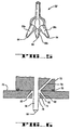
- the above-described embodiment has been designed for substrates 20 having diameters of 8 inches (20 cm). Larger diameter substrates, such as substrates having diameters of 12 inches (30 cm), may call for the use of multiple center nozzles 56a as illustrated in Fig. 5 by the nozzle assembly 56'.
- the deposition thickness variation plot would likely have a three-bump (as in Fig. 3), a four-bump or a five-bump shape.
- the particular shape for the deposition thickness plot would be influenced by the type, number, orientation and spacing of center nozzles 56A and orifices 64.
- oxygen may also be directed into chamber 18 through a number of downwardly and outwardly extending passageways 80 as shown in Fig. 6.
- Each passageway 80 has an orifice 82 where oxygen enters into chamber 18.
- other gases such as argon, may be mixed with one or both of the silane passing through orifice 64 or oxygen passing through annular orifice 76 or orifices 82.
Landscapes
- Chemical & Material Sciences (AREA)
- Engineering & Computer Science (AREA)
- Organic Chemistry (AREA)
- Chemical Kinetics & Catalysis (AREA)
- General Chemical & Material Sciences (AREA)
- Materials Engineering (AREA)
- Mechanical Engineering (AREA)
- Metallurgy (AREA)
- Physics & Mathematics (AREA)
- Inorganic Chemistry (AREA)
- Plasma & Fusion (AREA)
- Analytical Chemistry (AREA)
- Chemical Vapour Deposition (AREA)
- Formation Of Insulating Films (AREA)
- Inorganic Insulating Materials (AREA)
- Insulating Bodies (AREA)
Claims (17)
- Verfahren zum Aufdampfen eines Films auf ein Substrat (20) in einer Aufdampferkammer (2) mit einem Gehäuse mit einem Oberteil (75), wobei das Verfahren die folgenden Schritte aufweist:wobei der Schritt der Zufuhr des dritten Prozessgases in einer solchen Weise ausgeführt wird, dass sich das dritte Prozessgas und das zweite Prozessgas nicht mischen, bis sie sich in der Kammer befinden, und wobei das zweite Prozessgas oder das dritte Prozessgas Silan und das dritte Prozessgas oder das zweite Prozessgas ein Sauerstoff lieferndes Gas respektive aufweist.Zuführen von wenigstens einem ersten Prozessgas in die Kammer (2) an einer Vielzahl von Positionen (34), die ein Substrat (20) in der Kammer (2) umgeben;Zuführen eines zweiten Prozessgases in die Kammer (2) von einer zentralen Düse in einer Position in der Mitte des Oberteils (75), welche Position unter Abstand von und mittig oberhalb des Substrates (20) liegt; undZuführen eines dritten Prozessgases in die Kammer (2) von einer ringförmigen Öffnung, die die zentrale Düse umgibt, in einer Position in der Mitte des Oberteils (75), welche Position unter Abstand von und mittig oberhalb des Substrats (20) liegt,
- Verfahren nach Anspruch 1, worin der Schritt des Zuführens des ersten Prozessgases ausgeführt wird unter Verwendung eines Sauerstoff liefernden Gases, vorzugsweise Sauerstoff, als erstes Prozessgas und eines Fluor liefernden Gases, vorzugsweise Siliciumtetrafluorid, als weiters Prozessgas.
- Verfahren nach Anspruch 1, worin der Schritt des Zuführens des ersten Prozessgases dadurch durchgeführt wird, dass wenigstens Silan als erstes Prozessgas separat von dem Sauerstoff liefernden Gas als ein weiteres Prozessgas zugeführt wird.
- Verfahren nach Anspruch 1, worin der Schritt des Zuführens des zweiten Prozessgases unter Verwendung von wenigstens Silan durchgeführt wird.
- Verfahren nach Anspruch 1, worin die Schritte des Zuführens des ersten und des zweiten Prozessgases unter Verwendung eines Fluor zuführenden Gases und Silan durchgeführt werden.
- Verfahren nach Anspruch 1, worin die Schritte des Zuführens des ersten und des zweiten Prozessgases unter Verwendung von Gasen mit unterschiedlichen Zusammensetzungen durchgeführt werden.
- Verfahren nach Anspruch 1, worin der Schritt des Zuführens des dritten Prozessgases unter Verwendung eines Sauerstoff liefernden Gases, vorzugsweise Sauerstoff, durchgeführt wird.
- Verfahren nach Anspruch 1, worin der Schritt des Zuführens des zweiten Prozessgases unter Verwendung von wenigstens Silan und Silantetrafluorid durchgeführt wird, und worin die Flußrate des Siliciumtetrafluorids und des Silans bei etwa 36 und 44 sccm respektive gewählt werden und eine Gesamtsauerstoffflußrate von weniger als 80 sccm gewählt wird.
- Verfahren nach Anspruch 5, worin eine grafische Darstellung erzeugt wird, in der die Elektrizitätskonstante gegen die Flußrate des Sauerstoff liefernden Gases für jeden Satz der Silan und Fluorid zuführenden Gasflußraten aufgetragen ist, und wobei der gewünschte Satz von Flußraten auf der Basis der minimalen die Elektrizitätskonstanten der grafischen Darstellungen ausgewählt wird.
- Verfahren nach einem der Ansprüche 1 bis 8, worin die drei Zuführungsschritte gleichzeitig ablaufen.
- Aufdampfsystem zur Durchführung eines Verfahrens nach einem der Ansprüche 1 bis 10, umfassend:ein Gehäuse (4) mit einem Oberteil (75), dass eine Kammer (2) definiert;eine Substrathalterung (14) in der Kammer (2);einen ersten Gasverteiler (34) mit einer ersten Mündung (38), die sich in die Kammer anstellen um eine Substrathalterungsoberfläche (16) öffnen;einen zweiten Gasverteiler (56), der eine zentrale Düse (56) aufweist, die an einer Position in der Mitte des Oberteils (75) angeordnet ist, welche Position unter Abstand von und mittig oberhalb des Substrats (20) liegt; undeinen dritten Prozessgasverteiler (70), der eine ringförmige Mündung (76), die die zentrale Düse (56) umgibt, umfasst und an einer Position in der Mitte des Oberteils (75) angeordnet ist, welche Position unter Abstand von und mittig oberhalb des Substrates (20) liegt;worin die ersten, zweiten und dritten Prozessgasverteiler (34, 56, 70) mit ersten, zweiten und dritten Prozessgasquellen (35, 58, 71) verbunden sind, die separat voneinander sind.
- Aufdampfsystem nach Anspruch 11, worin die ersten Mündungen (38) des ersten Gasverteilers (34) unter gleichförmigen Abständen um die Mitte des Substrats (20) herum angeordnet sind.
- Aufdampfsystem nach Anspruch 11 oder 12, worin der erste Gasverteiler (34) einen ersten und einen zweiten Satz von Düsen (34, 34a) aufweist, wobei der erste Satz der Düsen strömungsmäßig von dem zweiten Satz der Düsen isoliert ist.
- Aufdampfsystem nach Anspruch 11, worin die zentrale Düse (56) eine Vielzahl von zweiten Öffnungen (64) aufweist, und der dritte Gasverteiler (70) eine Vielzahl von dritten Mündungen (82) aufweist, die an nach außen versetzten Positionen an der Position in der Mitte des Oberteils (75) angeordnet sind, welche Position unter Abstand von und mittig oberhalb des Substrats (20) liegt.
- Aufdampfsystem nach Anspruch 11, worin das Gehäuse (4) ein Oberteil aufweist, wobei das Oberteil eine Zugangsöffnung (74) durch es hindurch definiert; wobei die zentrale Düse (56) durch die Zugangsmündung (74) hindurch tritt, und wobei der dritte Gasverteiler (70) einen Durchgang (76) aufweist, der in einem Teil einer Strömungsmitteldichtung (78) definiert ist, welches zwischen einem Körper (70) und dem Oberteil (75) eingesetzt ist, und die Zutrittsöffnung (74) umgibt.
- Aufdampfsystem nach Anspruch 15, worin der Durchgang eine Vielzahl von nach außen und unten verlaufenden Wegabschnitten (84) aufweist, die von der Düse (56) unter Abstand sind und zusätzliche Mündungen (82) des dritten Gasverteilers (70) bilden.
- Aufdampfsystem nach Anspruch 11, worin das Gehäuse (4) eine dielektrische Kammer aufweist, wobei die dielektrische Kammer ein Oberteil (75) aufweist, und worin induktive Spulen (8) an dem Gehäuse (4) montiert und mit einem Hochfrequenzgenerator (10, 11) gekoppelt sind.
Applications Claiming Priority (2)
| Application Number | Priority Date | Filing Date | Title |
|---|---|---|---|
| US64761996A | 1996-05-13 | 1996-05-13 | |
| US647619 | 1996-05-13 |
Publications (2)
| Publication Number | Publication Date |
|---|---|
| EP0807694A1 EP0807694A1 (de) | 1997-11-19 |
| EP0807694B1 true EP0807694B1 (de) | 2002-12-11 |
Family
ID=24597681
Family Applications (1)
| Application Number | Title | Priority Date | Filing Date |
|---|---|---|---|
| EP97107815A Expired - Lifetime EP0807694B1 (de) | 1996-05-13 | 1997-05-13 | Aufdampfungskammer und Verfahren zur Herstellung eines Films mit einer niedrigen Dielektrizitätskonstante |
Country Status (6)
| Country | Link |
|---|---|
| EP (1) | EP0807694B1 (de) |
| JP (1) | JP4087923B2 (de) |
| KR (1) | KR100297420B1 (de) |
| AT (1) | ATE229576T1 (de) |
| DE (1) | DE69717711T2 (de) |
| TW (1) | TW343356B (de) |
Families Citing this family (9)
| Publication number | Priority date | Publication date | Assignee | Title |
|---|---|---|---|---|
| US6070551A (en) * | 1996-05-13 | 2000-06-06 | Applied Materials, Inc. | Deposition chamber and method for depositing low dielectric constant films |
| TW416100B (en) * | 1997-07-02 | 2000-12-21 | Applied Materials Inc | Control of oxygen to silane ratio in a seasoning process to improve particle performance in an HDP-CVD system |
| US6486081B1 (en) | 1998-11-13 | 2002-11-26 | Applied Materials, Inc. | Gas distribution system for a CVD processing chamber |
| US6432259B1 (en) * | 1999-12-14 | 2002-08-13 | Applied Materials, Inc. | Plasma reactor cooled ceiling with an array of thermally isolated plasma heated mini-gas distribution plates |
| KR100406173B1 (ko) * | 2000-06-13 | 2003-11-19 | 주식회사 하이닉스반도체 | 촉매 분사 수단을 구비한 히터 블록 |
| CN101351076B (zh) * | 2008-09-16 | 2011-08-17 | 北京北方微电子基地设备工艺研究中心有限责任公司 | 等离子体处理设备 |
| US9512520B2 (en) * | 2011-04-25 | 2016-12-06 | Applied Materials, Inc. | Semiconductor substrate processing system |
| US9499905B2 (en) * | 2011-07-22 | 2016-11-22 | Applied Materials, Inc. | Methods and apparatus for the deposition of materials on a substrate |
| US9284644B2 (en) * | 2014-02-27 | 2016-03-15 | Lam Research Corporation | Apparatus and method for improving wafer uniformity |
Family Cites Families (9)
| Publication number | Priority date | Publication date | Assignee | Title |
|---|---|---|---|---|
| JPS54111771A (en) * | 1978-02-22 | 1979-09-01 | Toshiba Corp | Gas phase reaction unit of semiconductor substrate |
| JPH02126632A (ja) * | 1988-11-05 | 1990-05-15 | Nippon Telegr & Teleph Corp <Ntt> | 化合物半導体結晶層の気相成長方法及びそれに用いる反応管 |
| JPH0521393A (ja) * | 1991-07-11 | 1993-01-29 | Sony Corp | プラズマ処理装置 |
| KR0131439B1 (ko) * | 1992-11-24 | 1998-04-14 | 나카무라 타메아키 | 반도체장치 및 그 제조방법 |
| JPH0729827A (ja) * | 1993-07-13 | 1995-01-31 | Kawasaki Steel Corp | 半導体基板の製造方法および装置 |
| JP2667364B2 (ja) * | 1993-08-16 | 1997-10-27 | キヤノン販売株式会社 | 成膜装置 |
| JPH07161642A (ja) * | 1993-12-03 | 1995-06-23 | Kobe Steel Ltd | プラズマ処理装置 |
| JPH07254592A (ja) * | 1994-03-16 | 1995-10-03 | Fujitsu Ltd | 半導体装置の製造方法 |
| JP3243125B2 (ja) * | 1994-06-27 | 2002-01-07 | 東京エレクトロン株式会社 | 処理装置 |
-
1997
- 1997-05-02 TW TW086105863A patent/TW343356B/zh not_active IP Right Cessation
- 1997-05-07 JP JP15277197A patent/JP4087923B2/ja not_active Expired - Fee Related
- 1997-05-13 AT AT97107815T patent/ATE229576T1/de not_active IP Right Cessation
- 1997-05-13 EP EP97107815A patent/EP0807694B1/de not_active Expired - Lifetime
- 1997-05-13 KR KR1019970018373A patent/KR100297420B1/ko not_active Expired - Lifetime
- 1997-05-13 DE DE69717711T patent/DE69717711T2/de not_active Expired - Fee Related
Also Published As
| Publication number | Publication date |
|---|---|
| TW343356B (en) | 1998-10-21 |
| DE69717711T2 (de) | 2003-09-18 |
| DE69717711D1 (de) | 2003-01-23 |
| KR100297420B1 (ko) | 2001-10-24 |
| KR970077163A (ko) | 1997-12-12 |
| ATE229576T1 (de) | 2002-12-15 |
| EP0807694A1 (de) | 1997-11-19 |
| JPH1064892A (ja) | 1998-03-06 |
| JP4087923B2 (ja) | 2008-05-21 |
Similar Documents
| Publication | Publication Date | Title |
|---|---|---|
| US6070551A (en) | Deposition chamber and method for depositing low dielectric constant films | |
| US7132134B2 (en) | Staggered in-situ deposition and etching of a dielectric layer for HDP CVD | |
| JP4590071B2 (ja) | 基板表面上に誘電体層を形成するための方法及び装置 | |
| US6251187B1 (en) | Gas distribution in deposition chambers | |
| US7294588B2 (en) | In-situ-etch-assisted HDP deposition | |
| US6121161A (en) | Reduction of mobile ion and metal contamination in HDP-CVD chambers using chamber seasoning film depositions | |
| EP1182273B1 (de) | Zyklen der Gaszusammensetzung bei HDP-CVD zur Erhaltung der Lückenfüllung mit hohem Aspektverhältnis | |
| US20080121177A1 (en) | Dual top gas feed through distributor for high density plasma chamber | |
| EP1227172A2 (de) | Verfahren zur Reduzierung von plasmaverusachten Schäden in Plasmaprozessen | |
| US20080121178A1 (en) | Dual top gas feed through distributor for high density plasma chamber | |
| US6521302B1 (en) | Method of reducing plasma-induced damage | |
| EP0807694B1 (de) | Aufdampfungskammer und Verfahren zur Herstellung eines Films mit einer niedrigen Dielektrizitätskonstante | |
| KR20080108067A (ko) | 저온에서의 고밀도 플라즈마 hdp-cvd에 의한 비정질 실리콘막의 증착 | |
| EP1201784A1 (de) | Abscheidung von Siliziumreichem Oxid durch HDP-CVD | |
| KR102046391B1 (ko) | 기판 처리 장치 및 기판 처리 방법 | |
| US6123776A (en) | Gas delivering apparatus for chemical vapor deposition | |
| WO2025117138A1 (en) | Hardware design with independent control to improve wiw uniformity |
Legal Events
| Date | Code | Title | Description |
|---|---|---|---|
| PUAI | Public reference made under article 153(3) epc to a published international application that has entered the european phase |
Free format text: ORIGINAL CODE: 0009012 |
|
| AK | Designated contracting states |
Kind code of ref document: A1 Designated state(s): AT BE CH DE ES FR GB GR IE IT LI NL SE |
|
| RIN1 | Information on inventor provided before grant (corrected) |
Inventor name: COLLINS, ALAN W. Inventor name: ISHIKAWA, TETSUYA Inventor name: REDEKER, FRED C. Inventor name: WANG, YAXIN Inventor name: LI, SHIJIAN |
|
| 17P | Request for examination filed |
Effective date: 19980508 |
|
| 17Q | First examination report despatched |
Effective date: 19990714 |
|
| GRAG | Despatch of communication of intention to grant |
Free format text: ORIGINAL CODE: EPIDOS AGRA |
|
| GRAG | Despatch of communication of intention to grant |
Free format text: ORIGINAL CODE: EPIDOS AGRA |
|
| GRAH | Despatch of communication of intention to grant a patent |
Free format text: ORIGINAL CODE: EPIDOS IGRA |
|
| GRAH | Despatch of communication of intention to grant a patent |
Free format text: ORIGINAL CODE: EPIDOS IGRA |
|
| GRAA | (expected) grant |
Free format text: ORIGINAL CODE: 0009210 |
|
| AK | Designated contracting states |
Kind code of ref document: B1 Designated state(s): AT BE CH DE ES FR GB GR IE IT LI NL SE |
|
| PG25 | Lapsed in a contracting state [announced via postgrant information from national office to epo] |
Ref country code: LI Free format text: LAPSE BECAUSE OF FAILURE TO SUBMIT A TRANSLATION OF THE DESCRIPTION OR TO PAY THE FEE WITHIN THE PRESCRIBED TIME-LIMIT Effective date: 20021211 Ref country code: IT Free format text: LAPSE BECAUSE OF FAILURE TO SUBMIT A TRANSLATION OF THE DESCRIPTION OR TO PAY THE FEE WITHIN THE PRESCRIBED TIME-LIMIT;WARNING: LAPSES OF ITALIAN PATENTS WITH EFFECTIVE DATE BEFORE 2007 MAY HAVE OCCURRED AT ANY TIME BEFORE 2007. THE CORRECT EFFECTIVE DATE MAY BE DIFFERENT FROM THE ONE RECORDED. Effective date: 20021211 Ref country code: GR Free format text: LAPSE BECAUSE OF FAILURE TO SUBMIT A TRANSLATION OF THE DESCRIPTION OR TO PAY THE FEE WITHIN THE PRESCRIBED TIME-LIMIT Effective date: 20021211 Ref country code: CH Free format text: LAPSE BECAUSE OF FAILURE TO SUBMIT A TRANSLATION OF THE DESCRIPTION OR TO PAY THE FEE WITHIN THE PRESCRIBED TIME-LIMIT Effective date: 20021211 Ref country code: BE Free format text: LAPSE BECAUSE OF FAILURE TO SUBMIT A TRANSLATION OF THE DESCRIPTION OR TO PAY THE FEE WITHIN THE PRESCRIBED TIME-LIMIT Effective date: 20021211 Ref country code: AT Free format text: LAPSE BECAUSE OF FAILURE TO SUBMIT A TRANSLATION OF THE DESCRIPTION OR TO PAY THE FEE WITHIN THE PRESCRIBED TIME-LIMIT Effective date: 20021211 |
|
| REF | Corresponds to: |
Ref document number: 229576 Country of ref document: AT Date of ref document: 20021215 Kind code of ref document: T |
|
| REG | Reference to a national code |
Ref country code: GB Ref legal event code: FG4D |
|
| REG | Reference to a national code |
Ref country code: CH Ref legal event code: EP |
|
| REG | Reference to a national code |
Ref country code: IE Ref legal event code: FG4D |
|
| REF | Corresponds to: |
Ref document number: 69717711 Country of ref document: DE Date of ref document: 20030123 |
|
| PG25 | Lapsed in a contracting state [announced via postgrant information from national office to epo] |
Ref country code: SE Free format text: LAPSE BECAUSE OF FAILURE TO SUBMIT A TRANSLATION OF THE DESCRIPTION OR TO PAY THE FEE WITHIN THE PRESCRIBED TIME-LIMIT Effective date: 20030311 |
|
| PG25 | Lapsed in a contracting state [announced via postgrant information from national office to epo] |
Ref country code: IE Free format text: LAPSE BECAUSE OF NON-PAYMENT OF DUE FEES Effective date: 20030513 |
|
| PG25 | Lapsed in a contracting state [announced via postgrant information from national office to epo] |
Ref country code: ES Free format text: LAPSE BECAUSE OF FAILURE TO SUBMIT A TRANSLATION OF THE DESCRIPTION OR TO PAY THE FEE WITHIN THE PRESCRIBED TIME-LIMIT Effective date: 20030627 |
|
| REG | Reference to a national code |
Ref country code: CH Ref legal event code: PL |
|
| ET | Fr: translation filed | ||
| PLBE | No opposition filed within time limit |
Free format text: ORIGINAL CODE: 0009261 |
|
| STAA | Information on the status of an ep patent application or granted ep patent |
Free format text: STATUS: NO OPPOSITION FILED WITHIN TIME LIMIT |
|
| 26N | No opposition filed |
Effective date: 20030912 |
|
| REG | Reference to a national code |
Ref country code: IE Ref legal event code: MM4A |
|
| PGFP | Annual fee paid to national office [announced via postgrant information from national office to epo] |
Ref country code: FR Payment date: 20050517 Year of fee payment: 9 |
|
| PGFP | Annual fee paid to national office [announced via postgrant information from national office to epo] |
Ref country code: GB Payment date: 20060406 Year of fee payment: 10 |
|
| GBPC | Gb: european patent ceased through non-payment of renewal fee |
Effective date: 20070513 |
|
| REG | Reference to a national code |
Ref country code: FR Ref legal event code: ST Effective date: 20080131 |
|
| PG25 | Lapsed in a contracting state [announced via postgrant information from national office to epo] |
Ref country code: GB Free format text: LAPSE BECAUSE OF NON-PAYMENT OF DUE FEES Effective date: 20070513 |
|
| PG25 | Lapsed in a contracting state [announced via postgrant information from national office to epo] |
Ref country code: FR Free format text: LAPSE BECAUSE OF NON-PAYMENT OF DUE FEES Effective date: 20070531 |
|
| PGFP | Annual fee paid to national office [announced via postgrant information from national office to epo] |
Ref country code: DE Payment date: 20080530 Year of fee payment: 12 |
|
| PG25 | Lapsed in a contracting state [announced via postgrant information from national office to epo] |
Ref country code: FR Free format text: LAPSE BECAUSE OF NON-PAYMENT OF DUE FEES Effective date: 20060531 |
|
| PGFP | Annual fee paid to national office [announced via postgrant information from national office to epo] |
Ref country code: NL Payment date: 20080410 Year of fee payment: 12 |
|
| NLV4 | Nl: lapsed or anulled due to non-payment of the annual fee |
Effective date: 20091201 |
|
| PG25 | Lapsed in a contracting state [announced via postgrant information from national office to epo] |
Ref country code: NL Free format text: LAPSE BECAUSE OF NON-PAYMENT OF DUE FEES Effective date: 20091201 |
|
| PG25 | Lapsed in a contracting state [announced via postgrant information from national office to epo] |
Ref country code: DE Free format text: LAPSE BECAUSE OF NON-PAYMENT OF DUE FEES Effective date: 20091201 |