EP0804019B1 - Schaltung zur Begrenzung des Strahlstroms einer Bildröhre - Google Patents
Schaltung zur Begrenzung des Strahlstroms einer Bildröhre Download PDFInfo
- Publication number
- EP0804019B1 EP0804019B1 EP97106150A EP97106150A EP0804019B1 EP 0804019 B1 EP0804019 B1 EP 0804019B1 EP 97106150 A EP97106150 A EP 97106150A EP 97106150 A EP97106150 A EP 97106150A EP 0804019 B1 EP0804019 B1 EP 0804019B1
- Authority
- EP
- European Patent Office
- Prior art keywords
- beam current
- temperature
- circuit
- transformer
- temperature sensor
- Prior art date
- Legal status (The legal status is an assumption and is not a legal conclusion. Google has not performed a legal analysis and makes no representation as to the accuracy of the status listed.)
- Expired - Lifetime
Links
- 230000001419 dependent effect Effects 0.000 claims description 14
- 238000004804 winding Methods 0.000 claims description 13
- 230000007774 longterm Effects 0.000 claims description 4
- 229910000859 α-Fe Inorganic materials 0.000 description 9
- 239000000243 solution Substances 0.000 description 5
- 239000004020 conductor Substances 0.000 description 3
- 239000003990 capacitor Substances 0.000 description 2
- 238000001816 cooling Methods 0.000 description 2
- 230000007423 decrease Effects 0.000 description 2
- 238000010586 diagram Methods 0.000 description 2
- 238000012986 modification Methods 0.000 description 2
- 230000004048 modification Effects 0.000 description 2
- 230000001105 regulatory effect Effects 0.000 description 2
- 150000001875 compounds Chemical class 0.000 description 1
- 230000006378 damage Effects 0.000 description 1
- 238000011161 development Methods 0.000 description 1
- 230000018109 developmental process Effects 0.000 description 1
- 238000009413 insulation Methods 0.000 description 1
- 238000012544 monitoring process Methods 0.000 description 1
- 238000013021 overheating Methods 0.000 description 1
- 238000004382 potting Methods 0.000 description 1
- 238000012545 processing Methods 0.000 description 1
- 230000000630 rising effect Effects 0.000 description 1
Images
Classifications
-
- H—ELECTRICITY
- H04—ELECTRIC COMMUNICATION TECHNIQUE
- H04N—PICTORIAL COMMUNICATION, e.g. TELEVISION
- H04N5/00—Details of television systems
- H04N5/66—Transforming electric information into light information
- H04N5/68—Circuit details for cathode-ray display tubes
-
- H—ELECTRICITY
- H04—ELECTRIC COMMUNICATION TECHNIQUE
- H04N—PICTORIAL COMMUNICATION, e.g. TELEVISION
- H04N3/00—Scanning details of television systems; Combination thereof with generation of supply voltages
- H04N3/10—Scanning details of television systems; Combination thereof with generation of supply voltages by means not exclusively optical-mechanical
- H04N3/16—Scanning details of television systems; Combination thereof with generation of supply voltages by means not exclusively optical-mechanical by deflecting electron beam in cathode-ray tube, e.g. scanning corrections
- H04N3/20—Prevention of damage to cathode-ray tubes in the event of failure of scanning
Definitions
- the invention relates to a circuit for limiting the Beam current of a picture tube in a television receiver according to the Preamble of claim 1.
- limiter function For circuits to limit the beam current is in generally only a limiter function is effective. To briefly White areas of the image appearing with sufficient brightness to represent, the limit value is set so that it lies above the beam current with which the picture tube in Continuous operation may be loaded without being damaged. in the The long-term average is normal operation with moving images (long term average) always below this maximum limit of Strahstroms, since there are also dark scenes in between the limitation is not effective. A continuous operation with active Beam current limitation is theoretically possible.
- the invention has for its object a higher Beam current for white areas of the image and thus a brighter image enable without this in the extreme mentioned Load case of the high-voltage transformer is at risk.
- This object is achieved by the invention specified in claim 1 solved.
- Advantageous developments of the invention are in the Subclaims specified.
- the invention thus consists in the transformer being one Contains temperature sensor that is above a certain one Temperature on the control circuit for the beam current in the sense reducing the jet current.
- the temperature sensor is in the form of a temperature dependent resistor together with the bobbin, the windings and the Rectifier diodes cast in a plastic body.
- the invention is based on the following findings and Considerations.
- the extreme load case mentioned can be in do not rule out practice and must be taken into account when Beam current limiting circuit must be taken into account.
- a Danger or destruction of the transformer is the only thing possible due to an increased temperature of the transformer. Therefore according to the invention, the temperature of the high-voltage transformer supervised. If the temperature of the transformer and thus also that of the rectifier diodes a certain value exceeds the beam current in the sense of a control loop so regulated back that even during the extreme In case of load, a permissible temperature at the transformer of e.g. 100 °.
- the solution according to the invention has several advantages. There one imminent danger to the high voltage transformer in an extreme load due to temperature monitoring recognized and caught, can be used for normal operation with moving pictures a higher beam current allowed and thus a brighter picture can be obtained without using the transformer there is a danger.
- the high voltage transformer remains the temperature control is protected in all cases. In particular the rectifier diodes cannot reach an unacceptably high temperature reach and the core of the transformer does not saturate reach. If necessary, the high voltage transformer be built smaller and cheaper.
- the invention Measure requires only a few components, e.g. one temperature dependent resistance, an ohmic resistance and a diode.
- the device itself becomes practically indestructible, itself if in extreme cases at + 40 ° C ambient temperature below having bad cooling conditions over a variety of hours is operated in a completely white image.
- the brightness is reduced in the extreme case mentioned.
- the but is practically no disadvantage, because with the extreme mentioned Load case anyway there is no normal picture, the change the brightness is noticeably slow with suitable dimensioning and this is usually the case with a specific device occurs rarely or never.
- the circuit controlled by the temperature sensor is preferably dimensioned so that they have a long-term beam current behavior due to moving pictures with normal average brightness does not respond.
- the temperature sensor is preferably by a temperature dependent Resistor, a so-called NTC or PTC resistor, educated. Such resistors are commercially available and inexpensive. The ends of the resistor are two Terminals of the transformer connected. It has shown that with this solution the temperature of the resistor with sufficient accuracy and time constant of the temperature the Rectifier diodes follow. The temperature at that So temperature dependent resistance is a real measure of that Temperature of the rectifier diodes.
- the temperature dependent resistance close to the core of the Transformer. It is also achieved that the Resistance temperature sufficiently accurate and fast Temperature of the rectifier diodes follows. This arrangement has the advantage that the cores are at ground potential, ie is not in the high voltage range and therefore none Insulation problems with the temperature-dependent resistor arise.
- the resistance can also be between the core and one of the Transformer carrying printed circuit board. there the arrangement is such that the heat from the core as good as possible on the resistance, but as little as possible on the printed circuit board and the conductor tracks contained on it is transmitted.
- the temperature-dependent resistance can also be in a recess like a notch on a surface of the core. Thereby the thermal contact between the core and the resistor can still can be improved by using the core with the resistance about 180 ° whose circumference is in direct contact.
- the temperature dependent resistance can also be in a Plastic body embedded between the core and the PCB is bordered.
- the temperature sensor preferably forms part of a network, that via a threshold circuit with a beam current influencing control terminal of a picture tube drive circuit connected is.
- the Series connection of the temperature-dependent resistor and one further ohmic resistance between an operating voltage and earth, and the center of the series connection is over one Diode with the control terminal influencing the beam current connected.
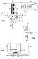
- Fig. 1 shows the high voltage transformer Tr, the High voltage UH for the picture tube 1 of a television receiver supplies.
- the primary winding 2 of the transformer Tr is connected to the Operating voltage + UB and one through the switching voltage 3 periodically actuated switching transistor 4 connected to earth.
- the High-voltage winding 5 is a diode split winding with several High voltage rectifier diodes 6 are formed.
- the Control signals R, G, B are the picture tube 1 via the video power amplifier 7 supplied and control the jet currents is in the Picture tube 1.
- Resistors R3 and R4 form one Voltage divider with the filter capacitor C1.
- the resistor R3 is connected to the operating voltage + U2 and acts as Power source.
- the one flowing through resistor R4 Beam current is zero, only a current of + U2 flows over the Resistor R3 into resistor R4 and generates a at point b Voltage U4.
- the high-voltage winding 5 takes over a part of current through resistor R3, thereby reducing the Voltage across resistor R3 to lower or even negative values.
- the voltage U4 is used as a manipulated variable for the Beam current limitation to the control terminal a of the video amplifier 7 created. The circuit described so far is known.
- the series connection is now made of the PTC resistor R2 and the resistor R1 between the operating voltage + U1 and Earth and the diode D1 provided.
- the resistance R2 is narrow to the ferrite core 8 of the transformer Tr.
- the voltage divider from the resistors R1, R2 thus supplies a voltage that of the respective temperature of the ferrite core 8 is dependent.
- the voltage U3 is greater than the voltage U4, so that point c is blocked by diode D1 from point b is decoupled. If the temperature of the transformer Tr, thus also the temperature of the ferrite core 8 and the resistor R2 increases, R2 becomes low-resistance, so that the voltage U3 drops.
- Fig. 2 shows a modification of the circuit of Fig. 1.
- the resistor R1 instead of the PTC resistor R2 is the resistor R1 as an NTC resistor formed and arranged on the ferrite core 8.
- the Operation is practically the same as in Fig. 1. If the Temperature of the ferrite core 8 increases, the resistance R1 high impedance, so that as in Fig. 1, the voltage U3 at point c decreases and finally the above a certain temperature Diode D1 becomes conductive and triggers the beam current limitation.
- FIG. 3 shows the arrangement of the resistor R1 according to FIG. 2 or R1 on FIG. 2 on the ferrite core 8.
- the resistor R1 or R2 is embedded in a plastic body 9, which between the Lower edge of the ferrite core 8 and the printed circuit board 10 lies and is held by the bracket 11.
- the housing of the High voltage transformer Tr is symbolic by the Plastic body 12 indicated.
- the temperature-dependent resistor R1 or R2 is included poured into the plastic body 12, in which the Coil former, the primary winding 2 arranged thereon, the Secondary winding 6 and, if necessary, additional windings and the High-voltage rectifier diodes are cast in.
- the ends of the Resistor R1 or R2 are with two additional connection pins 20 connected in corresponding conductor tracks on the printed circuit board 10 engage and the circuit of the Resistance R1 or R2 according to FIG. 1 or 2 cause.
- the Plastic body 12, which is the actual housing of the Transformers still contains a variety of Connection pins 21 for the primary winding the high voltage winding and, if necessary, further additional windings.
- the connection pins 21 are also with corresponding conductor tracks on the Bottom of the circuit board 10 connected.
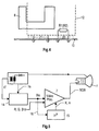
- FIG. 5 shows a simplified block diagram of the picture tube control circuit of the television receiver that the invention 1 to 4 includes the solution.
- the circuit 14 supplies the manipulated variable Bis for the Beam current limitation to the video processor 7, the Control signals R, G, B to the picture tube 1 delivers.
- the signals R, G, B are the video processor 7 from a known Signal processing circuit supplied.
- the microprocessor 15 delivers control signals for the contrast K and the brightness H. the processor 7.
- the dotted line 16 can optionally used additionally because the control loop can be closed via the microprocessor 15. This is also able to adjust the beam current by Control contrast and brightness like this in general takes place within the video processor 7.
Landscapes
- Engineering & Computer Science (AREA)
- Multimedia (AREA)
- Signal Processing (AREA)
- Details Of Television Scanning (AREA)
- Transforming Electric Information Into Light Information (AREA)
- Processing Of Color Television Signals (AREA)
Applications Claiming Priority (2)
| Application Number | Priority Date | Filing Date | Title |
|---|---|---|---|
| DE19616272 | 1996-04-24 | ||
| DE19616272A DE19616272A1 (de) | 1996-04-24 | 1996-04-24 | Schaltung zur Begrenzung des Strahlstroms einer Bildröhre |
Publications (3)
| Publication Number | Publication Date |
|---|---|
| EP0804019A2 EP0804019A2 (de) | 1997-10-29 |
| EP0804019A3 EP0804019A3 (de) | 1997-11-19 |
| EP0804019B1 true EP0804019B1 (de) | 2002-07-24 |
Family
ID=7792246
Family Applications (1)
| Application Number | Title | Priority Date | Filing Date |
|---|---|---|---|
| EP97106150A Expired - Lifetime EP0804019B1 (de) | 1996-04-24 | 1997-04-15 | Schaltung zur Begrenzung des Strahlstroms einer Bildröhre |
Country Status (5)
| Country | Link |
|---|---|
| US (1) | US6040664A (enExample) |
| EP (1) | EP0804019B1 (enExample) |
| JP (1) | JPH1070693A (enExample) |
| CN (1) | CN1160951C (enExample) |
| DE (2) | DE19616272A1 (enExample) |
Families Citing this family (4)
| Publication number | Priority date | Publication date | Assignee | Title |
|---|---|---|---|---|
| JP3833843B2 (ja) * | 1999-04-06 | 2006-10-18 | Necディスプレイソリューションズ株式会社 | 画像補正方法及び画像補正装置並びに陰極線管ディスプレイ装置 |
| US6636265B1 (en) * | 2000-01-21 | 2003-10-21 | Thomson Licensing S.A. | Focus flutter prevention in TV receivers and monitors |
| KR20040068680A (ko) * | 2003-01-27 | 2004-08-02 | 삼성전자주식회사 | 고압 변압기 |
| KR20080079449A (ko) | 2007-02-27 | 2008-09-01 | 삼성전자주식회사 | 영상 디스플레이장치 및 영상 디스플레이장치에서의 과전류제어방법 |
Family Cites Families (6)
| Publication number | Priority date | Publication date | Assignee | Title |
|---|---|---|---|---|
| JPS5630985B2 (enExample) * | 1973-10-16 | 1981-07-18 | ||
| US4042858A (en) * | 1976-07-08 | 1977-08-16 | Gte Sylvania Incorporated | Television receiver protection circuit |
| US4126816A (en) * | 1977-05-13 | 1978-11-21 | Rca Corporation | High voltage protection circuit |
| US4645988A (en) * | 1985-12-11 | 1987-02-24 | Zenith Electronics Corporation | Temperature compensated drive circuit for CRT G2 grid |
| US4945414A (en) * | 1988-05-12 | 1990-07-31 | Rca Licensing Corporation | Compensator for temperature-induced black level drift for use in a television receiver |
| JPH04134973A (ja) * | 1990-09-26 | 1992-05-08 | Mitsubishi Electric Corp | フライバックトランスの発煙防止装置 |
-
1996
- 1996-04-24 DE DE19616272A patent/DE19616272A1/de not_active Withdrawn
-
1997
- 1997-03-24 CN CNB971030855A patent/CN1160951C/zh not_active Expired - Fee Related
- 1997-04-15 EP EP97106150A patent/EP0804019B1/de not_active Expired - Lifetime
- 1997-04-15 DE DE59707761T patent/DE59707761D1/de not_active Expired - Fee Related
- 1997-04-22 JP JP9103740A patent/JPH1070693A/ja active Pending
-
1998
- 1998-02-25 US US08/999,879 patent/US6040664A/en not_active Expired - Fee Related
Also Published As
| Publication number | Publication date |
|---|---|
| CN1171695A (zh) | 1998-01-28 |
| DE19616272A1 (de) | 1997-10-30 |
| DE59707761D1 (de) | 2002-08-29 |
| US6040664A (en) | 2000-03-21 |
| EP0804019A3 (de) | 1997-11-19 |
| CN1160951C (zh) | 2004-08-04 |
| EP0804019A2 (de) | 1997-10-29 |
| JPH1070693A (ja) | 1998-03-10 |
Similar Documents
| Publication | Publication Date | Title |
|---|---|---|
| DE2843705C2 (enExample) | ||
| DE3422135C2 (de) | Monolithisch integrierbarer Spannungsstabilisator mit breitem Anwendungsbereich für den Einsatz in Kraftfahrzeugen | |
| DE69902891T2 (de) | Referenzspannungsgenerator mit Überwachungs- und Anlaufschaltung | |
| EP0804019B1 (de) | Schaltung zur Begrenzung des Strahlstroms einer Bildröhre | |
| DE2834678C2 (de) | Schaltungsanordnung mit Kurzschlußschutz | |
| DE69838973T2 (de) | Schwachstromüberwachung durch "low-side" getriebenen DMOS mittels Modulierung seines inneren Widerstands | |
| DE2700274A1 (de) | Stromversorgungseinrichtung fuer bildverstaerker | |
| DE1943239A1 (de) | Temperaturstabile Schwellwertschaltungsanordnung | |
| DE69407723T2 (de) | Schaltungsanordnung zum Einspeisen von Gleichstrom in eine Wicklung | |
| DE3000595C2 (enExample) | ||
| EP0018598A1 (de) | Schaltungsanordnung zur Begrenzung des Schaltstroms in einem aus einem Durchflussstromwandler, einem Schalthalbleiter, einer Schutzinduktivität und einer Überstromabschaltung in Serienschaltung gebildeten Stromkreis | |
| DE2840115A1 (de) | Schaltanordnung fuer eine elektromagnetische fokussier-bildaufnahmeroehre | |
| DE2930216C2 (enExample) | ||
| DE3891380C2 (de) | Verstärker mit vier Transistoren, die in einer Brückenschaltung miteinander verbunden sind | |
| DE2702536A1 (de) | Ab-verstaerker mit konstantem stromverbrauch | |
| DE2645706C2 (de) | Horizontalablenkschaltung für eine Fernsehkamera | |
| DE2062605C3 (de) | Vertikalablenkschaltung | |
| DE2429794A1 (de) | Signalbegrenzerschaltung | |
| DE69113860T2 (de) | Schaltungsanordnung zur Regelung des Leitungsstroms in einem Telefonapparat. | |
| DE2733006B2 (de) | Temperaturwächter | |
| DE3111659A1 (de) | Annaeherungsschalter mit umschalterausgang | |
| DE3878945T2 (de) | Vorrichtung zur speisung elektrischer energie fuer ein kabel und seine anwendung. | |
| DE2513804A1 (de) | Spannungsspeichereinrichtung | |
| DE1911959A1 (de) | Triggerschaltung | |
| DE19833968A1 (de) | Integrierte Reglervorrichtung |
Legal Events
| Date | Code | Title | Description |
|---|---|---|---|
| PUAI | Public reference made under article 153(3) epc to a published international application that has entered the european phase |
Free format text: ORIGINAL CODE: 0009012 |
|
| PUAL | Search report despatched |
Free format text: ORIGINAL CODE: 0009013 |
|
| AK | Designated contracting states |
Kind code of ref document: A2 Designated state(s): DE FR GB IT |
|
| AK | Designated contracting states |
Kind code of ref document: A3 Designated state(s): DE FR GB IT |
|
| 17P | Request for examination filed |
Effective date: 19980505 |
|
| 17Q | First examination report despatched |
Effective date: 20000120 |
|
| GRAG | Despatch of communication of intention to grant |
Free format text: ORIGINAL CODE: EPIDOS AGRA |
|
| GRAG | Despatch of communication of intention to grant |
Free format text: ORIGINAL CODE: EPIDOS AGRA |
|
| GRAH | Despatch of communication of intention to grant a patent |
Free format text: ORIGINAL CODE: EPIDOS IGRA |
|
| GRAH | Despatch of communication of intention to grant a patent |
Free format text: ORIGINAL CODE: EPIDOS IGRA |
|
| GRAA | (expected) grant |
Free format text: ORIGINAL CODE: 0009210 |
|
| AK | Designated contracting states |
Kind code of ref document: B1 Designated state(s): DE FR GB IT |
|
| REG | Reference to a national code |
Ref country code: GB Ref legal event code: FG4D Free format text: NOT ENGLISH |
|
| GBT | Gb: translation of ep patent filed (gb section 77(6)(a)/1977) |
Effective date: 20020725 |
|
| REG | Reference to a national code |
Ref country code: GB Ref legal event code: 746 Effective date: 20020807 |
|
| REF | Corresponds to: |
Ref document number: 59707761 Country of ref document: DE Date of ref document: 20020829 |
|
| ET | Fr: translation filed | ||
| REG | Reference to a national code |
Ref country code: FR Ref legal event code: D6 |
|
| PLBE | No opposition filed within time limit |
Free format text: ORIGINAL CODE: 0009261 |
|
| STAA | Information on the status of an ep patent application or granted ep patent |
Free format text: STATUS: NO OPPOSITION FILED WITHIN TIME LIMIT |
|
| 26N | No opposition filed |
Effective date: 20030425 |
|
| PGFP | Annual fee paid to national office [announced via postgrant information from national office to epo] |
Ref country code: GB Payment date: 20080326 Year of fee payment: 12 |
|
| PGFP | Annual fee paid to national office [announced via postgrant information from national office to epo] |
Ref country code: IT Payment date: 20090427 Year of fee payment: 13 Ref country code: DE Payment date: 20090423 Year of fee payment: 13 |
|
| GBPC | Gb: european patent ceased through non-payment of renewal fee |
Effective date: 20090415 |
|
| REG | Reference to a national code |
Ref country code: FR Ref legal event code: ST Effective date: 20091231 |
|
| PG25 | Lapsed in a contracting state [announced via postgrant information from national office to epo] |
Ref country code: GB Free format text: LAPSE BECAUSE OF NON-PAYMENT OF DUE FEES Effective date: 20090415 Ref country code: FR Free format text: LAPSE BECAUSE OF NON-PAYMENT OF DUE FEES Effective date: 20091222 |
|
| PGFP | Annual fee paid to national office [announced via postgrant information from national office to epo] |
Ref country code: FR Payment date: 20080425 Year of fee payment: 12 |
|
| PG25 | Lapsed in a contracting state [announced via postgrant information from national office to epo] |
Ref country code: DE Free format text: LAPSE BECAUSE OF NON-PAYMENT OF DUE FEES Effective date: 20101103 |
|
| PG25 | Lapsed in a contracting state [announced via postgrant information from national office to epo] |
Ref country code: IT Free format text: LAPSE BECAUSE OF NON-PAYMENT OF DUE FEES Effective date: 20100415 |