EP0803327A2 - Dispositif et procédé pour le profilage de patins de polissage - Google Patents
Dispositif et procédé pour le profilage de patins de polissage Download PDFInfo
- Publication number
- EP0803327A2 EP0803327A2 EP97302420A EP97302420A EP0803327A2 EP 0803327 A2 EP0803327 A2 EP 0803327A2 EP 97302420 A EP97302420 A EP 97302420A EP 97302420 A EP97302420 A EP 97302420A EP 0803327 A2 EP0803327 A2 EP 0803327A2
- Authority
- EP
- European Patent Office
- Prior art keywords
- polishing
- pad
- shaping
- fixture
- shaping tool
- Prior art date
- Legal status (The legal status is an assumption and is not a legal conclusion. Google has not performed a legal analysis and makes no representation as to the accuracy of the status listed.)
- Withdrawn
Links
Images

Classifications
-
- B—PERFORMING OPERATIONS; TRANSPORTING
- B24—GRINDING; POLISHING
- B24B—MACHINES, DEVICES, OR PROCESSES FOR GRINDING OR POLISHING; DRESSING OR CONDITIONING OF ABRADING SURFACES; FEEDING OF GRINDING, POLISHING, OR LAPPING AGENTS
- B24B53/00—Devices or means for dressing or conditioning abrasive surfaces
- B24B53/017—Devices or means for dressing, cleaning or otherwise conditioning lapping tools
-
- H—ELECTRICITY
- H10—SEMICONDUCTOR DEVICES; ELECTRIC SOLID-STATE DEVICES NOT OTHERWISE PROVIDED FOR
- H10P—GENERIC PROCESSES OR APPARATUS FOR THE MANUFACTURE OR TREATMENT OF DEVICES COVERED BY CLASS H10
- H10P52/00—Grinding, lapping or polishing of wafers, substrates or parts of devices
Definitions
- This invention relates generally to maintenance of polishing pads and more particularly to shaping a polishing pad to maintain flatness of a semiconductor wafer.
- the final step in a conventional semiconductor wafer shaping process is a polishing step to produce a highly reflective, damage-free and flat surface on one face of the semiconductor wafer.
- Polishing usually includes both shaping, which is accomplished by one or more rough polishing steps, and final smoothing, which is accomplished by a finish polishing step. Typically, 95-98% of the stock removal occurs in the rough polishing step(s) which largely determines the final wafer flatness.
- Semiconductor wafers must be polished particularly flat in preparation for printing circuits on the wafers by an electron beam-lithographic or photolithographic process. Flatness of the wafer surface on which circuits are to be printed is critical in order to maintain resolution of the lines, which can be as thin as 1 micron or less.
- TTV Total Thickness Variation measurement
- STIR Site Total Indicated Reading
- TTV is the difference between the maximum and minimum thicknesses of the wafer and represents an upper limit to wafer flatness.
- STIR is the sum of the maximum positive and negative deviations of the surface in a small area of the wafer from a reference plane which is parallel to the back surface of the wafer and intersects the front surface at the center of the local site.
- Total thickness variation in the wafer is a critical indicator of the quality of the polish of the wafer.
- a polished semiconductor wafer will have a TTV of less than one micron and a STIR of less than one-half micron for any 20mm X 20mm local site.
- Polishing of the semiconductor wafer is accomplished by a mechanochemical process in which a rotating polishing pad rubs a polishing slurry against the wafer.
- a surface of the wafer is bonded with wax flat against a polishing block.
- the wafer and polishing block unit is then held with force by a polishing arm against a polishing surface (i.e., that portion of the upper surface area of the pad which contacts and polishes the wafer) of the rotating polishing pad.
- the polishing arm may also move the wafers across the polishing pad in an oscillatory fashion as the pad rotates underneath them.
- the rigid polishing block provides a reference plane with respect to which the polishing surface of the wafer is shaped by polishing to be an essentially parallel, flat plane. As a result, the opposing surfaces of the wafer are parallel to each other.
- a typical rough polisher pad is made of polyester fibers impregnated with polyurethane resin.
- the pad structure remains sufficiently porous after impregnation of the fibers with resin to carry the slurry under the wafer.
- the pad may have a central opening, such that the pad has an annular shape.
- the slurry is typically comprised of a colloidal dispersion of ultrafine particles in an aqueous medium together with additives which stabilize the colloid. Other additives may also be used to increase chemical reactivity of the slurry so as to increase polishing rates.
- the polishing pad must remain substantially flat in order to produce a wafer having a flat polished surface.
- the heat and pressure on the polishing pad causes a central annular region of the pad between its annular inner and outer edge margins to become compressed so that it is thinner than the inner and outer edge margins.
- the cross sectional profile of the polishing surface of the pad becomes concave.
- Wafers polished by a pad of concave cross section are shaped with polished surfaces which are more convex than flat. Accordingly, the polishing pad must be re-shaped to lower the inner and outer edge margins of the pad to the level of the central region by abrading away the inner and outer edge margins.
- Pad shaping is currently accomplished manually using hand held abrading blocks having a working area much smaller than the polishing surface of the polishing pad.
- the block is not capable of engaging the polishing surface across its full radial width at any one time.
- Pad shaping is carried out by moving the block across the pad so that some of the pad underneath the block is abraded away. For instance, the block may be moved along parallel chords across the polishing pad to reduce the concavity of the pad. Occasionally when the pad is too convex in cross section (e.g., when it is a new pad) the block may be moved along diametrical lines passing through the center of the pad to reduce the convexity of the pad.
- the existing pad shaping method results in uneven shaping of the pad so that, for example, the radially inner area of the polishing surface of the pad produces a convex wafer while the radially outer area produces a concave wafer.
- the pad will be shaped in the same way every time it is abraded using the existing method, which relies entirely on human judgment.
- Another problem arises when the polishing surface is less than the entire upper surface area of the pad.
- the unused areas of the pad tend to be very high relative to the polishing surface and require extensive abrading to bring level with the polishing surface of the pad. It is very difficult to bring down the unused areas without over-abrading the areas of the polishing surface adjacent to the unused areas of the pad.
- Apparatus of the present invention is used for shaping a polishing pad mounted for rotation about a center of rotation on a polishing machine for polishing and shaping objects.
- the polishing pad has a polishing surface defined by a radially inner and a radially outer boundary and having a predetermined radial width.
- the polishing surface has a cross sectional profile between its radially inner and outer boundaries.
- the apparatus comprises a pad shaping tool having a center and a pad shaping surface engageable with the polishing surface of the polishing pad for shaping the polishing surface to change the cross sectional profile of the polishing surface from a curved shape to a more flat shape.
- a fixture is constructed for holding the pad shaping tool free of fixed connection thereto in a position in which the shaping surface of the pad shaping tool engages the polishing pad for shaping the pad as the pad rotates relative to the fixture and pad shaping tool.
- the fixture constrains the pad shaping tool from rotation about the center of rotation of the polishing pad and constrains the center of the pad shaping tool from substantial radial movement relative to the center of the polishing pad.
- a method for polishing semiconductor wafers, using a wafer polishing machine having a rotating polishing pad including a polishing surface as previously defined generally comprises the step of polishing at least one face of each of a first plurality of semiconductor wafers.
- the cross sectional profile of the polishing surface is monitored to determine whether the profile of the polishing surface becomes more curved in shape than permitted by a process tolerance amount. If the determined shape of the profile of the polishing surface is more curved than the process tolerance amount, the polishing pad is shaped by placing a pad shaping tool in a fixture such that a pad shaping surface of the tool engages the polishing surface of the polishing pad across the entire radial width of the polishing surface.
- the polishing pad is rotated while the pad shaping tool is constrained by the fixture from rotation about the center of rotation of the polishing pad whereby the pad shaping tool shapes the polishing surface. Thereafter, at least one face of each of a second plurality of semiconductor wafers is polished.
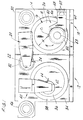
- the rough polishing machine 10 includes a table 14 which supports a polishing pad (generally indicated at 16) mounted on a turntable, which is not shown in the drawings because it is covered by the polishing pad.
- the turntable is capable of rotating the polishing pad 16 with respect to the table 14 about a center of rotation C 1 .
- a drip pan 18 underneath the pad 16 catches polishing slurry which drips off of the polishing pad.
- a polishing arm generally indicated at 20, includes a chuck 22 for holding a polishing block and wafer mounted thereon (not shown) for polishing one face of the wafer on the polishing pad 16.
- a tube 24 mounted on the polishing arm 20 is capable of delivering a polishing slurry to the polishing pad 16.
- the polishing pad 16 is generally annular in shape and, in the preferred embodiment, has a polishing surface 26 corresponding to the entire annular upper surface of the pad. The polishing surface 26 is that portion of the upper surface of the polishing pad 16 which engages the wafer during polishing.
- the shape of the polishing pad 16 and the motion of the polishing arm 20 during polishing is such that the wafer moves over the full radial width W of the polishing pad upper surface.
- the polishing surface in other polishing machines (not shown) is less than the entire upper surface of the polishing pad.
- the radial width of the polishing surface would be the radial width of the upper surface of the pad less the radial width of the inner and outer peripheral margins. It is to be understood that the polishing surface may be less than the entire upper surface of the pad and still fall within the scope of the present invention.
- a first holding station 30 is located in one corner of the table 14 for receiving a polishing block and wafer and holding the block and wafer just prior to polishing by the rough polishing machine 10.
- the polishing arm 20 is pivotally mounted on the table 14 so that it may swing from a position where the chuck 22 is over the first wafer holding station 30 for picking up a polishing block and wafer, to a position overlying the polishing pad 16 for polishing the wafer, and finally to a position over a second wafer holding station 32.
- the rough polishing arm 20 is shown in the position over the second wafer holding station 32 in Fig.1.
- the second wafer holding station 32 is on a table 34 of the finish polishing machine 12.
- the finish polishing machine 12 includes a polishing pad 36 mounted on a turntable (not shown) for rotation with respect to the table about a center of rotation, and a drip pan 38 underneath the pad.
- a polishing arm, generally indicated at 40, includes a chuck 42 for holding a polishing block and wafer mounted thereon for polishing on the polishing pad 36.
- a tube 44 mounted on the polishing arm 40 is capable of delivering a polishing slurry to the polishing pad.
- the polishing arm 40 is pivotally mounted on the table 34 for swinging from a position in which the chuck 42 is over the second wafer holding station 32 for picking up the polishing block and wafer, to a position overlying the polishing pad 36, and to a position over a wafer exit holding station 46.
- a primary difference between the rough polishing machine 10 and the finish polishing machine 12 is the composition of their respective polishing pads 16, 36.
- the rough polishing pad 16 is everywhere of uniform construction and relatively robust for performing its wafer stock removal function.
- the finish polishing pad 36 is more sponge-like in construction and has upper and lower layers (not shown) of different materials. However, it is to be understood that the precise construction of the pads may be other than described without departing from the scope of the present invention.
- apparatus indicated generally at 50, for shaping the rough polishing pad 16 is shown to comprise a pad shaping tool 52 in the form of a disk made in the preferred embodiment of aluminum and having a diameter of 304 millimeters and a thickness of 17 millimeters.
- the diameter of the pad shaping tool 52 is such that it overlies the entire polishing surface 26 of the polishing pad 16 so that shaping of the entire radial width of the polishing surface occurs at one time.
- a pad shaping surface 54 of the tool 52 comprises an annular area of abrasive material, such as 50 grit resin bonded Al 2 O 3 abrasive cloth having an adhesive back for attachment to the bottom of the tool.
- the abrasive material covers the radially outer 25 millimeters of the bottom surface of the tool 52. It is to be understood that the precise material and dimensions of the pad shaping tool 52 may be other than described for the preferred embodiment and remain within the scope of the present invention. Generally, it is satisfactory to employ a pad shaping tool having a diameter which is about 56 mm larger than the width W of the polishing surface on the polishing pad. In the illustrated embodiment, a raised handle 53 is included on the top of the pad shaping tool 52 for ease in placing the tool on and lifting the tool off of the pad 16.
- the pad shaping apparatus further includes a fixture, generally indicated at 56, comprising a bracket 58 for mounting the fixture on the rough polishing machine 10, and an arm 60 extending from the bracket. Correct mounting of the fixture is aided by a pair of studs (not shown) extending up from the bracket 58 which are received in a pair of openings 59 in the arm 60 of the fixture 56.
- the bracket 58 supports the arm 60 in cantilever fashion above the top of the rough polishing machine 10 so there is no contact between the rough polishing machine (including the pad 16) and the arm.
- the arm 60 is made in the preferred embodiment of a 6.4 millimeters thick aluminum plate having an arcuate recess 62 in its distal end.
- Two rollers 64 are mounted by respective shoulder screw connectors 66 on the arm 60 in the recess for rotation relative to the arm.
- Low friction washers 67 permit the rollers 64 to rotate freely with respect to the connectors 66 and the arm 60.
- the recess 62 has a radius corresponding to that of the pad shaping tool 52 for receiving a segment of the tool in the recess into engagement with the rollers 64.
- the rollers each have circumferential grooves in which is received an O-ring 68 disposed for grippingly engaging the tool 52.
- the pad shaping tool 52 is at all times free of a fixed connection to the fixture 56.
- the fixture constrains the tool 52 from rotation about the center of rotation C 1 of the polishing pad 16.
- the center C 2 of the pad shaping tool 52 is also constrained from substantial radial motion relative to the center of rotation C 1 of the polishing pad 16.
- the rollers permit the pad shaping tool 52 to rotate about its center C 2 with respect to the fixture 56.
- the arm 60 of the fixture 56 is initially not mounted on the rough polishing machine 10.
- the arm 60 could be pivotally mounted on the rough polishing machine 10 so that it could be swung away from the polishing pad 16 when not in use without complete removal from the polishing machine.
- the tool 52 could be connected to the arm 60 for pivoting with the arm.
- a first plurality of wafers (not shown) are polished on the rough polishing machine 10 and finish polishing machine 12.
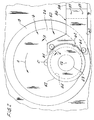
- the cross sectional profile of the polishing surface 26 of the polishing pad 16 is monitored to determine whether the profile of the polishing surface becomes more concave in shape than permitted by a process tolerance amount.
- the cross section profile of the pad when it has become concave is illustrated in Fig. 5A.
- TTV total thickness variation
- the rough polishing machine 10 is stopped with its polishing arm 20 in a position over the second wafer holding station 32, as is shown in Fig. 1.
- the arm 60 is bolted onto the bracket 58 mounted on the rough polishing machine 10 in a position for holding the pad shaping tool 52.
- the pad shaping tool is placed in the arcuate recess 62 of the arm 60 on top of the polishing pad 16 such that the pad shaping surface 54 extends across the entire radial width W of the polishing surface.
- the rotation of the polishing pad 16 is indicated by arrow A in Figs. 1 and 2.
- the direction of rotation drives the pad shaping tool 52 into the arcuate recess 62 and into engagement with the rollers 64.
- the tool 52 is constrained by the fixture 56 from rotating with the polishing pad 16 about its center of rotation C 1 .
- the center C 2 of the pad shaping tool 52 is held from substantial radial movement with respect to the center of rotation C 1 of the polishing pad 16.
- Contact of the tool 52 with the rotary pad 16 causes the tool to rotate about its center C 2 relative to the arm 60.
- the finish polishing machine 12 may continue operation while pad shaping on the rough polishing machine 10 begins. Once finish polishing of the wafer by the finish polishing machine is completed, the arm 40 of the finish polishing machine 12 places the wafer and polishing block on the exit station 46, and halts further operation.
- the shape of the pad shaping surface 54 of the pad shaping tool 52 is particularly suited for making the profile of the pad 16 more convex.
- the pad shaping tool 52 of the preferred embodiment abrades away more of the polishing pad 16 along the radially inner and outer margins, making the profile of the polishing surface 26 of the pad more nearly flat. It is envisioned that the abrasive pad shaping surface 54 on the tool 52 could be made in different configurations for reducing the convexity of the polishing surface 26.
- Pad shaping continues for a time determined by the operator based on the detected concavity of the pad shaping surface 26. A typical pad shaping time is about ten to thirty seconds, so that this shaping procedure does not seriously disrupt the polishing machine cycles.
- the flatter cross sectional profile of the polishing surface 26 after shaping is schematically illustrated in Fig. 5B.
- the polishing surface 26 may be given a slightly curvex profile (not shown) to permit greater intervals between pad shaping.
- the pad shaping tool 52 and fixture 56 are removed.
- a second plurality of wafers are then polished on the newly flattened polishing pad 16 in the same manner as the first plurality of wafers. The flatness of the second plurality of wafers is monitored until it is indicated that the pad 16 must be shaped again.
Landscapes
- Engineering & Computer Science (AREA)
- Mechanical Engineering (AREA)
- Finish Polishing, Edge Sharpening, And Grinding By Specific Grinding Devices (AREA)
- Mechanical Treatment Of Semiconductor (AREA)
- Polishing Bodies And Polishing Tools (AREA)
- Grinding And Polishing Of Tertiary Curved Surfaces And Surfaces With Complex Shapes (AREA)
- Grinding-Machine Dressing And Accessory Apparatuses (AREA)
Applications Claiming Priority (2)
| Application Number | Priority Date | Filing Date | Title |
|---|---|---|---|
| US639185 | 1996-04-26 | ||
| US08/639,185 US5840202A (en) | 1996-04-26 | 1996-04-26 | Apparatus and method for shaping polishing pads |
Publications (2)
| Publication Number | Publication Date |
|---|---|
| EP0803327A2 true EP0803327A2 (fr) | 1997-10-29 |
| EP0803327A3 EP0803327A3 (fr) | 1998-08-19 |
Family
ID=24563073
Family Applications (1)
| Application Number | Title | Priority Date | Filing Date |
|---|---|---|---|
| EP97302420A Withdrawn EP0803327A3 (fr) | 1996-04-26 | 1997-04-09 | Dispositif et procédé pour le profilage de patins de polissage |
Country Status (8)
| Country | Link |
|---|---|
| US (1) | US5840202A (fr) |
| EP (1) | EP0803327A3 (fr) |
| JP (1) | JPH1071558A (fr) |
| KR (1) | KR970072158A (fr) |
| CN (1) | CN1076249C (fr) |
| MY (1) | MY133665A (fr) |
| SG (1) | SG55295A1 (fr) |
| TW (1) | TW330881B (fr) |
Cited By (2)
| Publication number | Priority date | Publication date | Assignee | Title |
|---|---|---|---|---|
| US6120350A (en) * | 1999-03-31 | 2000-09-19 | Memc Electronic Materials, Inc. | Process for reconditioning polishing pads |
| WO2001032363A1 (fr) * | 1999-11-03 | 2001-05-10 | Memc Electronic Materials, Inc. | Procede permettant de determiner des caracteristiques de performance de tampons de polissage |
Families Citing this family (15)
| Publication number | Priority date | Publication date | Assignee | Title |
|---|---|---|---|---|
| JPH10235552A (ja) * | 1997-02-24 | 1998-09-08 | Ebara Corp | ポリッシング装置 |
| US6135863A (en) * | 1999-04-20 | 2000-10-24 | Memc Electronic Materials, Inc. | Method of conditioning wafer polishing pads |
| US6432823B1 (en) * | 1999-11-04 | 2002-08-13 | International Business Machines Corporation | Off-concentric polishing system design |
| KR100383324B1 (ko) * | 2000-11-24 | 2003-05-12 | 삼성전자주식회사 | 반도체 장치의 제조에서 연마 패드 검사 방법과 이를 수행하기 위한 검사 장치 및 이를 채용한 연마 장치. |
| JP4058904B2 (ja) * | 2000-12-19 | 2008-03-12 | 株式会社Sumco | 研磨布のドレッシング方法、半導体ウェーハの研磨方法及び研磨装置 |
| CN1792553B (zh) * | 2005-12-30 | 2010-05-12 | 广东工业大学 | 抛光垫修整装置及修整方法 |
| CN100441377C (zh) * | 2006-12-05 | 2008-12-10 | 中国科学院上海光学精密机械研究所 | 用于环行抛光机的校正板 |
| WO2015061006A1 (fr) * | 2013-10-23 | 2015-04-30 | Applied Materials, Inc. | Système de polissage à commande de vitesse de zone locale |
| US9751189B2 (en) | 2014-07-03 | 2017-09-05 | Applied Materials, Inc. | Compliant polishing pad and polishing module |
| WO2017165046A1 (fr) * | 2016-03-25 | 2017-09-28 | Applied Materials, Inc. | Système de polissage avec commande de débit par zone locale et mode d'oscillation |
| WO2017165068A1 (fr) * | 2016-03-25 | 2017-09-28 | Applied Materials, Inc. | Système de polissage de zone locale et ensembles tampon de polissage pour système de polissage |
| CN106078413B (zh) * | 2016-06-28 | 2018-12-25 | 东莞捷荣技术股份有限公司 | 一种平面打磨无动力辅助转动装置及打磨机 |
| US9802293B1 (en) * | 2016-09-29 | 2017-10-31 | Rohm And Haas Electronic Materials Cmp Holdings, Inc. | Method to shape the surface of chemical mechanical polishing pads |
| CN106392884B (zh) * | 2016-12-14 | 2019-10-18 | 北京中电科电子装备有限公司 | 一种砂轮的修整控制系统及方法 |
| JP6924710B2 (ja) * | 2018-01-09 | 2021-08-25 | 信越半導体株式会社 | 研磨装置および研磨方法 |
Family Cites Families (18)
| Publication number | Priority date | Publication date | Assignee | Title |
|---|---|---|---|---|
| CH640766A5 (en) * | 1981-07-16 | 1984-01-31 | Raymond Ansermoz | Lapping machine |
| JPS59129663A (ja) * | 1983-01-18 | 1984-07-26 | Toshiba Corp | ウエハラツピング装置 |
| JPS6190868A (ja) * | 1984-10-08 | 1986-05-09 | Toshiba Corp | 研磨装置 |
| US4720938A (en) * | 1986-07-31 | 1988-01-26 | General Signal Corp. | Dressing fixture |
| JPS63283859A (ja) * | 1987-05-13 | 1988-11-21 | Hitachi Ltd | ウェハ研磨用治具 |
| DE3926673A1 (de) * | 1989-08-11 | 1991-02-14 | Wacker Chemitronic | Verfahren und vorrichtung zur poliertuchaufbereitung beim chemomechanischen polieren, insbesondere von halbleiterscheiben |
| US5081051A (en) * | 1990-09-12 | 1992-01-14 | Intel Corporation | Method for conditioning the surface of a polishing pad |
| JP3173041B2 (ja) * | 1991-05-15 | 2001-06-04 | 不二越機械工業株式会社 | ドレッサー付きウェハー研磨装置及びその研磨布表面のドレッシング方法 |
| JPH05228829A (ja) * | 1992-02-19 | 1993-09-07 | Mitsubishi Materials Corp | ウェーハ研磨装置 |
| US5216843A (en) * | 1992-09-24 | 1993-06-08 | Intel Corporation | Polishing pad conditioning apparatus for wafer planarization process |
| US5384986A (en) * | 1992-09-24 | 1995-01-31 | Ebara Corporation | Polishing apparatus |
| JP2622069B2 (ja) * | 1993-06-30 | 1997-06-18 | 三菱マテリアル株式会社 | 研磨布のドレッシング装置 |
| US5456627A (en) * | 1993-12-20 | 1995-10-10 | Westech Systems, Inc. | Conditioner for a polishing pad and method therefor |
| US5486131A (en) * | 1994-01-04 | 1996-01-23 | Speedfam Corporation | Device for conditioning polishing pads |
| US5650039A (en) * | 1994-03-02 | 1997-07-22 | Applied Materials, Inc. | Chemical mechanical polishing apparatus with improved slurry distribution |
| JPH07299738A (ja) * | 1994-05-11 | 1995-11-14 | Mitsubishi Materials Corp | ウエハ研磨装置 |
| US5534106A (en) * | 1994-07-26 | 1996-07-09 | Kabushiki Kaisha Toshiba | Apparatus for processing semiconductor wafers |
| JP3637977B2 (ja) * | 1995-01-19 | 2005-04-13 | 株式会社荏原製作所 | ポリッシングの終点検知方法 |
-
1996
- 1996-04-26 US US08/639,185 patent/US5840202A/en not_active Expired - Lifetime
-
1997
- 1997-03-22 TW TW086103642A patent/TW330881B/zh active
- 1997-04-01 SG SG1997001022A patent/SG55295A1/en unknown
- 1997-04-09 MY MYPI97001528A patent/MY133665A/en unknown
- 1997-04-09 EP EP97302420A patent/EP0803327A3/fr not_active Withdrawn
- 1997-04-23 CN CN97110795A patent/CN1076249C/zh not_active Expired - Fee Related
- 1997-04-25 KR KR1019970015691A patent/KR970072158A/ko not_active Withdrawn
- 1997-04-25 JP JP10875797A patent/JPH1071558A/ja not_active Withdrawn
Cited By (4)
| Publication number | Priority date | Publication date | Assignee | Title |
|---|---|---|---|---|
| US6120350A (en) * | 1999-03-31 | 2000-09-19 | Memc Electronic Materials, Inc. | Process for reconditioning polishing pads |
| WO2000058053A1 (fr) * | 1999-03-31 | 2000-10-05 | Memc Electronic Materials, Inc. | Appareil et procede de remise en etat de tampons de polissage |
| WO2001032363A1 (fr) * | 1999-11-03 | 2001-05-10 | Memc Electronic Materials, Inc. | Procede permettant de determiner des caracteristiques de performance de tampons de polissage |
| US6293139B1 (en) | 1999-11-03 | 2001-09-25 | Memc Electronic Materials, Inc. | Method of determining performance characteristics of polishing pads |
Also Published As
| Publication number | Publication date |
|---|---|
| CN1167667A (zh) | 1997-12-17 |
| TW330881B (en) | 1998-05-01 |
| KR970072158A (ko) | 1997-11-07 |
| MY133665A (en) | 2007-11-30 |
| US5840202A (en) | 1998-11-24 |
| JPH1071558A (ja) | 1998-03-17 |
| CN1076249C (zh) | 2001-12-19 |
| SG55295A1 (en) | 1998-12-21 |
| EP0803327A3 (fr) | 1998-08-19 |
Similar Documents
| Publication | Publication Date | Title |
|---|---|---|
| US5840202A (en) | Apparatus and method for shaping polishing pads | |
| US6120350A (en) | Process for reconditioning polishing pads | |
| US6517414B1 (en) | Method and apparatus for controlling a pad conditioning process of a chemical-mechanical polishing apparatus | |
| EP1063056A2 (fr) | Procédé et dispositif pour mesurer le profil d'un tampon de polissage et commande en boucle fermée du processus de dressage d'un tampon | |
| US6102777A (en) | Lapping apparatus and method for high speed lapping with a rotatable abrasive platen | |
| EP0816017B1 (fr) | Procédé et dispositif de dressage d'une toile de polissage | |
| KR100449630B1 (ko) | 화학기계적 연마장치의 연마패드 컨디셔닝 장치 | |
| EP1270148A1 (fr) | Procédé et appareil de conditionnement d'un tampon a polir | |
| US6733370B2 (en) | In-situ pad conditioning apparatus for CMP polisher | |
| US6394886B1 (en) | Conformal disk holder for CMP pad conditioner | |
| WO2001027350A1 (fr) | Decalage, dimensions et forme optimales d'un tampon destine au polissage et a l'aplanissement chimico-mecanique | |
| EP1171264A1 (fr) | Procede de traitement de tampons de polissage de tranches | |
| JP3640504B2 (ja) | ドレッシング方法及び装置 | |
| KR20010107761A (ko) | 폴리싱방법 및 폴리싱장치 | |
| WO2001058644A1 (fr) | Procede et appareil de commande d'un procede de conditionnement de tampons d'un appareil de polissage chimique et mecanique | |
| US6857942B1 (en) | Apparatus and method for pre-conditioning a conditioning disc | |
| US6300248B1 (en) | On-chip pad conditioning for chemical mechanical polishing | |
| EP0769350A1 (fr) | Procédé et dispositif pour dresser un tissu de polissage | |
| US20040224617A1 (en) | Static pad conditioner | |
| JPH1110521A (ja) | ウェーハ研磨装置 | |
| KR100481553B1 (ko) | 평탄화 장치 | |
| JPH10128653A (ja) | ウエハ研磨装置及びウエハ研磨方法 | |
| JPH10118913A (ja) | 平面研磨方法及び平面研磨装置 | |
| JPH07299731A (ja) | ウエハ研磨装置および研磨面のドレッシング方法 |
Legal Events
| Date | Code | Title | Description |
|---|---|---|---|
| PUAI | Public reference made under article 153(3) epc to a published international application that has entered the european phase |
Free format text: ORIGINAL CODE: 0009012 |
|
| AK | Designated contracting states |
Kind code of ref document: A2 Designated state(s): DE FR GB IT |
|
| PUAL | Search report despatched |
Free format text: ORIGINAL CODE: 0009013 |
|
| AK | Designated contracting states |
Kind code of ref document: A3 Designated state(s): DE FR GB IT |
|
| 17P | Request for examination filed |
Effective date: 19981207 |
|
| 17Q | First examination report despatched |
Effective date: 20001009 |
|
| STAA | Information on the status of an ep patent application or granted ep patent |
Free format text: STATUS: THE APPLICATION IS DEEMED TO BE WITHDRAWN |
|
| 18D | Application deemed to be withdrawn |
Effective date: 20010220 |