EP0802566A2 - Halbleiterbauteil, Verbindungsmethode und Halbleiterbauteil-Verbinder - Google Patents
Halbleiterbauteil, Verbindungsmethode und Halbleiterbauteil-Verbinder Download PDFInfo
- Publication number
- EP0802566A2 EP0802566A2 EP96110808A EP96110808A EP0802566A2 EP 0802566 A2 EP0802566 A2 EP 0802566A2 EP 96110808 A EP96110808 A EP 96110808A EP 96110808 A EP96110808 A EP 96110808A EP 0802566 A2 EP0802566 A2 EP 0802566A2
- Authority
- EP
- European Patent Office
- Prior art keywords
- package
- semiconductor devices
- exposed terminals
- terminals
- semiconductor
- Prior art date
- Legal status (The legal status is an assumption and is not a legal conclusion. Google has not performed a legal analysis and makes no representation as to the accuracy of the status listed.)
- Granted
Links
Images


Classifications
-
- H—ELECTRICITY
- H05—ELECTRIC TECHNIQUES NOT OTHERWISE PROVIDED FOR
- H05K—PRINTED CIRCUITS; CASINGS OR CONSTRUCTIONAL DETAILS OF ELECTRIC APPARATUS; MANUFACTURE OF ASSEMBLAGES OF ELECTRICAL COMPONENTS
- H05K7/00—Constructional details common to different types of electric apparatus
- H05K7/02—Arrangements of circuit components or wiring on supporting structure
- H05K7/023—Stackable modules
-
- H—ELECTRICITY
- H10—SEMICONDUCTOR DEVICES; ELECTRIC SOLID-STATE DEVICES NOT OTHERWISE PROVIDED FOR
- H10W—GENERIC PACKAGES, INTERCONNECTIONS, CONNECTORS OR OTHER CONSTRUCTIONAL DETAILS OF DEVICES COVERED BY CLASS H10
- H10W78/00—Detachable holders for supporting packaged chips in operation
-
- H—ELECTRICITY
- H10—SEMICONDUCTOR DEVICES; ELECTRIC SOLID-STATE DEVICES NOT OTHERWISE PROVIDED FOR
- H10W—GENERIC PACKAGES, INTERCONNECTIONS, CONNECTORS OR OTHER CONSTRUCTIONAL DETAILS OF DEVICES COVERED BY CLASS H10
- H10W90/00—Package configurations
-
- H—ELECTRICITY
- H01—ELECTRIC ELEMENTS
- H01R—ELECTRICALLY-CONDUCTIVE CONNECTIONS; STRUCTURAL ASSOCIATIONS OF A PLURALITY OF MUTUALLY-INSULATED ELECTRICAL CONNECTING ELEMENTS; COUPLING DEVICES; CURRENT COLLECTORS
- H01R12/00—Structural associations of a plurality of mutually-insulated electrical connecting elements, specially adapted for printed circuits, e.g. printed circuit boards [PCB], flat or ribbon cables, or like generally planar structures, e.g. terminal strips, terminal blocks; Coupling devices specially adapted for printed circuits, flat or ribbon cables, or like generally planar structures; Terminals specially adapted for contact with, or insertion into, printed circuits, flat or ribbon cables, or like generally planar structures
- H01R12/50—Fixed connections
- H01R12/51—Fixed connections for rigid printed circuits or like structures
- H01R12/52—Fixed connections for rigid printed circuits or like structures connecting to other rigid printed circuits or like structures
-
- H—ELECTRICITY
- H01—ELECTRIC ELEMENTS
- H01R—ELECTRICALLY-CONDUCTIVE CONNECTIONS; STRUCTURAL ASSOCIATIONS OF A PLURALITY OF MUTUALLY-INSULATED ELECTRICAL CONNECTING ELEMENTS; COUPLING DEVICES; CURRENT COLLECTORS
- H01R12/00—Structural associations of a plurality of mutually-insulated electrical connecting elements, specially adapted for printed circuits, e.g. printed circuit boards [PCB], flat or ribbon cables, or like generally planar structures, e.g. terminal strips, terminal blocks; Coupling devices specially adapted for printed circuits, flat or ribbon cables, or like generally planar structures; Terminals specially adapted for contact with, or insertion into, printed circuits, flat or ribbon cables, or like generally planar structures
- H01R12/70—Coupling devices
- H01R12/71—Coupling devices for rigid printing circuits or like structures
- H01R12/712—Coupling devices for rigid printing circuits or like structures co-operating with the surface of the printed circuit or with a coupling device exclusively provided on the surface of the printed circuit
- H01R12/714—Coupling devices for rigid printing circuits or like structures co-operating with the surface of the printed circuit or with a coupling device exclusively provided on the surface of the printed circuit with contacts abutting directly the printed circuit; Button contacts therefore provided on the printed circuit
-
- H—ELECTRICITY
- H01—ELECTRIC ELEMENTS
- H01R—ELECTRICALLY-CONDUCTIVE CONNECTIONS; STRUCTURAL ASSOCIATIONS OF A PLURALITY OF MUTUALLY-INSULATED ELECTRICAL CONNECTING ELEMENTS; COUPLING DEVICES; CURRENT COLLECTORS
- H01R13/00—Details of coupling devices of the kinds covered by groups H01R12/70 or H01R24/00 - H01R33/00
- H01R13/02—Contact members
- H01R13/22—Contacts for co-operating by abutting
- H01R13/24—Contacts for co-operating by abutting resilient; resiliently-mounted
- H01R13/2407—Contacts for co-operating by abutting resilient; resiliently-mounted characterized by the resilient means
- H01R13/2421—Contacts for co-operating by abutting resilient; resiliently-mounted characterized by the resilient means using coil springs
-
- H—ELECTRICITY
- H05—ELECTRIC TECHNIQUES NOT OTHERWISE PROVIDED FOR
- H05K—PRINTED CIRCUITS; CASINGS OR CONSTRUCTIONAL DETAILS OF ELECTRIC APPARATUS; MANUFACTURE OF ASSEMBLAGES OF ELECTRICAL COMPONENTS
- H05K1/00—Printed circuits
- H05K1/02—Details
- H05K1/14—Structural association of two or more printed circuits
- H05K1/148—Arrangements of two or more hingeably connected rigid printed circuit boards, i.e. connected by flexible means
-
- H—ELECTRICITY
- H05—ELECTRIC TECHNIQUES NOT OTHERWISE PROVIDED FOR
- H05K—PRINTED CIRCUITS; CASINGS OR CONSTRUCTIONAL DETAILS OF ELECTRIC APPARATUS; MANUFACTURE OF ASSEMBLAGES OF ELECTRICAL COMPONENTS
- H05K1/00—Printed circuits
- H05K1/18—Printed circuits structurally associated with non-printed electric components
- H05K1/182—Printed circuits structurally associated with non-printed electric components associated with components mounted in printed circuit boards [PCB], e.g. insert-mounted components [IMC]
- H05K1/185—Printed circuits structurally associated with non-printed electric components associated with components mounted in printed circuit boards [PCB], e.g. insert-mounted components [IMC] associated with components encapsulated in the insulating substrate of the PCBs; associated with components incorporated in internal layers of multilayer circuit boards
-
- H—ELECTRICITY
- H05—ELECTRIC TECHNIQUES NOT OTHERWISE PROVIDED FOR
- H05K—PRINTED CIRCUITS; CASINGS OR CONSTRUCTIONAL DETAILS OF ELECTRIC APPARATUS; MANUFACTURE OF ASSEMBLAGES OF ELECTRICAL COMPONENTS
- H05K3/00—Apparatus or processes for manufacturing printed circuits
- H05K3/22—Secondary treatment of printed circuits
- H05K3/28—Applying non-metallic protective coatings
- H05K3/284—Applying non-metallic protective coatings for encapsulating mounted components
-
- H—ELECTRICITY
- H10—SEMICONDUCTOR DEVICES; ELECTRIC SOLID-STATE DEVICES NOT OTHERWISE PROVIDED FOR
- H10W—GENERIC PACKAGES, INTERCONNECTIONS, CONNECTORS OR OTHER CONSTRUCTIONAL DETAILS OF DEVICES COVERED BY CLASS H10
- H10W46/00—Marks applied to devices, e.g. for alignment or identification
-
- H—ELECTRICITY
- H10—SEMICONDUCTOR DEVICES; ELECTRIC SOLID-STATE DEVICES NOT OTHERWISE PROVIDED FOR
- H10W—GENERIC PACKAGES, INTERCONNECTIONS, CONNECTORS OR OTHER CONSTRUCTIONAL DETAILS OF DEVICES COVERED BY CLASS H10
- H10W70/00—Package substrates; Interposers; Redistribution layers [RDL]
- H10W70/60—Insulating or insulated package substrates; Interposers; Redistribution layers
-
- H—ELECTRICITY
- H10—SEMICONDUCTOR DEVICES; ELECTRIC SOLID-STATE DEVICES NOT OTHERWISE PROVIDED FOR
- H10W—GENERIC PACKAGES, INTERCONNECTIONS, CONNECTORS OR OTHER CONSTRUCTIONAL DETAILS OF DEVICES COVERED BY CLASS H10
- H10W72/00—Interconnections or connectors in packages
- H10W72/01—Manufacture or treatment
-
- H—ELECTRICITY
- H10—SEMICONDUCTOR DEVICES; ELECTRIC SOLID-STATE DEVICES NOT OTHERWISE PROVIDED FOR
- H10W—GENERIC PACKAGES, INTERCONNECTIONS, CONNECTORS OR OTHER CONSTRUCTIONAL DETAILS OF DEVICES COVERED BY CLASS H10
- H10W72/00—Interconnections or connectors in packages
- H10W72/60—Strap connectors, e.g. thick copper clips for grounding of power devices
-
- H—ELECTRICITY
- H10—SEMICONDUCTOR DEVICES; ELECTRIC SOLID-STATE DEVICES NOT OTHERWISE PROVIDED FOR
- H10W—GENERIC PACKAGES, INTERCONNECTIONS, CONNECTORS OR OTHER CONSTRUCTIONAL DETAILS OF DEVICES COVERED BY CLASS H10
- H10W74/00—Encapsulations, e.g. protective coatings
-
- H—ELECTRICITY
- H10—SEMICONDUCTOR DEVICES; ELECTRIC SOLID-STATE DEVICES NOT OTHERWISE PROVIDED FOR
- H10W—GENERIC PACKAGES, INTERCONNECTIONS, CONNECTORS OR OTHER CONSTRUCTIONAL DETAILS OF DEVICES COVERED BY CLASS H10
- H10W90/00—Package configurations
- H10W90/20—Configurations of stacked chips
-
- H—ELECTRICITY
- H10—SEMICONDUCTOR DEVICES; ELECTRIC SOLID-STATE DEVICES NOT OTHERWISE PROVIDED FOR
- H10W—GENERIC PACKAGES, INTERCONNECTIONS, CONNECTORS OR OTHER CONSTRUCTIONAL DETAILS OF DEVICES COVERED BY CLASS H10
- H10W90/00—Package configurations
- H10W90/20—Configurations of stacked chips
- H10W90/22—Configurations of stacked chips the stacked chips being on both top and bottom sides of a package substrate, interposer or RDL
-
- H—ELECTRICITY
- H10—SEMICONDUCTOR DEVICES; ELECTRIC SOLID-STATE DEVICES NOT OTHERWISE PROVIDED FOR
- H10W—GENERIC PACKAGES, INTERCONNECTIONS, CONNECTORS OR OTHER CONSTRUCTIONAL DETAILS OF DEVICES COVERED BY CLASS H10
- H10W90/00—Package configurations
- H10W90/20—Configurations of stacked chips
- H10W90/231—Configurations of stacked chips the stacked chips being on both top and bottom sides of an auxiliary carrier having no electrical connection structure
-
- H—ELECTRICITY
- H10—SEMICONDUCTOR DEVICES; ELECTRIC SOLID-STATE DEVICES NOT OTHERWISE PROVIDED FOR
- H10W—GENERIC PACKAGES, INTERCONNECTIONS, CONNECTORS OR OTHER CONSTRUCTIONAL DETAILS OF DEVICES COVERED BY CLASS H10
- H10W90/00—Package configurations
- H10W90/20—Configurations of stacked chips
- H10W90/291—Configurations of stacked chips characterised by containers, encapsulations, or other housings for the stacked chips
-
- H—ELECTRICITY
- H10—SEMICONDUCTOR DEVICES; ELECTRIC SOLID-STATE DEVICES NOT OTHERWISE PROVIDED FOR
- H10W—GENERIC PACKAGES, INTERCONNECTIONS, CONNECTORS OR OTHER CONSTRUCTIONAL DETAILS OF DEVICES COVERED BY CLASS H10
- H10W90/00—Package configurations
- H10W90/20—Configurations of stacked chips
- H10W90/297—Configurations of stacked chips characterised by the through-semiconductor vias [TSVs] in the stacked chips
-
- H—ELECTRICITY
- H10—SEMICONDUCTOR DEVICES; ELECTRIC SOLID-STATE DEVICES NOT OTHERWISE PROVIDED FOR
- H10W—GENERIC PACKAGES, INTERCONNECTIONS, CONNECTORS OR OTHER CONSTRUCTIONAL DETAILS OF DEVICES COVERED BY CLASS H10
- H10W90/00—Package configurations
- H10W90/701—Package configurations characterised by the relative positions of pads or connectors relative to package parts
- H10W90/721—Package configurations characterised by the relative positions of pads or connectors relative to package parts of bump connectors
-
- H—ELECTRICITY
- H10—SEMICONDUCTOR DEVICES; ELECTRIC SOLID-STATE DEVICES NOT OTHERWISE PROVIDED FOR
- H10W—GENERIC PACKAGES, INTERCONNECTIONS, CONNECTORS OR OTHER CONSTRUCTIONAL DETAILS OF DEVICES COVERED BY CLASS H10
- H10W90/00—Package configurations
- H10W90/701—Package configurations characterised by the relative positions of pads or connectors relative to package parts
- H10W90/751—Package configurations characterised by the relative positions of pads or connectors relative to package parts of bond wires
- H10W90/754—Package configurations characterised by the relative positions of pads or connectors relative to package parts of bond wires between a chip and a stacked insulating package substrate, interposer or RDL
Definitions
- This invention relates to semiconductor devices with semiconductor elements enclosed in packages, methods of electrically connecting such semiconductor devices, and semiconductor device connectors.
- the invention relates to a technique of packaging semiconductor devices in high density.
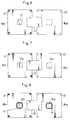
- a package 201 has a semiconductor element 202 enclosed therein, and numerous lead terminals 203 extending from all sides of the package 201 for connection to an external.
- the QFP is mounted on a carrier board 204 with the lead terminals 203 soldered to wiring patterns 205.
- a package 211 has a semiconductor element 212 enclosed therein, and numerous solder balls 213 arranged two-dimensionally on a back side surface of the package 211 for connection to an external.
- the BGA is mounted on a carrier board 214 with the solder balls 213 reflow-soldered to wiring patterns 215.
- This invention has been made having regard to the state of the art noted above, and has for a primary object to provide semiconductor devices suited for high-density packaging and for shortening wiring between the semiconductor devices.
- Another object of this invention is to provide a method of connecting such semiconductor devices.
- a further object of this invention is to provide connectors for connecting such semiconductor devices.
- a semiconductor device comprising:
- Semiconductor devices according to this invention are assembled three-dimensionally by arranging the devices such that front side surfaces or rear side surfaces of the packages defining the exposed terminals for external connection are in an opposed relationship.
- the exposed terminals in the opposed relationship of adjacent semiconductor devices are connected to each other.
- An area of the board occupied by these semiconductor devices corresponds to an installation area where the semiconductor devices assembled three-dimensionally contact the carrier board.
- This area occupied by the semiconductor devices is far smaller than an area occupied by conventional QFP or BGA devices mounted in horizontal posture on a carrier board.
- only short wirings are required to interconnect the exposed terminals. This provides the advantage of diminishing stray capacitance and parasitic inductance of wirings which hamper high-speed processing.
- the package includes package bases defining the opposite surfaces thereof, respectively, the exposed terminals for external connection being formed on outer surfaces of the package bases, the semiconductor element being die-bonded to an inner surface of at least one of the package bases.
- This construction facilitates fabrication of the semiconductor devices each having exposed terminals arranged on the opposite surfaces of the package.
- a sealing synthetic resin may be filled into a space between the package bases to secure reliability of the semiconductor device.
- the package bases are electrically interconnected through a flexible printed circuit board defining a plurality of wiring patterns, the wiring patterns being connected at first ends thereof to internal terminals formed on an inner surface of one of the package bases, and at second ends thereof to internal terminals formed on an inner surface of the other of the package bases.
- This construction facilitates electrical connection between the two package bases.
- This invention also provides a method of electrically connecting a plurality of semiconductor devices each having at least one semiconductor element enclosed in a package, a plurality of exposed terminals for external connection arranged two-dimensionally on each of opposite surfaces of the package, and internal wiring for interconnecting the semiconductor element and the exposed terminals for external connection on the opposite surfaces of the package, the method comprising:
- the semiconductor devices are arranged in an opposed relationship and at fixed intervals, with the conductive connecting elements interposed between an adjacent pair of the semiconductor devices to interconnect the exposed terminals of one semiconductor device and the exposed terminals of another semiconductor device.
- the semiconductor devices assembled in this way occupy only a very small area of a carrier board.
- the conductive connecting elements may have a minimal length for interconnecting the exposed terminals of the two semiconductor devices.
- the conductive connecting elements may, for example, be connecting pins having opposite ends thereof elastically contacting the exposed terminals opposed to each other.
- the conductive connecting elements may be connecting pins having opposite ends thereof joined by a joining material to the exposed terminals opposed to each other.
- a connector assembly for electrically connecting a plurality of semiconductor devices each having at least one semiconductor element enclosed in a package, a plurality of exposed terminals for external connection arranged two-dimensionally on each of opposite surfaces of the package, and internal wiring for interconnecting the semiconductor element and the exposed terminals for external connection on the opposite surfaces of the package.
- the connector assembly comprises a plurality of connectors each including:
- each connector is interposed between an adjacent pair of semiconductor devices.
- the base plate has conductive connecting elements in the same arrangement as the exposed terminals of the semiconductor devices.
- the conductive connecting elements extend through the base plate to project from the opposite surfaces thereof.
- the exposed terminals of an adjacent pair of semiconductor devices are electrically interconnected through the conductive connecting elements of the connector.
- the semiconductor devices may be assembled in high density by interposing therebetween the connector according to this invention.
- the conductive connecting elements for electrically interconnecting the exposed terminals of adjacent semiconductor devices may have a minimal length to minimize the influences of stray capacitance and parasitic inductance of wirings (connecting elements) which hamper high-speed processing of the semiconductor devices.
- the base plate includes a positioning structure for positioning the semiconductor devices such that the exposed terminals register with the conductive connecting elements.
- This construction facilitates a positional adjustment between the exposed terminals of the semiconductor devices and the conductive connecting elements of the connector.
- the base plate includes external connection terminals arranged on at least one side surface thereof.
- the external connection terminals may be used to facilitate connection to the wiring patterns on the carrier board.
- the conductive connecting elements may, for example, be axially elastic connecting pins having opposite ends thereof elastically contacting the exposed terminals of the semiconductor devices opposed to each other. According to this construction, the connectors and semiconductor devices are only in elastic contact with each other. Any semiconductor device failing to function properly after mounting on a carrier board may be replaced with ease.
- the connector assembly further comprises a coupling structure for rigidly coupling the base plates arranged in a direction of thickness thereof, with the semiconductor devices interposed therebetween.
- This coupling structure assures the elastic contact between the elastic connecting pins and the exposed terminals of the semiconductor devices. Any semiconductor device may be replaced with ease by undoing the coupling structure.
- each of the elastic connecting pins includes a conductive tube opening at opposite ends thereof, a pair of conductive contacts disposed in opposite end regions of the tube to be movable longitudinally thereof, the contacts being retained in the tube with only tip ends of the contacts projectable from the opposite ends, respectively, and a biasing element mounted in the tube for biasing the contacts in directions to project the tip ends from the opposite ends.
- the conductive connecting elements may be connecting pins in form of metal rods having opposite ends thereof joined through a joining material to the exposed terminals of the semiconductor devices opposed to each other.
- Such a connector has a simplified construction, and yet assures the electrical connection between semiconductor device and connector.
- the connecting pins in form of metal rods have solder balls formed at opposite ends thereof.
- solder balls may be formed easily by electroplating. This involves a less chance of adversely affecting the semiconductor devices than where solder balls are formed by electroplating on the exposed terminals of the semiconductor devices.
- the conductive connecting elements may be through hole platings formed by plating a metal in bores of the base plate.
- the through hole platings have opposite ends thereof joined through a joining material to the exposed terminals of the semiconductor devices opposed to each other.
- a semiconductor device according to this invention will be described first.
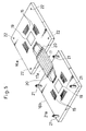
- Fig. 3 is a perspective view showing an outward appearance of a semiconductor device embodying this invention.
- Fig. 4 is a sectional view of the semiconductor device shown in Fig. 3.
- a semiconductor device 10 has a rectangular package 11.
- the package 11 is about 10 to 50mm long in one side, and about 2 to 8mm thick.
- the package 11 is not limited to the rectangular shape but may be disk-shaped, for example.
- the package 11 encloses at least one semiconductor element. In this embodiment, two semiconductor elements 12a and 12b are enclosed therein.
- the package 11 includes a plurality of exposed terminals 13 for connection to an external, arranged two-dimensionally on a front side surface 11a and a back side surface 11b thereof.
- the exposed terminals 13 are about 0.3 to 1.2mm in diameter, and are arranged at intervals of about 0.5 to 1.5mm.
- the semiconductor elements 12a and 12b and the exposed terminals 13 on opposite surfaces 11a and 11b of package 11 are interconnected through internal wiring such as fine metal lines 14 and multi-layer wiring patterns 15.
- the semiconductor device 10 in this embodiment includes package bases 16a and 16b defining the opposite surfaces 11a and 11b of package 11.
- the package bases 16a and 16b are formed of ceramic, an epoxy resin or the like.
- the exposed terminals 13 are formed on outer surfaces of the package bases 16a and 16b (i.e. the opposite surfaces 11a and 11b of package 11).
- the semiconductor elements 12a and 12b are die-bonded by a conductive epoxy resin or the like to inner surfaces of the package bases 16a and 16b, respectively.
- the package bases 16a and 16b are interconnected inside the package 11 through a flexible printed circuit board 17. A space between the package bases 16a and 16b is filled with an insulating epoxy resin 18, for example.
- package bases 16a and 16b defining through holes and multi-layer wiring are prepared.
- the exposed terminals 13 are already formed on the outer surfaces (back side surfaces in Fig. 5) of the package bases 16a and 16b.
- the package bases 16a and 16b define die pads 19 centrally of the inner surfaces thereof, respectively, for die-bonding the semiconductor elements 12a and 12b.
- Ends of a plurality of wiring patterns 15 are arranged around each die pad 19.
- the other ends of wiring patterns 15 are connected to the exposed terminals 13 through the multi-layer wiring and through holes formed in the package bases 16a and 16b. Part of the other ends are connected to internal connection terminals 20 formed on the inner surface adjacent one side of each package base 16a or 16b.
- the flexible printed circuit board 17 defining wiring patterns 17a extends between the internal connection terminals 20 of the two package bases 16a and 16b.
- the package base 16b includes pins 21 erected at the four corners of the inner surface thereof.
- Each pin 21 has a projection 21a formed at a free end thereof.
- the package base 16a defines holes 22 at the four corners of the inner surface thereof for fitting tight with the projections 21a.
- the semiconductor element 12b is die-bonded with a conductive epoxy resin on the die pad 19 of the package base 16b. Further, as shown in Fig. 7, the semiconductor element 12a is likewise die-bonded on the die pad 19 of the package base 16a.
- fine metal lines 14 are formed for wire-bonding between the ends of wiring patterns 15 and bonding pads of the semiconductor element 12b on the package base 16b.
- the semiconductor element 12a on the package base 16a is wire-bonded similarly.
- protective films 23 are formed by potting an insulating epoxy resin or the like over the semiconductor elements 12a and 12b and fine metal lines 14.
- the two package bases 16a and 16b are assembled to extend parallel to each other as vertically spaced by the pins 21, with the holes 22 at the four corners of the package base 16b fitted on the projections 21a of the pins 21 on the package base 16b.
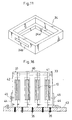
- the assembly is placed in a square frame 24 for use in resin injection.
- the frame 24 is vertically open, and has a supporting shoulder 24a formed around a lower inner surface thereof.
- One side of the frame 24 is perforated to define a resin inlet 24b.
- the two package bases 16a and 16b are placed in the frame 24, with the package base 16b supported at peripheries thereof by the supporting shoulder 24a.
- the space between the package bases 16a and 16b is filled with the insulating epoxy resin 18 introduced through the resin inlet 24b.
- the package 11 is removed from the frame 24 to obtain the semiconductor device 10 shown in Fig. 3.
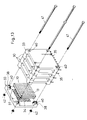
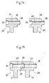
- Fig. 12 is a perspective view of the connectors embodying this invention.
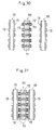
- Fig. 13 is an exploded perspective view showing use of the connectors.
- Figs. 14 and 15 are fragmentary sectional views showing a connector coupling structure.
- Fig. 16 is a front view, partly in section, of the semiconductor devices mounted on a carrier board.
- each connector 30 includes a rectangular base plate 31, and a plurality of connecting pins 32 extending through the base plate 31 to project from opposite surfaces thereof.
- the base plate 31 is formed of an insulating synthetic resin. From the viewpoint of enhanced heat radiation of the connector 30, the base plate 31 may be formed of aluminum and covered with an insulating film.
- the connecting pins 32 are elastic axially thereof. Details of the connecting pins 32 will be described later.
- the connecting pins 32 are arranged two-dimensionally at the intervals corresponding to those of the exposed terminals 13 of the semiconductor device 10. When the semiconductor device 10 is sandwiched between two connectors 30, the connecting pins 32 of the respective connectors 30 press on the exposed terminals 13 on the opposite surfaces of the semiconductor device 10.
- These connecting pins 32 correspond to the conductive connecting elements of this invention.
- such connectors 30 may be interposed between a plurality of semiconductor devices 10 to realize a high-density package of semiconductor devices 10 (four devices in Fig. 13).
- the connecting pins 32 project from the opposite surfaces of each of the three intermediate connectors 30 shown in Fig. 13, since each is flanked by semiconductor devices 10.
- Each end connector 33 has connecting pins 34 projecting from only an inward surface thereof since only the inward surface is opposed to one of the semiconductor devices 10.
- the connectors 30 having the connecting pins 32 projecting from the opposite surfaces thereof may be used at the ends.
- a plurality of terminals 35 for external connection extend from a lower surface of the base plate 31 of each connector 30 or 33. These terminals 35 are electrically connected to wiring patterns formed on a carrier board when a plurality of semiconductor devices 10 are mounted on the carrier board by means of the connectors 30 and 33. The terminals 35 are electrically connected to appropriate connecting pins 32. A specific construction of terminals 35 will be described later.
- the base plate 31 of each connector 30 has a positioning structure for positioning the semiconductor devices 10 such that the exposed terminals 13 of the semiconductor devices 10 register with the connecting pins 32 of the connector 30.
- the positioning structure is in the form of square blocks 36 formed at the four corners of the base plate 31, with a stepped cutout 37 formed in an inward corner of each block 36. The corners of each semiconductor device 10 are fitted into the cutouts 37 to place the exposed terminals 13 in register with the connecting pins 32. Similar cutouts 37 are formed in each end connector 33 also.
- each connector 30 has a coupling structure for rigidly coupling a plurality of connectors 30 in the direction of their thickness, with semiconductor devices 10 sandwiched therebetween.
- each of the four square blocks 36 has a projection 38 formed on one surface thereof, and a recess 39 formed on the opposite surface for receiving the projection 38 of an adjacent connector 30.
- the projection 38 and recess 39 are penetrated by a bore 40.
- Similar projections 38, recesses 39 and bores 40 are formed on each end connector 33 also.
- a plurality of connectors 30 and 33 are coupled with the semiconductor devices 10 sandwiched therebetween, by fitting the projections 38 of one connector 30 into the recesses 39 of an opposed one of the connectors 30.
- bolts 41 are passed through the four bores 40 of each connector 30 or 33, and nuts 42 are screwed thereon to tighten the connectors 30 and 33 together.
- four semiconductor devices 10 are connected. The number of semiconductor devices 10 may of course be varied.
- the connectors 30 and 33 assembled to form a three-dimensional unit with a plurality of semiconductor devices 10 sandwiched therebetween are mounted on a carrier board 43 as shown in Fig. 16.
- the connectors 30 and 33 integrated are fixed to the carrier board 43 by means of L-shaped metal fittings 44 and screws 45, with the external connection terminals 35 soldered to wiring patterns on the carrier board 43.
- this mode of mounting to the carrier board 43 is not limitative.
- the connectors 30 and 33 integrated may be stacked one over the other on the carrier board 43.
- each connecting pin 32 has a conductive tube 46 opening at opposite ends thereof, and conductive contacts 47 mounted in the tube 46 to be movable longitudinally thereof.
- the tube 46 contains a coil spring 48 for outwardly biasing the contacts 47. Under the biasing force of the spring 48, distal ends of the respective contacts 47 project from the end openings of the tube 46.
- the contacts 47 have large diameter proximal ends to prevent the contacts 47 from falling off the tube 46.
- each connecting pin 32 is about 3 to 5mm long, and about 0.6 to 0.7mm in outside diameter.
- Each contact 47 is about 0.2 to 0.3mm in diameter.
- the length of the distal end of each contact 47 projecting from the opening of the tube 46, i.e. a range of movement (or stroke) of each contact 47, is about 0.6 to 0.8mm. With this relatively large range of movement, the contacts 47 may reliably be pressed into contact with the exposed terminals 13 formed on the semiconductor devices 10 even if variations should occur in the height of exposed terminals 13.
- each contact 47 defines a centrally recessed end surface 47a. This shape is selected in order to increase a pressure of elastic contact between the end surface 47a of the contact 47 and one of the exposed terminals 13 formed on semiconductor device 10, to assure an electrical connection therebetween.
- Other desirable shapes of the end surface 47a of each contact 47 are spherical as shown in Fig. 20B, and jagged as shown in Fig. 20C.
- Fig. 19 shows a structure for mounting each connecting pin 32 in the base plate 31 of the connector 30.
- the base plate 31 is formed of two plate members 31a and 31b joined together. Before joining the plate members 31a and 31b, bores are formed therein for receiving the connecting pins 32. The bores are slightly enlarged at openings thereof in opposed mating surfaces of the two plate members 31a and 31b to define stepped structures for fitting with a flange 46a formed on the tube 46 of each connecting pin 32. One end of each connecting pin 32 is inserted into one of the bores of one plate member 31a, and then the other plate member 31b is placed thereon with the other end of the connecting pin 32 extending into one of the bores thereof. An appropriate adhesive is applied to the mating surfaces of the plate members 31a and 31b, to obtain the integrated base plate 31 with the connecting pins 32 fixed in place by the plate members 31a and 31b.
- Fig. 21 shows a connecting pin 34 of each end connector 33.
- each connecting pin 34 has a bottomed tube 49 opening only at one end thereof, and one contact 50 axially movably mounted therein.
- the tube 49 contains a coil spring 51 for biasing the contact 50, so that a distal end of the contact 50 projects from the opening of the tube 49.
- the connecting pin 32 shown in Fig. 19 the connecting pin 34 also is secured to the base plate 31 formed of two plate members joined together. However, in the case of each end connector 33, bores are formed only in the inner plate member for receiving the connecting pins 34.
- the terminals 35 for external connection are connected, such as by welding, to the tubes 46 of the connecting pins 32 beforehand, which are to form a lowermost array in the base plate 31.
- Such integrated connecting pins 32 and terminals 35 are assembled to the base plate 31.
- the terminals 35 for external connection are connected to the tubes 49 of the connecting pins 34 beforehand, which are to form a lowermost array in the base plate 31.
- Such integrated connecting pins 34 and terminals 35 are assembled to the base plate 31.
- connection structures between the terminals 35 for external connection and connecting pins 32 and 34 are not limited to the above example.
- through hole plating is applied to the bore of at least one of the plate members 31a and 31b constituting the base plate 31 as described with reference to Fig. 19.
- Printed circuit patterns are formed on the mating surface of plate member 31a or 31b. One end of each printed circuit pattern is connected to the through hole plating, with the other end of the circuit pattern extending toward the terminal 35. The other end is connected, such as by soldering, to one of the terminals 35.
- the connecting pins 32 and 34 regardless of their positions in the two-dimensional arrangement may be electrically connected to the terminals 35 for external connection.
- the exposed terminals 13 of an adjacent pair of semiconductor devices 10 are interconnected through the connecting pins 32 or 34.
- These connecting pins 32 and 34 are extremely short (about 4 to 6mm) to minimize stray capacitance and parasitic inductance.
- a plurality of semiconductor devices 10 arranged in an opposed relationship readily realize a high-density packaging.
- the connectors 30 and 33 are disconnectable simply by removing the coupling bolts 41 shown in Figs. 13 and 16. Thus, when one of the semiconductor devices 10 should fail, the defective device 10 may be replaced and repackaged with ease.
Landscapes
- Engineering & Computer Science (AREA)
- Microelectronics & Electronic Packaging (AREA)
- Coupling Device And Connection With Printed Circuit (AREA)
- Connecting Device With Holders (AREA)
- Wire Bonding (AREA)
Applications Claiming Priority (3)
| Application Number | Priority Date | Filing Date | Title |
|---|---|---|---|
| JP118278/96 | 1996-04-15 | ||
| JP11827896 | 1996-04-15 | ||
| JP8118278A JP2987101B2 (ja) | 1996-04-15 | 1996-04-15 | 半導体装置の接続方法並びに半導体装置の接続器 |
Publications (3)
| Publication Number | Publication Date |
|---|---|
| EP0802566A2 true EP0802566A2 (de) | 1997-10-22 |
| EP0802566A3 EP0802566A3 (de) | 1998-10-28 |
| EP0802566B1 EP0802566B1 (de) | 2004-11-03 |
Family
ID=14732708
Family Applications (1)
| Application Number | Title | Priority Date | Filing Date |
|---|---|---|---|
| EP96110808A Expired - Lifetime EP0802566B1 (de) | 1996-04-15 | 1996-07-04 | Halbleiterbauteil, Verbindungsmethode und Halbleiterbauteil-Verbinder |
Country Status (4)
| Country | Link |
|---|---|
| US (1) | US5777381A (de) |
| EP (1) | EP0802566B1 (de) |
| JP (1) | JP2987101B2 (de) |
| DE (1) | DE69633775T2 (de) |
Cited By (5)
| Publication number | Priority date | Publication date | Assignee | Title |
|---|---|---|---|---|
| EP0949714A3 (de) * | 1998-04-08 | 2000-11-02 | Thomas & Betts International, Inc. | Verbindung zwischen zwei leiterplatten |
| DE19923523A1 (de) * | 1999-05-21 | 2000-11-30 | Siemens Ag | Halbleitermodul mit übereinander angeordneten, untereinander verbundenen Halbleiterchips |
| EP1617714A1 (de) * | 2004-07-16 | 2006-01-18 | STMicroelectronics S.A. | Elektronische Schaltungsanordnung, Vorrichtung mit solcher Anordnung und Herstellungsverfahren |
| FR2905520A1 (fr) * | 2006-09-04 | 2008-03-07 | St Microelectronics Sa | Boitier semi-conducteur a composants inverses et procede de fabrication d'un tel boitier |
| EP1556895A4 (de) * | 2002-10-08 | 2009-12-30 | Chippac Inc | Halbleitergestapeltesmehrfachkapselungsmodul mit umgekehrter zweiter kapselung |
Families Citing this family (25)
| Publication number | Priority date | Publication date | Assignee | Title |
|---|---|---|---|---|
| US6284566B1 (en) * | 1996-05-17 | 2001-09-04 | National Semiconductor Corporation | Chip scale package and method for manufacture thereof |
| JP3638771B2 (ja) * | 1997-12-22 | 2005-04-13 | 沖電気工業株式会社 | 半導体装置 |
| EP0942392A3 (de) * | 1998-03-13 | 2000-10-18 | Kabushiki Kaisha Toshiba | Chipkarte |
| TW368707B (en) * | 1998-10-27 | 1999-09-01 | Tech Field Co Ltd | Packaging method for semiconductor die and the product of the same |
| US6265771B1 (en) * | 1999-01-27 | 2001-07-24 | International Business Machines Corporation | Dual chip with heat sink |
| US7085146B2 (en) | 1999-12-20 | 2006-08-01 | Synqor, Inc. | Flanged terminal pins for DC/DC converters |
| US6319418B1 (en) | 1999-12-20 | 2001-11-20 | St. Assembly Test Services Pte Ltd. | Zig-zagged plating bus lines |
| MXPA02006173A (es) | 1999-12-20 | 2003-09-25 | Synqor Inc | PATILLAS TERMINALES CON PESTAnA PARA CONVERTIDORES CC/CC. |
| US6896526B2 (en) | 1999-12-20 | 2005-05-24 | Synqor, Inc. | Flanged terminal pins for DC/DC converters |
| US20040173106A1 (en) * | 2003-03-03 | 2004-09-09 | Jean Rouleau | Pneumatically driven wringer for use on an open barrell |
| TW200302685A (en) | 2002-01-23 | 2003-08-01 | Matsushita Electric Industrial Co Ltd | Circuit component built-in module and method of manufacturing the same |
| US6853202B1 (en) * | 2002-01-23 | 2005-02-08 | Cypress Semiconductor Corporation | Non-stick detection method and mechanism for array molded laminate packages |
| US7349225B1 (en) * | 2002-10-22 | 2008-03-25 | Odyssian Technology, Llc | Multifunctional composite sandwich element with embedded electronics |
| JP2006203086A (ja) * | 2005-01-24 | 2006-08-03 | Citizen Electronics Co Ltd | 電子部品パッケージ及びその製造方法 |
| WO2006080082A1 (ja) * | 2005-01-28 | 2006-08-03 | Spansion Llc | 積層型半導体装置用キャリア及び積層型半導体装置の製造方法 |
| US7675151B1 (en) * | 2005-06-01 | 2010-03-09 | Rockwell Collins, Inc. | Silicon-based packaging for electronic devices |
| KR100761468B1 (ko) * | 2006-07-13 | 2007-09-27 | 삼성전자주식회사 | 반도체 장치 및 그 형성 방법 |
| US20080191367A1 (en) * | 2007-02-08 | 2008-08-14 | Stats Chippac, Ltd. | Semiconductor package wire bonding |
| JP4952365B2 (ja) * | 2007-05-07 | 2012-06-13 | 富士通株式会社 | 両面実装回路基板に対する電子部品の実装構造、半導体装置、及び両面実装半導体装置の製造方法 |
| US8763298B2 (en) | 2008-09-27 | 2014-07-01 | Shane Smith | Combination brush and jag |
| EP2344832B1 (de) | 2008-09-27 | 2016-06-01 | Shane Smith | Kombination aus bürste und putzstock |
| JP6109013B2 (ja) * | 2013-08-27 | 2017-04-05 | 三菱電機株式会社 | 半導体ソケット及び半導体モジュール |
| KR102374430B1 (ko) * | 2015-10-08 | 2022-03-15 | 삼성전자주식회사 | 기판 지지 프레임 및 이를 갖는 저장 장치 |
| US10667396B2 (en) * | 2017-08-25 | 2020-05-26 | Tactotek Oy | Multilayer structure for hosting electronics and related method of manufacture |
| TWI687986B (zh) * | 2018-11-16 | 2020-03-11 | 典琦科技股份有限公司 | 晶片封裝體的製造方法 |
Family Cites Families (9)
| Publication number | Priority date | Publication date | Assignee | Title |
|---|---|---|---|---|
| US4709300A (en) * | 1986-05-05 | 1987-11-24 | Itt Gallium Arsenide Technology Center, A Division Of Itt Corporation | Jumper for a semiconductor assembly |
| EP0854506A3 (de) * | 1987-03-04 | 1999-03-31 | Canon Kabushiki Kaisha | Elektrisches Verbindungsteil und elektrisches Schaltungsteil |
| JP3280394B2 (ja) * | 1990-04-05 | 2002-05-13 | ロックヒード マーティン コーポレーション | 電子装置 |
| US5241456A (en) * | 1990-07-02 | 1993-08-31 | General Electric Company | Compact high density interconnect structure |
| US5383269A (en) * | 1991-09-03 | 1995-01-24 | Microelectronics And Computer Technology Corporation | Method of making three dimensional integrated circuit interconnect module |
| JP2642548B2 (ja) * | 1991-09-26 | 1997-08-20 | 株式会社東芝 | 半導体装置およびその製造方法 |
| JPH0715969B2 (ja) * | 1991-09-30 | 1995-02-22 | インターナショナル・ビジネス・マシーンズ・コーポレイション | マルチチツプ集積回路パツケージ及びそのシステム |
| US5241454A (en) * | 1992-01-22 | 1993-08-31 | International Business Machines Corporation | Mutlilayered flexible circuit package |
| JP2721093B2 (ja) * | 1992-07-21 | 1998-03-04 | 三菱電機株式会社 | 半導体装置 |
-
1996
- 1996-04-15 JP JP8118278A patent/JP2987101B2/ja not_active Expired - Fee Related
- 1996-06-27 US US08/671,371 patent/US5777381A/en not_active Expired - Fee Related
- 1996-07-04 DE DE69633775T patent/DE69633775T2/de not_active Expired - Fee Related
- 1996-07-04 EP EP96110808A patent/EP0802566B1/de not_active Expired - Lifetime
Cited By (8)
| Publication number | Priority date | Publication date | Assignee | Title |
|---|---|---|---|---|
| EP0949714A3 (de) * | 1998-04-08 | 2000-11-02 | Thomas & Betts International, Inc. | Verbindung zwischen zwei leiterplatten |
| DE19923523A1 (de) * | 1999-05-21 | 2000-11-30 | Siemens Ag | Halbleitermodul mit übereinander angeordneten, untereinander verbundenen Halbleiterchips |
| US6646333B1 (en) | 1999-05-21 | 2003-11-11 | Infineon Technologies Ag | Semiconductor module having interconnected semiconductor chips disposed one above the other |
| DE19923523B4 (de) * | 1999-05-21 | 2004-09-30 | Infineon Technologies Ag | Halbleitermodul mit übereinander angeordneten, untereinander verbundenen Halbleiterchips |
| EP1556895A4 (de) * | 2002-10-08 | 2009-12-30 | Chippac Inc | Halbleitergestapeltesmehrfachkapselungsmodul mit umgekehrter zweiter kapselung |
| EP1617714A1 (de) * | 2004-07-16 | 2006-01-18 | STMicroelectronics S.A. | Elektronische Schaltungsanordnung, Vorrichtung mit solcher Anordnung und Herstellungsverfahren |
| WO2006008189A1 (en) * | 2004-07-16 | 2006-01-26 | Stmicroelectronics Sa | Electronic circuit assembly, device comprising such assembly and method for fabricating such device |
| FR2905520A1 (fr) * | 2006-09-04 | 2008-03-07 | St Microelectronics Sa | Boitier semi-conducteur a composants inverses et procede de fabrication d'un tel boitier |
Also Published As
| Publication number | Publication date |
|---|---|
| JPH09283698A (ja) | 1997-10-31 |
| EP0802566A3 (de) | 1998-10-28 |
| JP2987101B2 (ja) | 1999-12-06 |
| DE69633775T2 (de) | 2005-11-03 |
| US5777381A (en) | 1998-07-07 |
| EP0802566B1 (de) | 2004-11-03 |
| DE69633775D1 (de) | 2004-12-09 |
Similar Documents
| Publication | Publication Date | Title |
|---|---|---|
| US5777381A (en) | Semiconductor devices method of connecting semiconductor devices and semiconductor device connectors | |
| US11700692B2 (en) | Stackable via package and method | |
| JP2967344B2 (ja) | 積層型半導体パッケージモジュール及び積層型半導体パッケージモジュールの製造方法 | |
| US5661339A (en) | Thin multichip module | |
| JP3137977B2 (ja) | 多数のリードビンを有する半導体装置 | |
| US6521984B2 (en) | Semiconductor module with semiconductor devices attached to upper and lower surface of a semiconductor substrate | |
| KR0127873B1 (ko) | 연부-장착된 반도체 집적 회로 디바이스용 표면-장착 팩키지 | |
| US6617695B1 (en) | Semiconductor device and semiconductor module using the same | |
| US5247423A (en) | Stacking three dimensional leadless multi-chip module and method for making the same | |
| US5942795A (en) | Leaded substrate carrier for integrated circuit device and leaded substrate carrier device assembly | |
| US5045914A (en) | Plastic pad array electronic AC device | |
| US4916523A (en) | Electrical connections via unidirectional conductive elastomer for pin carrier outside lead bond | |
| US5438481A (en) | Molded-in lead frames | |
| US6992395B2 (en) | Semiconductor device and semiconductor module having external electrodes on an outer periphery | |
| JP2007294993A (ja) | 組立て型半導体チップキャリア | |
| KR20010078712A (ko) | 칩 스택 및 그 제조 방법 | |
| KR970030716A (ko) | 상하 접속 수단이 패키지 내부에 형성되어 있는 3차원 적층형 패키지 | |
| JPH06268101A (ja) | 半導体装置及びその製造方法、電子装置、リ−ドフレ−ム並びに実装基板 | |
| US6597582B2 (en) | Semiconductor device incorporating module structure | |
| JP2000294720A (ja) | 半導体集積回路パッケージ | |
| US4994896A (en) | Semiconductor device | |
| US5107329A (en) | Pin-grid array semiconductor device | |
| US5062802A (en) | Contact module for a low height multi-chip carrier socket | |
| US6328577B1 (en) | High density electric connector set | |
| JPH04280696A (ja) | 高集積半導体装置 |
Legal Events
| Date | Code | Title | Description |
|---|---|---|---|
| PUAI | Public reference made under article 153(3) epc to a published international application that has entered the european phase |
Free format text: ORIGINAL CODE: 0009012 |
|
| AK | Designated contracting states |
Kind code of ref document: A2 Designated state(s): DE FR GB IT NL SE |
|
| PUAL | Search report despatched |
Free format text: ORIGINAL CODE: 0009013 |
|
| AK | Designated contracting states |
Kind code of ref document: A3 Designated state(s): DE FR GB IT NL SE |
|
| 17P | Request for examination filed |
Effective date: 19990126 |
|
| 17Q | First examination report despatched |
Effective date: 20030219 |
|
| GRAP | Despatch of communication of intention to grant a patent |
Free format text: ORIGINAL CODE: EPIDOSNIGR1 |
|
| GRAS | Grant fee paid |
Free format text: ORIGINAL CODE: EPIDOSNIGR3 |
|
| RTI1 | Title (correction) |
Free format text: SEMICONDUCTOR DEVICES, METHOD OF CONNECTING SEMICONDUCTOR DEVICES, AND SEMICONDUCTOR DEVICE CONNECTORS |
|
| GRAA | (expected) grant |
Free format text: ORIGINAL CODE: 0009210 |
|
| AK | Designated contracting states |
Kind code of ref document: B1 Designated state(s): DE FR GB IT NL SE |
|
| REG | Reference to a national code |
Ref country code: GB Ref legal event code: FG4D |
|
| REG | Reference to a national code |
Ref country code: SE Ref legal event code: TRGR |
|
| REF | Corresponds to: |
Ref document number: 69633775 Country of ref document: DE Date of ref document: 20041209 Kind code of ref document: P |
|
| PLBE | No opposition filed within time limit |
Free format text: ORIGINAL CODE: 0009261 |
|
| STAA | Information on the status of an ep patent application or granted ep patent |
Free format text: STATUS: NO OPPOSITION FILED WITHIN TIME LIMIT |
|
| ET | Fr: translation filed | ||
| 26N | No opposition filed |
Effective date: 20050804 |
|
| PGFP | Annual fee paid to national office [announced via postgrant information from national office to epo] |
Ref country code: DE Payment date: 20070908 Year of fee payment: 12 |
|
| PGFP | Annual fee paid to national office [announced via postgrant information from national office to epo] |
Ref country code: GB Payment date: 20070704 Year of fee payment: 12 |
|
| PGFP | Annual fee paid to national office [announced via postgrant information from national office to epo] |
Ref country code: SE Payment date: 20070705 Year of fee payment: 12 Ref country code: NL Payment date: 20070731 Year of fee payment: 12 |
|
| PGFP | Annual fee paid to national office [announced via postgrant information from national office to epo] |
Ref country code: FR Payment date: 20070731 Year of fee payment: 12 |
|
| EUG | Se: european patent has lapsed | ||
| GBPC | Gb: european patent ceased through non-payment of renewal fee |
Effective date: 20080704 |
|
| NLV4 | Nl: lapsed or anulled due to non-payment of the annual fee |
Effective date: 20090201 |
|
| PG25 | Lapsed in a contracting state [announced via postgrant information from national office to epo] |
Ref country code: DE Free format text: LAPSE BECAUSE OF NON-PAYMENT OF DUE FEES Effective date: 20090203 |
|
| REG | Reference to a national code |
Ref country code: FR Ref legal event code: ST Effective date: 20090331 |
|
| PG25 | Lapsed in a contracting state [announced via postgrant information from national office to epo] |
Ref country code: NL Free format text: LAPSE BECAUSE OF NON-PAYMENT OF DUE FEES Effective date: 20090201 |
|
| PG25 | Lapsed in a contracting state [announced via postgrant information from national office to epo] |
Ref country code: GB Free format text: LAPSE BECAUSE OF NON-PAYMENT OF DUE FEES Effective date: 20080704 |
|
| PG25 | Lapsed in a contracting state [announced via postgrant information from national office to epo] |
Ref country code: FR Free format text: LAPSE BECAUSE OF NON-PAYMENT OF DUE FEES Effective date: 20080731 |
|
| PG25 | Lapsed in a contracting state [announced via postgrant information from national office to epo] |
Ref country code: IT Free format text: LAPSE BECAUSE OF NON-PAYMENT OF DUE FEES Effective date: 20070704 |
|
| PG25 | Lapsed in a contracting state [announced via postgrant information from national office to epo] |
Ref country code: SE Free format text: LAPSE BECAUSE OF NON-PAYMENT OF DUE FEES Effective date: 20080705 |
|
| PGFP | Annual fee paid to national office [announced via postgrant information from national office to epo] |
Ref country code: IT Payment date: 20070731 Year of fee payment: 12 |
|
| PGRI | Patent reinstated in contracting state [announced from national office to epo] |
Ref country code: IT Effective date: 20110616 |
|
| PGRI | Patent reinstated in contracting state [announced from national office to epo] |
Ref country code: IT Effective date: 20110616 |