EP0802010A1 - Verfahren und Vorrichtung zum Reflowlöten - Google Patents
Verfahren und Vorrichtung zum Reflowlöten Download PDFInfo
- Publication number
- EP0802010A1 EP0802010A1 EP97106166A EP97106166A EP0802010A1 EP 0802010 A1 EP0802010 A1 EP 0802010A1 EP 97106166 A EP97106166 A EP 97106166A EP 97106166 A EP97106166 A EP 97106166A EP 0802010 A1 EP0802010 A1 EP 0802010A1
- Authority
- EP
- European Patent Office
- Prior art keywords
- printed circuit
- circuit board
- heating
- hot air
- reflow
- Prior art date
- Legal status (The legal status is an assumption and is not a legal conclusion. Google has not performed a legal analysis and makes no representation as to the accuracy of the status listed.)
- Granted
Links
Images


Classifications
-
- H—ELECTRICITY
- H05—ELECTRIC TECHNIQUES NOT OTHERWISE PROVIDED FOR
- H05K—PRINTED CIRCUITS; CASINGS OR CONSTRUCTIONAL DETAILS OF ELECTRIC APPARATUS; MANUFACTURE OF ASSEMBLAGES OF ELECTRICAL COMPONENTS
- H05K3/00—Apparatus or processes for manufacturing printed circuits
- H05K3/30—Assembling printed circuits with electric components, e.g. with resistor
- H05K3/32—Assembling printed circuits with electric components, e.g. with resistor electrically connecting electric components or wires to printed circuits
- H05K3/34—Assembling printed circuits with electric components, e.g. with resistor electrically connecting electric components or wires to printed circuits by soldering
-
- B—PERFORMING OPERATIONS; TRANSPORTING
- B23—MACHINE TOOLS; METAL-WORKING NOT OTHERWISE PROVIDED FOR
- B23K—SOLDERING OR UNSOLDERING; WELDING; CLADDING OR PLATING BY SOLDERING OR WELDING; CUTTING BY APPLYING HEAT LOCALLY, e.g. FLAME CUTTING; WORKING BY LASER BEAM
- B23K3/00—Tools, devices, or special appurtenances for soldering, e.g. brazing, or unsoldering, not specially adapted for particular methods
- B23K3/08—Auxiliary devices therefor
- B23K3/085—Cooling, heat sink or heat shielding means
-
- B—PERFORMING OPERATIONS; TRANSPORTING
- B23—MACHINE TOOLS; METAL-WORKING NOT OTHERWISE PROVIDED FOR
- B23K—SOLDERING OR UNSOLDERING; WELDING; CLADDING OR PLATING BY SOLDERING OR WELDING; CUTTING BY APPLYING HEAT LOCALLY, e.g. FLAME CUTTING; WORKING BY LASER BEAM
- B23K1/00—Soldering, e.g. brazing, or unsoldering
- B23K1/008—Soldering within a furnace
-
- H—ELECTRICITY
- H05—ELECTRIC TECHNIQUES NOT OTHERWISE PROVIDED FOR
- H05K—PRINTED CIRCUITS; CASINGS OR CONSTRUCTIONAL DETAILS OF ELECTRIC APPARATUS; MANUFACTURE OF ASSEMBLAGES OF ELECTRICAL COMPONENTS
- H05K3/00—Apparatus or processes for manufacturing printed circuits
- H05K3/30—Assembling printed circuits with electric components, e.g. with resistor
- H05K3/32—Assembling printed circuits with electric components, e.g. with resistor electrically connecting electric components or wires to printed circuits
- H05K3/34—Assembling printed circuits with electric components, e.g. with resistor electrically connecting electric components or wires to printed circuits by soldering
- H05K3/3494—Heating methods for reflowing of solder
-
- B—PERFORMING OPERATIONS; TRANSPORTING
- B23—MACHINE TOOLS; METAL-WORKING NOT OTHERWISE PROVIDED FOR
- B23K—SOLDERING OR UNSOLDERING; WELDING; CLADDING OR PLATING BY SOLDERING OR WELDING; CUTTING BY APPLYING HEAT LOCALLY, e.g. FLAME CUTTING; WORKING BY LASER BEAM
- B23K2101/00—Articles made by soldering, welding or cutting
- B23K2101/36—Electric or electronic devices
- B23K2101/42—Printed circuits
-
- H—ELECTRICITY
- H05—ELECTRIC TECHNIQUES NOT OTHERWISE PROVIDED FOR
- H05K—PRINTED CIRCUITS; CASINGS OR CONSTRUCTIONAL DETAILS OF ELECTRIC APPARATUS; MANUFACTURE OF ASSEMBLAGES OF ELECTRICAL COMPONENTS
- H05K2203/00—Indexing scheme relating to apparatus or processes for manufacturing printed circuits covered by H05K3/00
- H05K2203/08—Treatments involving gases
- H05K2203/087—Using a reactive gas
-
- H—ELECTRICITY
- H05—ELECTRIC TECHNIQUES NOT OTHERWISE PROVIDED FOR
- H05K—PRINTED CIRCUITS; CASINGS OR CONSTRUCTIONAL DETAILS OF ELECTRIC APPARATUS; MANUFACTURE OF ASSEMBLAGES OF ELECTRICAL COMPONENTS
- H05K2203/00—Indexing scheme relating to apparatus or processes for manufacturing printed circuits covered by H05K3/00
- H05K2203/30—Details of processes not otherwise provided for in H05K2203/01 - H05K2203/17
- H05K2203/304—Protecting a component during manufacturing
-
- H—ELECTRICITY
- H05—ELECTRIC TECHNIQUES NOT OTHERWISE PROVIDED FOR
- H05K—PRINTED CIRCUITS; CASINGS OR CONSTRUCTIONAL DETAILS OF ELECTRIC APPARATUS; MANUFACTURE OF ASSEMBLAGES OF ELECTRICAL COMPONENTS
- H05K3/00—Apparatus or processes for manufacturing printed circuits
- H05K3/30—Assembling printed circuits with electric components, e.g. with resistor
- H05K3/32—Assembling printed circuits with electric components, e.g. with resistor electrically connecting electric components or wires to printed circuits
- H05K3/34—Assembling printed circuits with electric components, e.g. with resistor electrically connecting electric components or wires to printed circuits by soldering
- H05K3/341—Surface mounted components
- H05K3/3415—Surface mounted components on both sides of the substrate or combined with lead-in-hole components
-
- H—ELECTRICITY
- H05—ELECTRIC TECHNIQUES NOT OTHERWISE PROVIDED FOR
- H05K—PRINTED CIRCUITS; CASINGS OR CONSTRUCTIONAL DETAILS OF ELECTRIC APPARATUS; MANUFACTURE OF ASSEMBLAGES OF ELECTRICAL COMPONENTS
- H05K3/00—Apparatus or processes for manufacturing printed circuits
- H05K3/30—Assembling printed circuits with electric components, e.g. with resistor
- H05K3/32—Assembling printed circuits with electric components, e.g. with resistor electrically connecting electric components or wires to printed circuits
- H05K3/34—Assembling printed circuits with electric components, e.g. with resistor electrically connecting electric components or wires to printed circuits by soldering
- H05K3/3447—Lead-in-hole components
Definitions
- the present invention relates to a reflow method and reflow device wherein, by heating a printed circuit board on which electronic components are loaded and to which solder cream has been applied at locations to be connected, solder is melted and electronic components soldered.
- a variety of methods for reflow soldering technology to mount electronic components on printed circuit boards are already known. These methods include, for example, batch reflow soldering of surface mount components, local soldering of insert mount components after batch reflow soldering of surface mount components, and local reflow soldering of surface mount components and insert mount components.
- a conventional reflow device for batch reflow soldering of surface mount components is constituted so as to melt solder and to solder electronic components by uniformly heating a printed circuit board with the radiant heat of a panel heater and hot air heated to a prescribed temperature.
- the reflow device according to the report of Japanese Patent Publication No. 7-73790 is an example of a reflow device for local heating and reflow of surface mount components and insert mount components.
- this reflow device (50) is equipped with the following: hot air chamber (53) installed on the lower side of the transport path (52) for the printed circuit board (51) which collects gas heated to a temperature at which solder cream melts, an upper plate (57) installed to cover the opening section (54) of the hot air chamber (53) and in which is formed a plurality of hot air blow holes (56) to blow the hot air (55) selectively on only the necessary sections of the printed circuit board (51), and means for transport (58) to supply and remove the printed circuit board (51).
- hot air chamber installed on the lower side of the transport path (52) for the printed circuit board (51) which collects gas heated to a temperature at which solder cream melts
- an upper plate (57) installed to cover the opening section (54) of the hot air chamber (53) and in which is formed a plurality of hot air blow holes
- this reflow device (50) makes possible the following processes: sectional soldering, soldering of components with low heat resistance, and concurrent soldering of lead components (59) and chip components (60) wherein the lead terminals protrude from the lower surface of the board.
- batch reflow soldering is not possible when using the aforementioned, conventional type of reflow device if electronic components with low heat resistance are present together on a printed circuit board. Those components with low heat resistance among the electronic components will be damaged if that printed circuit board undergoes batch reflow soldering with the reflow device; therefore, the components with low heat resistance among the electronic components must be soldered separately, resulting in the problem of decreased productivity of the mounting process.
- the reflow device (50) shown in Figure 11 makes possible batch soldering for a printed circuit board (51) on which electronic components with low heat resistance are present together by locally blowing hot air without blowing the hot air to the locations of the electronic components with low heat resistance.
- heat resistant components for example, the temperature of heat resistance for QFP is 250°C (QFP is heat resistant to temperatures of 250°C) cannot withstand that temperature.
- the hot air temperature is reduced to 250°C, the temperature of heat resistance, in order to avoid [damage], the risk is that areas of the printed circuit board (51) in which the temperature rises with difficulty are not heated to the temperatures necessary for soldering within a prescribed period of time and high reliability soldering may not result.
- An object of the present invention is to provide a reflow method and reflow device which resolve the problems and make possible batch soldering with high reliability and without resulting in heat damage to electronic components on the printed circuit board.
- the reflow method of the present invention is a reflow soldering method in which hot air is blown locally and roughly perpendicular to locations to be connected on one surface of a printed circuit board, concurrent with radiant heating of the surface of a printed circuit board, on which electronic components are loaded and to which solder cream has been applied at locations to be connected.
- This reflow method permits secure soldering in such a manner that the temperature of the hot air does not exceed the temperature of heat resistance of the electronic components because of its combination with the radiant heat. Moreover, this reflow method can permit soldering in such a manner that only those points to be connected are heated selectively because the hot air is blown locally and roughly perpendicular to the points to be connected. This reflow method prevents heat damage to sections other than the points to be connected and ensures that the solder at the points to be connected is melted.
- the reflow method of the present invention permits batch reflow soldering of electronic components, on a printed circuit board to which solder cream is applied, because the surface to undergo reflow soldering of the printed circuit board is heated while the components with low heat resistance, among the electronic components on the printed circuit board, are cooled.
- this reflow method can prevent damage to the components with low heat resistance among the electronic components and can perform batch reflow soldering of electronic components on a printed circuit board. Consequently, performing reflow soldering for operations conducted with conventional flow dip soldering improves soldering quality.
- the flow method results in a two-time heat history since the printed circuit board passes through the flow device after passing through a curing oven in order for temporary affixation of surface mount components with adhesive.
- the board needs to only pass once through the reflow device. This results in a one time heat history and prevents deterioration of the capacity of the electronic components.
- the electronic components placed on the printed circuit board include surface mount components and insert mount components.
- the present invention permits batch reflow soldering of these surface mount components and insert mount components.
- the present invention heats one surface of the printed circuit board while cooling the other surface of the printed circuit board.
- the reflow device of the present invention has the following placed together in a heating section: means for radiant heating, for radiant heating of one surface of the printed circuit board, to which solder cream is applied at points to be connected and on which electronic components are placed; and means for hot air heating, to blow hot air locally and in a direction roughly perpendicular to the points to be connected on one surface of the printed circuit board, which is being heated by that means for radiant heating.
- This reflow device can put into practice the aforementioned reflow method by supplying a printed circuit board to the heating section because the following are placed together in the heating section: means for radiant heating, for radiant heating of one surface of the printed circuit board, and means for hot air heating, to blow hot air locally and roughly perpendicular to the points to be connected on that surface of the printed circuit board.
- the present invention is that in which means for hot air heating is constituted of a hot air header forming a flat space touching the surface of the panel heater on the side of the printed circuit board and in which is located a mask plate, in which are formed blow holes corresponding to the points to be connected on the surface in opposition to the printed circuit board; and means for supplying hot air, to supply the hot air to within the hot air header from the side section thereof, in the aforementioned reflow device.
- the present invention is constituted in such a manner that, in the aforementioned reflow device, a dispersion plate in which a plurality of through holes are dispersed is placed with space between [itself and] the mask plate inside the hot air header and hot air is supplied from means for supplying hot air into the space between means for radiant heating and the dispersion plate.
- the present invention can improve the quantity of radiant heat with this reflow device.
- means for cooling to blow cool air to prescribed locations of the other surface of the printed circuit board, one surface of which is being heated with means for radiant heating and means for hot air heating, is installed in the aforementioned reflow device; therefore, the present invention can contribute to the operation by blowing the cool air as mentioned above.
- the aforementioned reflow device is equipped with means for transporting, to transport the printed circuit board in the heating section, and lifting means for lifting and lowering boards, to lift the printed circuit board in the heating section to a prescribed heating position; therefore, the present invention can provide heating quickly and with good precision by lifting the printed circuit board to a heating position with this reflow device.
- the aforementioned reflow device has means for cooling installed in lifting means for lifting and lowering boards; therefore, the present invention can appropriately cool prescribed locations on the other surface of a printed circuit board with this reflow device.
- the aforementioned reflow device has an isolation plate to isolate the cooling atmosphere and the heating atmosphere surrounding the periphery of the printed circuit board, which is lifted to a prescribed heating position by lifting means for lifting and lowering boards; therefore, the present invention can heat and cool efficiently and with good precision and without intermixing of the cool air and hot air.
- the reflow device of the present invention is equipped with a heating section, to heat with means for heating a printed circuit board on which electronic components are placed, and a cooling section, to cool with means for cooling components with low heat resistance among the electronic components on the printed circuit board, which is being heated in the heating section.
- this constitution can prevent damage to components with low heat resistance among the electronic components and perform batch reflow soldering of electronic components on the printed circuit board.
- the present invention has means for transporting, to transport a printed circuit board in the heating section, installed in the aforementioned reflow device and means for cooling, arranged freely within a proximate space with respect to a printed circuit board which is transported in the heating section.
- means for cooling can come to a proximate position as necessary and perform the cooling action at an appropriate position; at the same time, obstruction of the transport action by means for cooling can be avoided.
- the aforementioned reflow device is equipped with the following as means for heating of the heating section: a radiant heating element, such as a panel heater, for radiant heating of the printed circuit board and a hot air producing element for convection heating of a printed circuit board.
- a radiant heating element such as a panel heater
- a hot air producing element for convection heating of a printed circuit board.
- This constitution makes possible more appropriate heating of the printed circuit board.
- a large quantity of the heat for heating the lead solder section is lost from the cooled body portion due to heat conduction. Consequently, this large quantity of lost heat and heat to raise the temperature of the lead solder section to nearly 200°C, greater than the solder melting temperature (183°C for eutectic solder), must be supplied with a set amount of time (for example, approx. 20-30 seconds of the main reflow heating time).
- means to raise the temperature of the hot air or to accelerate the speed at which the hot air strikes the solder section is used in order to supply a large quantity of thermal energy in a short period of time.
- means of accelerating the speed of the hot air is not used in consideration of the possible displacement of surface mounted components.
- the lead insert components and surface mount components are arranged on the heated surface of a printed circuit board; hot air at a high temperature will heat the surface mount components, which are not subject to cooling, to a temperature greater than their temperature of heat resistance and destroy them. Therefore, a panel heater to generate infrared rays, which are radiant heat, is used as means to supply heat.
- the temperature of the panel heater may be increased in order to supply a large quantity of thermal energy in a short period of time.
- the aforementioned reflow device is constituted to heat one surface of a printed circuit board with means for heating of a heating section and cool the other surface of the printed circuit board with means for cooling of a cooling section.
- a plate, to prevent the intermixing of the heated atmosphere of the heating section and the cooled atmosphere of the cooling section, which surrounds the printed circuit board is arranged roughly parallel to the board transport surface in the aforementioned reflow device
- This constitution prevents the intermixing of the heated atmosphere of the heating section and the cooled atmosphere of the cooling section.
- the following are arranged above the board transport surface in the aforementioned reflow device: a plate to prevent intermixture of the heating-cooling temperatures, having a punched hole of a size greater than that of the exterior dimensions of the board; a board stopping mechanism, to stop a printed circuit board at a prescribed position relative to the aforementioned punched hole; and a mechanism to lift and lower a board, to lift a board to a height in contact with or near the aforementioned plate, to prevent intermixture of the heating-cooling temperatures.
- This constitution can satisfactorily lift a printed circuit board from a board transport surface to a height in contact with or near the aforementioned plate to prevent intermixture of the heating-cooling temperatures and can more surely prevent the intermixture of the heated atmosphere of the heating section and the cooled atmosphere of the cooling section.
- the present invention has a cool air blowing structure, for local cooling of the components with low heat resistance mounted on a printed circuit board, installed on the mechanism to lift and lower a board in the aforementioned reflow device.
- This constitution can allow for cooled locations to be made appropriate, because the cool air is blown corresponding to the arrangement of the components with low heat resistance on the printed circuit board.
- holes corresponding to the arrangement of components with low heat resistance on a printed circuit board, are made in a plate as a cool air blowing structure in the aforementioned reflow device.
- This constitution can allow for cooled locations to be made appropriate, as cool air is blown appropriately from the holes, as a cool air blowing structure, on components with low heat resistance on a printed circuit board.
- a nozzle to adjust the distance from the cooled sections of a printed circuit board is installed in the aforementioned reflow device.
- This constitution can allow for cooled locations to be made appropriate, because the constitution can more appropriately realize a cool air blowing structure corresponding to the arrangement of components with low heat resistance on a printed circuit board.
- the aforementioned reflow device has blow holes, made in a metal or resin block, as a cool air blowing structure; therein, the carving of the block adjusts the cool air blowing distance in accord with the height of the insert mount components.
- This constitution can allow for cooled locations to be made appropriate, because the constitution can more appropriately realize a cool air blowing structure corresponding to the arrangement of components with low heat resistance on a printed circuit board.
- the aforementioned reflow device is equipped with a heating section, consisting of a preheating section and a main heating section, to heat a printed circuit board on which electronic components are placed and a transport section, to transport a printed circuit board.
- a heat source to preheat a reflow soldering surface being one surface of a printed circuit board (the upper surface, for example); an exhaust duct to exhaust, in a direction roughly parallel to the printed circuit board and roughly at right angles to the direction of transport, the atmosphere of the other surface (the lower surface, for example) of a printed circuit board, which is especially not to undergo forced heating; and an external air intake placed on the other side of the aforementioned printed circuit board, for example, below the board transport surface, to maintain this other surface at a low temperature.
- This constitution can maintain the atmospheric temperature of the lower surface of a board at about room temperature and can heat the upper surface of a board, while maintaining the bodies of insert mount components at a low temperature.
- (1) shows a printed circuit board which is preheated in a preheating section (4) and then supplied to a main heating section (5), where it undergoes reflow soldering; afterwards the printed circuit board (1) is transported out with the exit conveyor (6).
- surface mount components (2) such as QFP (2A) and chip component (2B)
- insert mount components (3) such as aluminum electrolytic capacitor (3A) and switch component (3B)
- This printed circuit board (1) is transported in the reflow device in a position such that the body sections of the insert mount components (3) are located on the lower side of the printed circuit board (1).
- conveyors (7) and (8) pass through the preheating section (4) and the main heating section (5) respectively.
- the conveyor (7) transports the printed circuit board (1) at a prescribed speed through the preheating section (4).
- the conveyor (8) transports the printed circuit board (1) at a quick speed to and from a prescribed position in the main heating section (5).
- Means for pushing boards (9), to push the printed circuit board (1) which has reached the terminus of the conveyor (7) onto the conveyor (8), is placed between the conveyors (7) and (8).
- a cooling device (12) which supports the printed circuit board (1) while blowing cool air onto and cooling prescribed locations thereon; a ventilation fan (13) to ventilate this cooling device (12); and a raising and lowering cylinder (11), as means to lift and lower boards, for lifting and lowering the cooling device (12) and carrying the printed circuit board (1) to a prescribed heating position.
- Cooling fans (14) and (15), to move air above and below and cool the printed circuit board (1), are located at the terminus of the conveyor (8) on the downstream side of the main heating section (5). Also, exhaust ducts (16) are located between and at either end of the preheating section (4) and the main heating section (5).
- the preheating section (4) is constituted of a hot air heater (17), to produce hot air; a hot air recirculation fan (18), to send the hot air from one side and along the upper surface of the printed circuit board (1); a catalyst (19) located on the hot air recirculation path and which burns off fumes of the flux and solvents produced from the solder cream, for example, during the heating of the printed circuit board (1); a panel heater (20), located in the upper section of the board transport path of the conveyor (7), for radiant heating of the upper surface of the printed circuit board (1); and an atmosphere exhaust duct (21), located in the lower section of the transport path.
- a hot air heater (17) to produce hot air
- a hot air recirculation fan (18) to send the hot air from one side and along the upper surface of the printed circuit board (1)
- a catalyst (19) located on the hot air recirculation path and which burns off fumes of the flux and solvents produced from the solder cream, for example, during the heating of the printed circuit board (1)
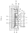
- the main heating section (5) has a panel heater (22), as means of radiant heating for the surface of the printed circuit board (1), and means for hot air heating (23), for blowing hot air locally and roughly perpendicular to the points to be connected on the surface of this printed circuit board (1).
- Means for hot air heating (23) is equipped with hot air header (25), forming a flat space (24) and touching the lower surface of the panel heater (22); a mask plate (26), placed on a surface of this hot air header (25) opposite the printed circuit board (1), wherein blow holes (27), corresponding to the points to be connected are formed, and on which a black body paint coating is made; and a hot air supply duct (28), to supply hot air within the hot air header from one side thereof.
- a dispersion plate (30), on which a plurality of through air holes (29) is dispersed, is placed with space between itself and the mask plate (26).
- Hot air is supplied from the hot air supply duct (28) to between the dispersion plate (30) and the panel heater (22).
- Hot air sources such as the hot air heater (35) and the hot air ventilation fan (36) pass through the hot air supply duct (28) as shown in Figure 5.
- a hot air nozzle tube (31) to blow hot air uniformly from its entire length, is placed inside the hot air supply duct (28).
- the hot air supply duct (28) is placed on one side of the hot air header (25), but the present invention is not limited to that.
- the constitution may also be such that a hot air supply duct (33) is placed so as to surround the periphery of the hot air header (25) and a rectangular, annular hot air nozzle tube (34) is placed therein to send hot air from the hot air source to the right place.
- a hot air supply duct (33) is placed so as to surround the periphery of the hot air header (25) and a rectangular, annular hot air nozzle tube (34) is placed therein to send hot air from the hot air source to the right place.
- a section with small holes (37) for local cooling, in which small holes to blow cool air are installed, and a board support element (38), to support the printed circuit board (1), are placed in the cooling device (12).
- the section with small holes (37) may be constituted with a flat plate (40) in which holes (39) are made, or may have a structure with nozzles (41), conforming to the height of the printed circuit board (1), mounted on a plate (42) for blowing cool air from holes (39) in the nozzles (41), as shown in Figure 7 (c) and (d).
- the distance from the nozzles (41) to the cooled sections of the printed circuit board (1) may be adjusted.
- blow holes may be made in a metal or resin block and the cool air blowing distance, corresponding to the height of the insert mount components (3), may also be adjusted by the carving of the block.
- a fan (45) to ventilate the lower surface of the board with some of the air stream by the wind direction plate (44), may also be installed in the cooling section where the cooling device (12) is installed.
- an isolation plate (32) is installed at a position where it surrounds the periphery of that printed circuit board (1) when the raising and lowering cylinder (11) has raised the printed circuit board (1) to a prescribed heating position.
- This isolation plate (32) prevents the intermixing of the heating atmosphere for the upper section of the printed circuit board (1) and the cooling atmosphere from the cool air, as shown by the broken arrow (C) from means for cooling (12) in the lower section.
- means for pushing boards (9) is constituted of a chain (46), a driving motor (47), and a lever (48) affixed to the chain (46).
- the conveyor (7) transports the printed circuit board (1), on which surface mount components (2) and insert mount components (3) are present together, at a certain speed into the preheating section (4).
- the entire upper surface of the printed circuit board (1) is heated to a temperature in the vicinity of 150°C with the radiant heat from the panel heater (20) and the side flow hot air stream.
- the load on the hot air heater (17) is reduced because the hot air of a certain temperature is recirculated, while regularizing the temperature of the atmosphere within the preheating section (4).
- the temperature of the body sections of the insert mount components (3), which are transported in a position on the lower surface of the printed circuit board (1), is increased by the conduction of heat from the lead sections on the upper surface of the printed circuit board (1).
- the printed circuit board (1) reaches the terminus of the conveyor (7) where means for pushing boards (9) pushes the rear end of the printed circuit board (1) and smoothly transfers the printed circuit board (1) to the conveyor (8).
- Means for pushing boards (9) is established in this way because it is necessary to transport the printed circuit board rapidly; the conveyor (7) is moved at a speed of 0.8 m/min, for example, because the printed circuit board (1) is heated while it is transported continuously through the preheating section (4), through which the conveyor (7) runs, but the printed circuit board (1) is stopped at a prescribed position with the board stopper (10), raised to a prescribed heating position by the raising and lowering cylinder (11), and is heated in the main heating section (5), in which a separate conveyor (8) is operating.
- the printed circuit board (1) transported into the main heating section (5), is stopped at a prescribed position with the board stopper (10) and the conveyor (8) is also stopped. Then means for cooling (12) is raised by the raising and lowering cylinder (11) and the printed circuit board (1), which is supported on the upper end thereof, is raised to a prescribed heating position surrounded by the isolation plate (32).
- the upper surface of the printed circuit board (1) is heated through the heat header (25) with the radiant heat from the panel heater (22).
- hot air is blown from the blow holes (27) of the mask plate (26), in means for hot air heating (23), locally and roughly perpendicular to the points to be connected of the surface mount components (2) and the lead sections, etc., of the insert mount components (3). Consequently, the points to be connected only can be heated quickly and with good precision to the prescribed temperature with hot air of a temperature which does not exceed the temperature of heat resistance of the surface mount components.
- the solder cream of the points to be connected melts and reflow soldering is performed.
- the insert mounted components (3) positioned on the lower surface of the printed circuit board (1), are cooled with the section with small holes (37) for local cooling, in which holes (39) to blow cool air are installed corresponding to the position of the insert mounted components (3).
- the temperature T X of the point to be connected X in the lead of the QFP (2A), as one example of a surface mount component (2), and the temperature T Y of the point to be connected Y in the lead of the aluminum electrolytic capacitor (3A), as one example of an insert mount component (3) are 200°C or greater.
- the solder cream of the points to be connected melts satisfactorily and reflow soldering is performed with certainty.
- the temperature T Z of the body section Z of the aluminum electrolytic capacitor (3A) becomes 160°C or less and heat damage to the aluminum electrolytic capacitor (3A) can be prevented with certainty.
- the mask plate (26) is installed between the panel heater (22) and the printed circuit board (1), the supply of radiant thermal energy to surface mount components (2), which are not subject to cooling, can be isolated and the temperature increase can be controlled.
- the isolation plate (32) can also prevent the intermixing of the cooling atmosphere and the heating atmosphere of the main heating section (5).
- the printed circuit board (1) is lowered to the position of the conveyor (8) once more and the level of the cooling device (12) is dropped below that.
- the cooling device (12) is lowered and the heating of the cooling device (12) itself by the radiant heat is suppressed by its separation of the panel heater (22).
- the cooling device (12) begins to drop, the cooling of the insert mount components (3) is insufficient.
- the lower surface of the printed circuit board (1) is ventilated with some air from the fan (45) by the wind direction plate (44).
- the wind direction plate (44) is set horizontally and the cooling device (12) is cooled with wind from the fan (45).
- the printed circuit board (1) is transported from the main heating section (5) with the conveyor (8) and is cooled with the cooling fans (14) and (15). Then the printed circuit board (1) transfers to the exit conveyor section (6) from the conveyor (8) and is transported to the exit of the reflow device.
Landscapes
- Engineering & Computer Science (AREA)
- Mechanical Engineering (AREA)
- Manufacturing & Machinery (AREA)
- Microelectronics & Electronic Packaging (AREA)
- Electric Connection Of Electric Components To Printed Circuits (AREA)
Priority Applications (1)
| Application Number | Priority Date | Filing Date | Title |
|---|---|---|---|
| EP99115835A EP0960681B1 (de) | 1996-04-16 | 1997-04-15 | Verfahren und Vorrichtung zum Aufschmeltzlöten |
Applications Claiming Priority (6)
| Application Number | Priority Date | Filing Date | Title |
|---|---|---|---|
| JP93710/96 | 1996-04-16 | ||
| JP9371096 | 1996-04-16 | ||
| JP8093710A JPH09283913A (ja) | 1996-04-16 | 1996-04-16 | リフロー方法およびリフロー装置 |
| JP20673596 | 1996-08-06 | ||
| JP8206735A JPH1051130A (ja) | 1996-08-06 | 1996-08-06 | リフロー方法及び装置 |
| JP206735/96 | 1996-08-06 |
Related Child Applications (1)
| Application Number | Title | Priority Date | Filing Date |
|---|---|---|---|
| EP99115835A Division EP0960681B1 (de) | 1996-04-16 | 1997-04-15 | Verfahren und Vorrichtung zum Aufschmeltzlöten |
Publications (2)
| Publication Number | Publication Date |
|---|---|
| EP0802010A1 true EP0802010A1 (de) | 1997-10-22 |
| EP0802010B1 EP0802010B1 (de) | 2001-12-19 |
Family
ID=26435009
Family Applications (2)
| Application Number | Title | Priority Date | Filing Date |
|---|---|---|---|
| EP99115835A Expired - Lifetime EP0960681B1 (de) | 1996-04-16 | 1997-04-15 | Verfahren und Vorrichtung zum Aufschmeltzlöten |
| EP97106166A Expired - Lifetime EP0802010B1 (de) | 1996-04-16 | 1997-04-15 | Verfahren und Vorrichtung zum Reflowlöten |
Family Applications Before (1)
| Application Number | Title | Priority Date | Filing Date |
|---|---|---|---|
| EP99115835A Expired - Lifetime EP0960681B1 (de) | 1996-04-16 | 1997-04-15 | Verfahren und Vorrichtung zum Aufschmeltzlöten |
Country Status (4)
| Country | Link |
|---|---|
| US (3) | US6145734A (de) |
| EP (2) | EP0960681B1 (de) |
| KR (2) | KR100571873B1 (de) |
| DE (2) | DE69723311T2 (de) |
Cited By (5)
| Publication number | Priority date | Publication date | Assignee | Title |
|---|---|---|---|---|
| WO2003079743A3 (de) * | 2002-03-15 | 2003-12-24 | Endress & Hauser Gmbh & Co Kg | Verfahren zum bestücken und löten einer leiterplatte, reflowofen und leiterplatte für ein solches verfahren |
| US6768083B2 (en) * | 2002-09-19 | 2004-07-27 | Speedline Technologies, Inc. | Reflow soldering apparatus and method for selective infrared heating |
| EP1195218A3 (de) * | 2000-10-05 | 2005-12-28 | Minebea Co., Ltd. | Leiterplattenkühlvorrichtung mit Luftleitblechen |
| WO2009120414A1 (en) * | 2008-03-28 | 2009-10-01 | Illinois Tool Works Inc. | Reflow solder oven with cooling diffuser |
| WO2016169551A1 (de) * | 2015-04-24 | 2016-10-27 | Semikron Elektronik Gmbh & Co. Kg | Vorrichtung, verfahren und anlage zur der inhomogenen abkühlung eines flächigen gegenstandes |
Families Citing this family (27)
| Publication number | Priority date | Publication date | Assignee | Title |
|---|---|---|---|---|
| US6367677B1 (en) * | 1999-09-28 | 2002-04-09 | Hill-Rom Services, Inc. | Wave solder apparatus and method |
| JP2001144428A (ja) * | 1999-11-10 | 2001-05-25 | Sony Corp | ハンダ付け装置及びハンダ付け方法 |
| US6347734B1 (en) * | 2000-03-27 | 2002-02-19 | Emc Corporation | Methods and apparatus for installing a module on a circuit board using heating and cooling techniques |
| GB2372228B (en) * | 2000-10-03 | 2004-07-21 | Visteon Global Tech Inc | System and method for mounting electronic components onto flexible substrates |
| DE10194457B4 (de) * | 2000-10-03 | 2006-08-24 | Visteon Global Technologies, Inc., Dearborn | System und Verfahren zum Anbringen elektronischer Komponenten auf flexiblen Substraten |
| DE10133217A1 (de) * | 2001-07-09 | 2003-01-23 | Seho Systemtechnik Gmbh | Verfahren und Vorrichtung zum Verlöten von elektrischen Bauteilen auf Kunststofffolie |
| US20040050915A1 (en) * | 2001-10-03 | 2004-03-18 | Goenka Lakhi Nandlal | System and method for mounting electronic components onto flexible substrates |
| US6642485B2 (en) | 2001-12-03 | 2003-11-04 | Visteon Global Technologies, Inc. | System and method for mounting electronic components onto flexible substrates |
| JP3770238B2 (ja) * | 2002-03-22 | 2006-04-26 | セイコーエプソン株式会社 | 電子デバイス製造装置および電子デバイスの製造方法 |
| US20040211815A1 (en) * | 2003-04-23 | 2004-10-28 | Jackson Hsieh | Apparatus for removing an image sensor from a printed circuit board |
| US7026582B2 (en) * | 2003-05-07 | 2006-04-11 | Visteon Global Technologies, Inc. | Vector transient reflow of lead free solder for controlling substrate warpage |
| WO2006087820A1 (ja) * | 2005-02-21 | 2006-08-24 | Fujitsu Limited | リフロー装置およびリフロー方法 |
| KR200396256Y1 (ko) * | 2005-06-30 | 2005-09-20 | 주식회사 티에스엠 | 리플로우 납땜장치 |
| DE102005032135A1 (de) * | 2005-07-07 | 2007-01-18 | Endress + Hauser Gmbh + Co. Kg | Verfahren zum Löten einer Leiterplatte mit bleifreier Lotpaste in einem Reflow-Lötofen, Leiterplatte für solch ein Verfahren und Reflow-Lötofen |
| DE102005039829A1 (de) * | 2005-08-22 | 2007-03-08 | Endress + Hauser Gmbh + Co. Kg | Verfahren zum Löten von SMD-Bauteilen, Leiterplatte und Reflow-Lötofen dazu |
| DE102008021240B4 (de) * | 2008-04-28 | 2012-11-22 | Ersa Gmbh | Vorrichtung zur thermischen Behandlung von Werkstücken und Verfahren zur Bestimmung der thermischen Prozessstabilität in einer solchen Vorrichtung |
| DE102008033225B3 (de) * | 2008-07-15 | 2009-12-17 | Ersa Gmbh | Vorrichtung zur thermischen Behandlung von Werkstücken |
| JP5424201B2 (ja) * | 2009-08-27 | 2014-02-26 | アユミ工業株式会社 | 加熱溶融処理装置および加熱溶融処理方法 |
| US8196799B2 (en) | 2010-06-28 | 2012-06-12 | Illinois Tool Works Inc. | Compression box for reflow oven heating with a pressurizing plate |
| DE102011081606B4 (de) * | 2011-08-26 | 2022-08-04 | Infineon Technologies Ag | Kühlvorrichtung und Lötanlage |
| US8444043B1 (en) | 2012-01-31 | 2013-05-21 | International Business Machines Corporation | Uniform solder reflow fixture |
| US9170051B2 (en) | 2012-04-02 | 2015-10-27 | Illinois Tool Works Inc. | Reflow oven and methods of treating surfaces of the reflow oven |
| US8940099B2 (en) | 2012-04-02 | 2015-01-27 | Illinois Tool Works Inc. | Reflow oven and methods of treating surfaces of the reflow oven |
| US9198300B2 (en) | 2014-01-23 | 2015-11-24 | Illinois Tool Works Inc. | Flux management system and method for a wave solder machine |
| US9161459B2 (en) | 2014-02-25 | 2015-10-13 | Illinois Tool Works Inc. | Pre-heater latch and seal mechanism for wave solder machine and related method |
| US9296056B2 (en) | 2014-07-08 | 2016-03-29 | International Business Machines Corporation | Device for thermal management of surface mount devices during reflow soldering |
| DE102014118523B4 (de) * | 2014-12-12 | 2017-11-23 | Semikron Elektronik Gmbh & Co. Kg | Kühleinrichtung und Verfahren zum Abkühlen von flüssigem Lot zur Herstellung einer Lötverbindung |
Citations (4)
| Publication number | Priority date | Publication date | Assignee | Title |
|---|---|---|---|---|
| JPH02303674A (ja) * | 1989-05-16 | 1990-12-17 | Matsushita Electric Ind Co Ltd | 加熱方法及びその装置 |
| US5128506A (en) * | 1990-10-30 | 1992-07-07 | Westinghouse Electric Corp. | Method and apparatus for selective infrared soldering using shielding fixtures |
| US5322209A (en) * | 1993-07-19 | 1994-06-21 | General Motors Corporation | Aluminum heat exchanger brazing method and apparatus |
| US5579981A (en) * | 1994-01-13 | 1996-12-03 | Matsushita Electric Industrial Co., Ltd. | Reflow apparatus |
Family Cites Families (23)
| Publication number | Priority date | Publication date | Assignee | Title |
|---|---|---|---|---|
| US3904102A (en) * | 1974-06-05 | 1975-09-09 | Western Electric Co | Apparatus and method for soldering, fusing or brazing |
| US4771929A (en) * | 1987-02-20 | 1988-09-20 | Hollis Automation, Inc. | Focused convection reflow soldering method and apparatus |
| JPH0248132Y2 (de) * | 1988-09-16 | 1990-12-18 | ||
| JP2760057B2 (ja) * | 1989-06-06 | 1998-05-28 | 松下電器産業株式会社 | 部品吸着装置 |
| JPH03114287A (ja) * | 1989-09-28 | 1991-05-15 | Seiko Instr Inc | チップ部品の実装方法 |
| JPH03133198A (ja) * | 1989-10-19 | 1991-06-06 | Fuji Electric Co Ltd | 半田リフロー炉 |
| JPH0756118Y2 (ja) * | 1990-02-20 | 1995-12-25 | 日本アントム工業株式会社 | リフローはんだ付け装置における本加熱ゾーン構造 |
| JP2509373B2 (ja) * | 1990-07-25 | 1996-06-19 | 権士 近藤 | プリント基板のリフロ―はんだ付け方法およびその装置 |
| JP2861324B2 (ja) * | 1990-08-10 | 1999-02-24 | 松下電器産業株式会社 | リフロー設定温度自動決定装置 |
| JPH0739483Y2 (ja) * | 1990-11-15 | 1995-09-13 | 千住金属工業株式会社 | リフロー炉 |
| JPH04200860A (ja) * | 1990-11-29 | 1992-07-21 | Matsushita Electric Ind Co Ltd | リフロー装置および半田付け方法 |
| US5232145A (en) * | 1991-03-29 | 1993-08-03 | Watkins-Johnson Company | Method of soldering in a controlled-convection surface-mount reflow furnace |
| US5195673A (en) * | 1991-09-25 | 1993-03-23 | General Motors Corporation | Method and apparatus for convection brazing of aluminum heat exchangers |
| DE4234855B4 (de) * | 1991-10-18 | 2005-02-24 | Denso Corp., Kariya | Aluminiumhartlötverfahren und Ofen dafür |
| JPH05161961A (ja) * | 1991-11-14 | 1993-06-29 | Tamura Seisakusho Co Ltd | リフロー炉 |
| JP3109689B2 (ja) * | 1992-02-21 | 2000-11-20 | ソニー株式会社 | リフロー半田装置 |
| JPH0773790A (ja) | 1993-07-07 | 1995-03-17 | Komatsu Raito Seisakusho:Kk | 自動販売機の商品等選択スイッチ装置 |
| DE4422341C2 (de) * | 1994-06-27 | 1997-03-06 | Martin Umwelt & Energietech | Löteinrichtung |
| KR100218108B1 (ko) * | 1996-07-22 | 1999-09-01 | 윤종용 | 부품 실장용 리플로우 로 |
| US5971249A (en) * | 1997-02-24 | 1999-10-26 | Quad Systems Corporation | Method and apparatus for controlling a time/temperature profile inside of a reflow oven |
| JP2924888B2 (ja) * | 1997-05-08 | 1999-07-26 | 松下電器産業株式会社 | 電子ユニットの半田付け装置 |
| US5993500A (en) * | 1997-10-16 | 1999-11-30 | Speedline Technololies, Inc. | Flux management system |
| NL1009214C2 (nl) * | 1998-05-19 | 1999-12-07 | Soltec Bv | Reflowoven. |
-
1997
- 1997-04-11 US US08/835,989 patent/US6145734A/en not_active Expired - Fee Related
- 1997-04-15 KR KR1019970013810A patent/KR100571873B1/ko not_active Expired - Fee Related
- 1997-04-15 DE DE69723311T patent/DE69723311T2/de not_active Expired - Fee Related
- 1997-04-15 DE DE69709221T patent/DE69709221T2/de not_active Expired - Fee Related
- 1997-04-15 EP EP99115835A patent/EP0960681B1/de not_active Expired - Lifetime
- 1997-04-15 EP EP97106166A patent/EP0802010B1/de not_active Expired - Lifetime
-
2000
- 2000-08-04 US US09/633,293 patent/US6402011B1/en not_active Expired - Fee Related
-
2002
- 2002-01-04 US US10/035,443 patent/US20020053588A1/en not_active Abandoned
-
2004
- 2004-10-28 KR KR1020040086616A patent/KR100524841B1/ko not_active Expired - Fee Related
Patent Citations (4)
| Publication number | Priority date | Publication date | Assignee | Title |
|---|---|---|---|---|
| JPH02303674A (ja) * | 1989-05-16 | 1990-12-17 | Matsushita Electric Ind Co Ltd | 加熱方法及びその装置 |
| US5128506A (en) * | 1990-10-30 | 1992-07-07 | Westinghouse Electric Corp. | Method and apparatus for selective infrared soldering using shielding fixtures |
| US5322209A (en) * | 1993-07-19 | 1994-06-21 | General Motors Corporation | Aluminum heat exchanger brazing method and apparatus |
| US5579981A (en) * | 1994-01-13 | 1996-12-03 | Matsushita Electric Industrial Co., Ltd. | Reflow apparatus |
Non-Patent Citations (1)
| Title |
|---|
| PATENT ABSTRACTS OF JAPAN vol. 15, no. 85 (M - 1087) 27 February 1991 (1991-02-27) * |
Cited By (12)
| Publication number | Priority date | Publication date | Assignee | Title |
|---|---|---|---|---|
| EP1195218A3 (de) * | 2000-10-05 | 2005-12-28 | Minebea Co., Ltd. | Leiterplattenkühlvorrichtung mit Luftleitblechen |
| WO2003079743A3 (de) * | 2002-03-15 | 2003-12-24 | Endress & Hauser Gmbh & Co Kg | Verfahren zum bestücken und löten einer leiterplatte, reflowofen und leiterplatte für ein solches verfahren |
| DE10211647B4 (de) * | 2002-03-15 | 2014-02-13 | Endress + Hauser Gmbh + Co. Kg | Verfahren zum Bestücken und Löten einer Leiterplatte |
| US6768083B2 (en) * | 2002-09-19 | 2004-07-27 | Speedline Technologies, Inc. | Reflow soldering apparatus and method for selective infrared heating |
| WO2009120414A1 (en) * | 2008-03-28 | 2009-10-01 | Illinois Tool Works Inc. | Reflow solder oven with cooling diffuser |
| US7708183B2 (en) | 2008-03-28 | 2010-05-04 | Illinois Tool Works Inc. | Reflow solder oven with cooling diffuser |
| CN103394782A (zh) * | 2008-03-28 | 2013-11-20 | 伊利诺斯工具制品有限公司 | 具有冷却扩散器的回流焊炉 |
| CN102026768B (zh) * | 2008-03-28 | 2014-05-07 | 伊利诺斯工具制品有限公司 | 具有冷却扩散器的回流焊炉 |
| CN103394782B (zh) * | 2008-03-28 | 2016-08-10 | 伊利诺斯工具制品有限公司 | 具有冷却扩散器的回流焊炉 |
| WO2016169551A1 (de) * | 2015-04-24 | 2016-10-27 | Semikron Elektronik Gmbh & Co. Kg | Vorrichtung, verfahren und anlage zur der inhomogenen abkühlung eines flächigen gegenstandes |
| CN107980014A (zh) * | 2015-04-24 | 2018-05-01 | 赛米控电子股份有限公司 | 用于对平面物体进行非均匀地冷却的装置、方法和系统 |
| US10391572B2 (en) | 2015-04-24 | 2019-08-27 | SEMIKRON ELEKTRONIK GbmH & CO. KG | Device, method, and system for cooling a flat object in a nonhomogeneous manner |
Also Published As
| Publication number | Publication date |
|---|---|
| EP0960681A1 (de) | 1999-12-01 |
| EP0960681B1 (de) | 2003-07-02 |
| US20020053588A1 (en) | 2002-05-09 |
| US6145734A (en) | 2000-11-14 |
| DE69709221D1 (de) | 2002-01-31 |
| EP0802010B1 (de) | 2001-12-19 |
| DE69709221T2 (de) | 2002-06-13 |
| KR19980018079A (ko) | 1998-06-05 |
| US6402011B1 (en) | 2002-06-11 |
| DE69723311D1 (de) | 2003-08-07 |
| KR100524841B1 (ko) | 2005-10-28 |
| DE69723311T2 (de) | 2004-02-12 |
| KR100571873B1 (ko) | 2006-08-03 |
Similar Documents
| Publication | Publication Date | Title |
|---|---|---|
| US6145734A (en) | Reflow method and reflow device | |
| CN103100776B (zh) | 回流焊接系统 | |
| US5154338A (en) | Solder reflow furnace | |
| EP0469788B1 (de) | Verfahren und Vorrichtung für den Rückfluss von gedruckten Schaltungen | |
| JP4043694B2 (ja) | リフロー装置 | |
| JPH1093232A (ja) | リフローはんだ付け装置 | |
| JP2005079466A (ja) | 冷却機構を備えたリフロー装置及び該リフロー装置を用いたリフロー炉 | |
| KR101204716B1 (ko) | 리플로우 장치 | |
| JP7587958B2 (ja) | 搬送加熱装置 | |
| JPH05161961A (ja) | リフロー炉 | |
| US6499994B1 (en) | Heating apparatus in reflow system | |
| JP2004214553A (ja) | リフロー炉 | |
| JPH09283913A (ja) | リフロー方法およびリフロー装置 | |
| JPH1051133A (ja) | リフロー方法及び装置 | |
| JPH1051130A (ja) | リフロー方法及び装置 | |
| JP4957797B2 (ja) | 加熱炉 | |
| JP2004358542A (ja) | リフロー炉およびリフロー炉の温度制御方法 | |
| JP3818834B2 (ja) | リフローはんだ付け装置 | |
| JPH1098263A (ja) | 半田付け装置および半田付け方法 | |
| WO2024202637A1 (ja) | 搬送加熱装置 | |
| JPH10112583A (ja) | リフローハンダ付け方法およびその装置 | |
| JP2018073902A (ja) | リフロー装置 | |
| JPH1098262A (ja) | リフロー装置 | |
| JP2791158B2 (ja) | 加熱装置 | |
| KR20230065752A (ko) | 솔더링을 위한 적외선 램프 어셈블리 및 이를 포함하는 인쇄회로기판 솔더링 장치 |
Legal Events
| Date | Code | Title | Description |
|---|---|---|---|
| PUAI | Public reference made under article 153(3) epc to a published international application that has entered the european phase |
Free format text: ORIGINAL CODE: 0009012 |
|
| AK | Designated contracting states |
Kind code of ref document: A1 Designated state(s): DE FR GB |
|
| 17P | Request for examination filed |
Effective date: 19980420 |
|
| 17Q | First examination report despatched |
Effective date: 19990416 |
|
| GRAG | Despatch of communication of intention to grant |
Free format text: ORIGINAL CODE: EPIDOS AGRA |
|
| GRAG | Despatch of communication of intention to grant |
Free format text: ORIGINAL CODE: EPIDOS AGRA |
|
| GRAH | Despatch of communication of intention to grant a patent |
Free format text: ORIGINAL CODE: EPIDOS IGRA |
|
| GRAH | Despatch of communication of intention to grant a patent |
Free format text: ORIGINAL CODE: EPIDOS IGRA |
|
| GRAA | (expected) grant |
Free format text: ORIGINAL CODE: 0009210 |
|
| AK | Designated contracting states |
Kind code of ref document: B1 Designated state(s): DE FR GB |
|
| REG | Reference to a national code |
Ref country code: GB Ref legal event code: IF02 |
|
| REF | Corresponds to: |
Ref document number: 69709221 Country of ref document: DE Date of ref document: 20020131 |
|
| ET | Fr: translation filed | ||
| PLBE | No opposition filed within time limit |
Free format text: ORIGINAL CODE: 0009261 |
|
| STAA | Information on the status of an ep patent application or granted ep patent |
Free format text: STATUS: NO OPPOSITION FILED WITHIN TIME LIMIT |
|
| 26N | No opposition filed | ||
| PGFP | Annual fee paid to national office [announced via postgrant information from national office to epo] |
Ref country code: FR Payment date: 20060410 Year of fee payment: 10 |
|
| PGFP | Annual fee paid to national office [announced via postgrant information from national office to epo] |
Ref country code: GB Payment date: 20060412 Year of fee payment: 10 |
|
| PGFP | Annual fee paid to national office [announced via postgrant information from national office to epo] |
Ref country code: DE Payment date: 20060413 Year of fee payment: 10 |
|
| GBPC | Gb: european patent ceased through non-payment of renewal fee |
Effective date: 20070415 |
|
| PG25 | Lapsed in a contracting state [announced via postgrant information from national office to epo] |
Ref country code: DE Free format text: LAPSE BECAUSE OF NON-PAYMENT OF DUE FEES Effective date: 20071101 |
|
| PG25 | Lapsed in a contracting state [announced via postgrant information from national office to epo] |
Ref country code: GB Free format text: LAPSE BECAUSE OF NON-PAYMENT OF DUE FEES Effective date: 20070415 |
|
| PG25 | Lapsed in a contracting state [announced via postgrant information from national office to epo] |
Ref country code: FR Free format text: LAPSE BECAUSE OF NON-PAYMENT OF DUE FEES Effective date: 20070430 |