EP1195218A2 - Leiterplattenkühlvorrichtung mit Luftleitblechen - Google Patents
Leiterplattenkühlvorrichtung mit Luftleitblechen Download PDFInfo
- Publication number
- EP1195218A2 EP1195218A2 EP01810966A EP01810966A EP1195218A2 EP 1195218 A2 EP1195218 A2 EP 1195218A2 EP 01810966 A EP01810966 A EP 01810966A EP 01810966 A EP01810966 A EP 01810966A EP 1195218 A2 EP1195218 A2 EP 1195218A2
- Authority
- EP
- European Patent Office
- Prior art keywords
- cooling
- circuit board
- air guide
- air
- rectifier
- Prior art date
- Legal status (The legal status is an assumption and is not a legal conclusion. Google has not performed a legal analysis and makes no representation as to the accuracy of the status listed.)
- Withdrawn
Links
Images



Classifications
-
- B—PERFORMING OPERATIONS; TRANSPORTING
- B23—MACHINE TOOLS; METAL-WORKING NOT OTHERWISE PROVIDED FOR
- B23K—SOLDERING OR UNSOLDERING; WELDING; CLADDING OR PLATING BY SOLDERING OR WELDING; CUTTING BY APPLYING HEAT LOCALLY, e.g. FLAME CUTTING; WORKING BY LASER BEAM
- B23K3/00—Tools, devices or special appurtenances for soldering, e.g. brazing, or unsoldering, not specially adapted for particular methods
- B23K3/08—Auxiliary devices therefor
- B23K3/085—Cooling, heat sink or heat shielding means
-
- B—PERFORMING OPERATIONS; TRANSPORTING
- B23—MACHINE TOOLS; METAL-WORKING NOT OTHERWISE PROVIDED FOR
- B23K—SOLDERING OR UNSOLDERING; WELDING; CLADDING OR PLATING BY SOLDERING OR WELDING; CUTTING BY APPLYING HEAT LOCALLY, e.g. FLAME CUTTING; WORKING BY LASER BEAM
- B23K1/00—Soldering, e.g. brazing, or unsoldering
- B23K1/008—Soldering within a furnace
-
- F—MECHANICAL ENGINEERING; LIGHTING; HEATING; WEAPONS; BLASTING
- F27—FURNACES; KILNS; OVENS; RETORTS
- F27D—DETAILS OR ACCESSORIES OF FURNACES, KILNS, OVENS OR RETORTS, IN SO FAR AS THEY ARE OF KINDS OCCURRING IN MORE THAN ONE KIND OF FURNACE
- F27D15/00—Handling or treating discharged material; Supports or receiving chambers therefor
- F27D15/02—Cooling
- F27D15/0206—Cooling with means to convey the charge
-
- H—ELECTRICITY
- H05—ELECTRIC TECHNIQUES NOT OTHERWISE PROVIDED FOR
- H05K—PRINTED CIRCUITS; CASINGS OR CONSTRUCTIONAL DETAILS OF ELECTRIC APPARATUS; MANUFACTURE OF ASSEMBLAGES OF ELECTRICAL COMPONENTS
- H05K3/00—Apparatus or processes for manufacturing printed circuits
- H05K3/30—Assembling printed circuits with electric components, e.g. with resistors
- H05K3/32—Assembling printed circuits with electric components, e.g. with resistors electrically connecting electric components or wires to printed circuits
- H05K3/34—Assembling printed circuits with electric components, e.g. with resistors electrically connecting electric components or wires to printed circuits by soldering
- H05K3/3494—Heating processes for reflow soldering
-
- H—ELECTRICITY
- H05—ELECTRIC TECHNIQUES NOT OTHERWISE PROVIDED FOR
- H05K—PRINTED CIRCUITS; CASINGS OR CONSTRUCTIONAL DETAILS OF ELECTRIC APPARATUS; MANUFACTURE OF ASSEMBLAGES OF ELECTRICAL COMPONENTS
- H05K7/00—Constructional details common to different types of electric apparatus
- H05K7/20—Modifications to facilitate cooling, ventilating, or heating
-
- H—ELECTRICITY
- H05—ELECTRIC TECHNIQUES NOT OTHERWISE PROVIDED FOR
- H05K—PRINTED CIRCUITS; CASINGS OR CONSTRUCTIONAL DETAILS OF ELECTRIC APPARATUS; MANUFACTURE OF ASSEMBLAGES OF ELECTRICAL COMPONENTS
- H05K2203/00—Indexing scheme relating to apparatus or processes for manufacturing printed circuits covered by H05K3/00
- H05K2203/08—Treatments involving gases
- H05K2203/081—Blowing of gas, e.g. for cooling or for providing heat during solder reflowing
-
- H—ELECTRICITY
- H05—ELECTRIC TECHNIQUES NOT OTHERWISE PROVIDED FOR
- H05K—PRINTED CIRCUITS; CASINGS OR CONSTRUCTIONAL DETAILS OF ELECTRIC APPARATUS; MANUFACTURE OF ASSEMBLAGES OF ELECTRICAL COMPONENTS
- H05K2203/00—Indexing scheme relating to apparatus or processes for manufacturing printed circuits covered by H05K3/00
- H05K2203/11—Treatments characterised by their effect, e.g. heating, cooling, roughening
- H05K2203/1121—Cooling, e.g. specific areas of a PCB being cooled during reflow soldering
Definitions
- the present invention relates to a circuit board cooling apparatus disposed in a flow soldering apparatus to solder electronic parts or the like on a circuit board and used for cooling the circuit board on which the electronic parts have been soldered.
- molten solder is supplied to a joint between the electronic parts to be soldered and the circuit board, the electronic parts are soldered onto the circuit board, and thereafter a circuit board cooling apparatus disposed in the flow soldering apparatus is actuated to cool a temperature of a soldering face of the circuit board down to a room temperature.
- a heat radiation system by means of a cooling fan or a cooling fin As a cooling method, for example, a heat radiation system by means of a cooling fan or a cooling fin is used.
- the former heat radiation system by means of a cooling fan answers a purpose of rapidly releasing the electronic parts from a heat stress suffered at the time of soldering, in which as shown in Fig. 10, air is blown by a cooling fan 4 against a soldered portion 3 on a soldering face 2 of a circuit board 1 at an exit of a solder bath (not shown) to supplement the effect of natural cooling.
- Chilly air (15 to 20°C) may be auxiliarily blown to speed up a cooling rate.
- a cooling fin 5 of multiple structure as a radiation plate is disposed close to the soldered portion 3 on the circuit board 1 at an exit of a solder bath (not shown) to absorb radiation heat from the circuit board 1 which is warm immediately after soldering, thereby indirectly cooling the circuit board 1.
- a refrigerant contact system in which a coolant 6 is brought in direct contact with the soldered portion 3 on the circuit board 1, as shown in Fig. 12.
- the above-described conventional cooling apparatuses have the purpose of rapidly releasing the electronic parts from a heat stress suffered at the time of soldering, and, depending on cooling conditions after soldering, may invite such problems as lift-off, shrinkage cavities that make filet surface rough, faded gloss of the solder after soldering and deterioration in mechanical strength. And the prior art has not provided improvement to solve the above problems.
- the soldered portion when the soldered portion is rapidly cooled, its organization is closely packed thereby improving mechanical strength. It is supposedly desirable that the rapid cooling of the soldered portion is conducted at a cooling rate of 50°C/sec or higher immediately after soldering.
- Pb-free solder is increasingly replacing Sn-Pb eutectic solder. which has been conventionally employed. Because the Pb-free solder is different in composition from the Sn-Pb eutectic solder and has a melting temperature higher by about 40°C, it is becoming increasingly important to increase the cooling rate for providing a high quality soldering.
- the cooling rate is about 1 to 3°C/sec in case of only blowing air, in which air is blown entirely over the soldering face 2 of the circuit board 1 and therefore the cooling capacity is decentralized making it difficult to set the cooling rate to 50°C/sec or higher, which is not good enough to conduct an excellent soldering.
- the cooling fan 4 shown in Fig. 10 causes a turbulent air flow making it difficult to focus and target air onto a soldered joint surface for cooling.
- the cooling fan 4 cools also a portion to be soldered and a surface of solder in the solder bath which is located close to the soldered portion, as a result of which the quality of joint may be deteriorated.
- the cooling effect is relatively small, and in case of a continuous operation the cool fin 5 cannot keep absorbing heat completely due to its limited radiation capacity and the cooling effect is further deteriorated.
- a cooling method shown in Fig. 12 provides a rapid cooling effect but may lead to such problems that a coolant 6 as a refrigerant accidentally gets into the solder bath which contains molten solder of a high temperature, and that mounted parts are rapidly cooled and destroyed due to a heat stress.
- the present invention has been made under the above-mentioned circumstances, and therefore an object of the present invention is to provide a circuit board cooling apparatus which is capable of cooling a circuit board pinpointing a soldered portion, thereby improving a cooling rate.
- a circuit board cooling apparatus including a cooling compartment having an open top and a bottom with a plurality of openings for taking in air, in which a circuit board to which electronic parts are soldered is conveyed over the open top of the cooling compartment, and a soldered portion on the circuit board is cooled by cooling air taken in through the openings of the cooling compartment, the cooling apparatus comprising:
- a length for which the air guide plate is in contact with a soldering face of the circuit board is set to be 3 cm or smaller but larger than 0 cm.
- the air guide plates are made of polyimide.
- the air guide plates are made of glass cloth impregnated with fluorine resin.
- the air guide plates are coated with an antistatic material.
- the air guide plates are detachably attached to the inclined rectifier plates.
- the cooling compartment is sectioned into a plurality of zones by at least one partition, each of the plurality of zones has each of the openings through which the cooling air passes, and a valve is disposed on each of branch pipes of a blast pipe, which communicate with the respective openings.
- an inclination angle of the inclined rectifier plates is set to 30 to 70°.
- a circuit board cooling apparatus 10 according to a first embodiment of the present invention will be described with reference to Figs. 1 to 5B.
- the same parts as those in Figs. 10 to 12 are designated by identical reference numerals and their description will be appropriately omitted.
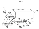
- the circuit board cooling apparatus 10 includes a cooling compartment 11 where a circuit hoard 1 is cooled as shown in Figs. 1 and 2.
- the cooling compartment 11 is substantially rectangular in a plan view and has an open top (cooling compartment top) 12.
- a solder bath (not shown) is disposed close to the cooling compartment 11, and the circuit board 1 soldered at the solder bath is conveyed over the cooling compartment top 12.
- the cooling compartment 11 is designed in such a manner that a dimension in a direction A of conveying the circuit board 1 is about 250 mm and a dimension in a direction B orthogonal to the direction A is about 500 mm.
- a bottom 13 of the cooling compartment 11 (cooling compartment bottom) is so structured as to be inclined downward from both sides 11a and 11b on the direction A side toward an approximate center with regard to the direction A.
- a cooling air intake portion 14 which is substantially box-shaped, projecting downward and extending along the direction B is formed at the approximate center of the cooling compartment bottom 13.
- Aplurality of openings 15 are formed at a bottom 14a of the cooling air intake portion 14 along a longitudinal direction thereof.
- the openings 15 lead eventually to a blast pipe 16.
- the blast pipe 16 comprises a main pipe 17 that guides cooling air that has passed through a cooling device (not shown) and a plurality of branch pipes (three in this embodiment, and hereinafter those pipes are appropriately referred to as first, second and third branch pipes 18a, 18b and 18c in the order from the left in Fig. 2). Distal ends of the first, second and third branch pipes 18a, 18b and 18c are connected with the respective openings 15.
- the first, second and third branch pipes 18a, 18b and 18c are provided with first, second and third valves 19a, 19b and 19c (hereinafter generically referred to as "valves 19"), respectively, so as to control the supply of the cooling air to the openings 15.
- Electronic parts 20 are disposed on one face (an upper side in Fig. 3) of the circuit board 1, and protruding portions (not shown) of the electronic parts pass through holes (not shown) formed in the circuit board 1 and project from an opposite face (a lower side in Fig. 3) so that the electronic parts 20 are soldered to the circuit board 1 on the opposite face of the circuit board 1.
- soldered face 2 the above opposite face of the circuit board 1
- soldered portion 3 a portion of the soldering face 2 which has been soldered as well as solder itself thereon.
- the circuit board 1 is conveyed over the cooling compartment top 12 in the direction A with the soldering face 2 directed toward the cooling compartment bottom 13.
- a plane rectifier plate 21 made of stainless steel or aluminum is disposed in parallel with the circuit board 1 conveyed over the cooling compartment top 12 and is positioned above the openings 15 inside the cooling compartment 11.
- the plane rectifier plate 21 comprises an upper plane rectifier plate 22 and a lower plane rectifier plate 23 which are disposed in parallel with each other with a given gap therebetween.
- a plurality of holes 24 are provided substantially in a matrix manner on the upper plane rectifier plate 22 and the lower plane rectifier plate 23, respectively, so as to pass the cooling air and to rectify its flows, then guide upward.
- the plurality of holes 24 in the upper plane rectifier plate 22 are arranged so as to be shifted from one line to another and from one row to another. Also, the plurality of holes 24 in the lower plane rectifier plate 23 are arranged in the same manner. And, the plurality of holes 24 in the upper plane rectifier plate 22 and the plurality of holes 24 in the lower plane rectifier plate 23 are arranged so as to be shifted from each other vertically (not coincide with each other vertically). With the plurality of holes 24 of the upper and lower plane rectifier plates 22 and 23 arranged as described above, a pressure of the cooling air (air pressure) is uniformed, which allows the cooling air to be satisfactorily guided upward suppressing a turbulent or reverse flow.
- air pressure air pressure
- the arrangement of the holes 24 is not limited to the above-mentioned embodiment.
- a plurality of slits (not shown) that extend in the direction A may be arranged in the direction B orthogonal to the direction A in the upper plane rectifier plate 22 or the lower plane rectifier plate 23, or a plurality of slits that extend in the direction B may be arranged in the direction A.
- a plurality of inclined rectifier plates 25 made of stainless steel or aluminum with an inclination angle of about 45° are fitted onto the upper plane rectifier plate 22 in the direction A so as not to cover the holes 24.
- the inclined rectifier plates 25 are disposed in a plurality of lines (nine in this embodiment) in the direction A as shown in Fig. 3 and in a plurality of rows (three in this embodiment each having four air guide plates 26 (to be described later)) in the direction B as shown in Fig. 1.
- twelve air guide plates 26 at the first (forefront) line, eight at the second line and four at the third line are only shown for convenience, and remaining air guide plates 26 are omitted.
- the inclined rectifier plates 25 allows the cooling air from the plane rectifier plate 21 to be rectified so as to be duly guided upward. In this case, since the inclined rectifier plate 25 has an inclination angle of about 45° with respect to the upper plane rectifier plate 22, the cooling air is surely rectified to flow toward the soldered portion 3.
- the inclination angle of the inclined rectifier plate 25 is not limited to about 45° but may be set in a range of 30 to 70°.
- the reason that the inclination angle of the inclined rectifier plate 25 is set in a range of 30 to 70° is that the following characteristic deteriorations can be prevented which may occur when the inclination angle of the inclined rectifier plate 25 is set to under 30° or over 70°.
- the air guide plate 26 formed of a heat-resistant film, having flexibility and attached to the inclined rectifier plates 25 it is necessary for the air guide plate 26 to receive the air pressure of the cooling air coming from its lower side.
- the air guide plate 26 if the inclination angle of the inclined rectifier plate 25 is set to less than 30°, a distal end 26b of the air guide plate 26 hangs down with its own weight and the effect of blowing the cooling air against circuit board 1 deteriorates.
- the inclination angle of the inclined rectifier plate 25 is set to more than 70°, the air guide plate 26 is pushed too strongly against the circuit board 1 due to the air pressure, thereby disturbing flows of air coming from this side.
- a plurality of protrusions 25a are formed toward a distal end of the inclined rectifier plate 25 at intervals in a longitudinal direction of the inclined rectifier plate 25 as shown in Fig. 5A.
- the air guide plates 26 each have two holes 26a, into which the protrusions 25a are inserted thereby holding the air guide plate 26 detachably to the inclined rectifier plate 25.
- the air guide plate 26 is formed of a heat-resistant film of polyimide, has flexibility, and is shaped substantially rectangular as shown in Figs. 5A and 5B measuring about 100 mm in length and 20 to 30 mm in width with a thickness of 0.1 to 0.2 mm.
- the air guide plate 26 has the holes 26a toward its proximal end, which are slightly smaller in diameter than the protrusions 25a.
- the protrusions 25a are inserted into the holes 26a to thereby hold the air guide plates 26 detachably to the inclined rectifier plate 25.
- the distal end 26b of the air guide plate 26 is adapted to contact for a given length L with the soldering face 2 of the circuit board 1 which has been conveyed over the cooling compartment 11.
- the length L is set to be 3 cm or smaller but larger than 0 cm.
- Partitions 30 are disposed inside the cooling compartment 11 in parallel with the direction A, whereby the cooling compartment 11 is sectioned into a plurality of zones (three in this embodiment, first, second and third zones 31a, 31b and 31c from the upper side in Fig. 1 to the lower side). Selection of zones to be used is made from the first, second and third zones 31a, 31b and 31c according to the size of the circuit board 1, and the valves 19 for the selected zones only are opened, thereby narrowing the usage of the zones down to minimum necessity for efficiently cooling the circuit board 1.
- the circuit board 1 which has been soldered at the solder bath (not shown) disposed close to the cooling compartment 11 is conveyed in the direction A over the cooling compartment top 12.
- the cooling air pushes with its pressure the distal end 26b of the air guide plate 26 against the soldering face 2 (soldered portion 3) of the circuit board 1.
- the length L for which the air guide plate 26 is in contact with the circuit board 1 is set to be 3 cm or smaller but larger than 0 cm as described above, so that the cooling air also flows through between the soldering face 2 and the air guide plate 26 as indicated by an arrow D in Fig. 3 and is converged on the soldered portion 3.
- the soldered portion 3 is pinpointedly cooled and the cooling rate is improved, thereby improving the cooling capability.
- the cooling air is accurately targeted at the soldered portion 3, the surface of solder contained in the solder bath can be prevented from getting undesirably cooled.
- the cooling compartment 11 can be located close to the solder bath, as a result of which the entire apparatus including the cooling compartment 11 and the solder bath can be downsized.
- the air guide plate 26 which has heat resistance, is hard to wear even if it is in direct contact with the soldered portion 3 with a high temperature. As a result, the intake of the cooling air and the maintenance of the excellent cooling rate can be stably performed over a long period of time.
- the cooling rate of 50°C/sec can be obtained as described above, high quality soldering strength can be ensured. Also, because the cooling rate of 50°C/sec or higher is obtained and the high quality soldering strength is ensured as described even in the circuit board 1 in which Pb-free solder is used for soldering the electronic parts 20, the use of the Pb-free solder is promoted replacing Sn-Pb eutectic solder which has been conventionally employed, thereby enhancing environmental protection.
- the air guide plate 26 is detachably attached to the inclined rectifier plate 25, it can be readily replaced by a new one when required to do so, which reduces a loss of time during a production process and improves the productivity.
- the air guide plate 26 is adapted to be in close contact with the soldered portions 3 of various configurations, thereby efficiently applying the cooling air to the soldered portions 3, which improves the cooling capability.
- the air guide plate 26 since the air guide plate 26 has flexibility, the air guide plate 26 is adapted to be in close contact with the soldered portions 3 of various configurations, thereby efficiently applying the cooling air onto the soldered portions 3, which improves the cooling capability.
- the air guide plate 26 is made of a heat-resistant film of polyimide, but may be of glass cloth impregnated with fluorine resin instead.
- the air guide plate 26 can be coated with an antistatic material (not shown) to prevent the static electrification. If the air guide plate 26 is coated with an antistatic material, the apparatus can be used for the circuit board 1 which is provided with the electronic parts 20 unsuitable for the static electrification, and its versatility can be expanded as much.
- the antistatic material is to be made of polypyrrole, and when the air guide plate 26 is made of glass cloth impregnated with fluorine resin, the antistatic material is to be made of carbon, whereby the static electrification can be appropriately prevented.
- the above embodiment employs two plane rectifier plates 21, i.e., upper and lower plane rectifier plates 22 and 23.
- the present invention is not limited to this structure but may employ one plane rectifier plate or three or more plane rectifier plates.
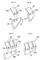
- a multiple air guide plate 26A may be used as shown in Figs. 6A and 6B (second embodiment).
- the multiple air guide plate 26A comprises a plurality of air guide plates proper 26f each corresponding to the air guide plate 26 of the first embodiment and a plurality of plate connecting portions 26g that connect the plurality of air guide plates proper 26f at proximal ends.
- One hole 26a is formed toward the proximal end of the respective air guide plates proper 26f.
- a plurality of protrusions 25a are formed on the respective inclined rectifier plates 25 and positioned corresponding to a plurality of holes 26a of the multiple air guide plate 26A, and the protrusions 25a are inserted into the holes 26a so as to retain the multiple air guide plate 26A as shown in Fig. 6B.
- one multiple air guide plate 26A has a plurality of air guide plates proper 26f (corresponding to the air guide plate 26 in this first embodiment)
- the plurality of air guide plates proper 26f gathered as one multiple air guide plate 26A can be attached to the inclined rectifier plate 25.
- the attachment is rapidly and readily conducted as compared with the first embodiment in which the plurality of air guide plates 26 are attached individually, and thereby the productivity can be improved.
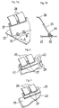
- a plurality of pairs of pressure bar springs 36 each pair aligned in the direction A and having a gap 35 are disposed on the upper plane rectifier plate 22 in the direction B orthogonal to the direction A and welded thereto, as shown in Figs. 7A and 7B.
- the inclined rectifier plate 25 is detachably attached to the upper plane rectifier plate 22 by means of the pressure bar springs 36 and the air guide plate 26 is fixed to the inclined rectifier plate 25 with an adhesive 37 (third embodiment).
- the inclined rectifier plate 25 can be detached from the plane rectifier plate 21 by releasing the pressure of the pressure bar springs 36.
- the replacement of the air guide plate 26 can be readily conducted, whereby the loss of time in the production process can be shortened and the productivity can be improved.
- the air guide plate 26 may be fixed with an adhesive 37 to a support plate 40 which is about 0.5 mm in thickness, and the support plate 40 may be detachably attached to the inclined rectifier plate 25 by screws 41 (fourth embodiment), as shown in Fig. 8.
- the air guide plate 26 can be detached from the inclined rectifier plate 25 together with the support plate 40 by unscrewing the screws 41, the replacement of the air guide plate 26 can be relatively readily conducted, whereby the loss of time in the production process can be shortened and the productivity can be improved as in the second embodiment.
- the support plate 40 may be detachably attached to the inclined rectifier plate 25 with an adhesive 42 (fifth embodiment) as shown in Fig. 9.
- the adhesive 42 breaks up on the inclined rectifier plate 25 by pulling the support plate 40 to detach the air guide plate 26 from the inclined rectifier plate 25 together with the support plate 40, the replacement of the air guide plate 26 can be readily conducted, whereby the loss of time in the production process can be shortened and the productivity can be improved as in the fourth embodiment.
- the cooling air from the openings of the cooling compartment is rectified and guided upward by means of the plane rectifier plates and the inclined rectifier plates, and also flows through between the soldering face of the circuit board and the air guide plate so as to be converged on the soldered portion on the circuit board.
- the soldered portion is pinpointedly cooled and the cooling rate is improved, thereby improving the cooling capability.
- the soldered portion is pinpointedly cooled, such a drawback that the surface of solder in the solder bath disposed close to the cooling compartment is undesirably cooled can be prevented.
- the cooling compartment can be located close to the solder bath, as a result of which the entire apparatus including the cooling compartment and the solder bath can he downsized.
- the air guide plate which has heat resistance, is hard to wear even if it is in direct contact with the soldered portion with a high temperature. As a result, the intake of the cooling air and the maintenance of the excellent cooling rate can be stably performed over a long period of time.
- the air guide plate has flexibility, the air guide plate is adapted to be in close contact with the soldered portions of various configurations, thereby efficiently applying the cooling air to the soldered portions, which improves the cooling capability.
- the air guide plate in contact with the circuit board is set to be 3 cm or smaller but larger than 0 cm, the air guide plate is adapted to be in close contact with the soldered portions of various configurations, thereby efficiently applying the cooling air to the soldered portions, which improves the cooling capability.
- the apparatus since antistatic effect is obtained by the antistatic material coated on the air guide plate, the apparatus can be used for the circuit board provided with the electronic parts apt to be easily affected or damaged by static electrification, and its versatility can be expanded as much.
- the air guide plate since the air guide plate is detachably attached to the inclined rectifier plate, the air guide plate can be readily replaced by a new one, thereby reducing a loss of time during a production process and improving the productivity.
- the cooling compartment is sectioned into a plurality of zones by at least one partition and since valves corresponding to the respective zones can be opened independently so that the cooling air can be taken in only for the zones required to cover the size of the circuit board, the cooling capability can be improved as much.
- the inclination angle of the inclined rectifier plate is 30 to 70°, the cooling air is surely rectified to flow toward the circuit board, and the circuit board is efficiently cooled.
Landscapes
- Engineering & Computer Science (AREA)
- Mechanical Engineering (AREA)
- Microelectronics & Electronic Packaging (AREA)
- Manufacturing & Machinery (AREA)
- Physics & Mathematics (AREA)
- Thermal Sciences (AREA)
- General Engineering & Computer Science (AREA)
- Electric Connection Of Electric Components To Printed Circuits (AREA)
- Cooling Or The Like Of Electrical Apparatus (AREA)
- Molten Solder (AREA)
Applications Claiming Priority (2)
| Application Number | Priority Date | Filing Date | Title |
|---|---|---|---|
| JP2000306194A JP3491199B2 (ja) | 2000-10-05 | 2000-10-05 | 回路基板用冷却装置 |
| JP2000306194 | 2000-10-05 |
Publications (2)
| Publication Number | Publication Date |
|---|---|
| EP1195218A2 true EP1195218A2 (de) | 2002-04-10 |
| EP1195218A3 EP1195218A3 (de) | 2005-12-28 |
Family
ID=18786925
Family Applications (1)
| Application Number | Title | Priority Date | Filing Date |
|---|---|---|---|
| EP01810966A Withdrawn EP1195218A3 (de) | 2000-10-05 | 2001-10-03 | Leiterplattenkühlvorrichtung mit Luftleitblechen |
Country Status (3)
| Country | Link |
|---|---|
| US (1) | US6466440B2 (de) |
| EP (1) | EP1195218A3 (de) |
| JP (1) | JP3491199B2 (de) |
Cited By (1)
| Publication number | Priority date | Publication date | Assignee | Title |
|---|---|---|---|---|
| CN115866913A (zh) * | 2022-12-30 | 2023-03-28 | 益阳市明正宏电子有限公司 | 一种pcb电路板生产运输装置 |
Families Citing this family (15)
| Publication number | Priority date | Publication date | Assignee | Title |
|---|---|---|---|---|
| JP3652634B2 (ja) * | 2001-10-05 | 2005-05-25 | 本田技研工業株式会社 | 高圧電装部品の冷却構造 |
| JP2007502214A (ja) * | 2003-05-13 | 2007-02-08 | ジョンズ ホプキンス ユニバーシティ | 反応性多層フォイルを用いて形成されるナノ構造はんだ付け又はろう付け接合部 |
| US7233493B2 (en) * | 2004-08-10 | 2007-06-19 | E. I. Du Pont De Nemours And Company | Electronic device having a temperature control system including a ductwork assembly |
| CA2703963C (en) * | 2007-10-25 | 2013-12-03 | Nexxus Lighting, Inc. | Apparatus and methods for thermal management of electronic devices |
| US8047271B2 (en) * | 2007-12-20 | 2011-11-01 | Fu Zhun Precision Industry (Shen Zhen) Co., Ltd. | Heat dissipation device having a fan holder |
| WO2011044951A1 (en) * | 2009-10-16 | 2011-04-21 | Dresser Wayne Ab | Electronics module for a fuel dispensing unit |
| CN102541216B (zh) * | 2010-12-11 | 2016-05-04 | 浙江大学城市学院 | 导风罩以及具有该导风罩的计算机系统 |
| CN105718007B (zh) * | 2010-12-11 | 2018-11-30 | 李驹光 | 一种计算机系统 |
| JP6003756B2 (ja) * | 2013-03-26 | 2016-10-05 | 富士ゼロックス株式会社 | 送風装置及び画像形成装置 |
| JP2015137889A (ja) * | 2014-01-21 | 2015-07-30 | 三菱電機株式会社 | 制御基板のテスト方法 |
| US9717169B2 (en) * | 2015-09-28 | 2017-07-25 | Lenovo Enterprise Solutions (Singapore) Pte. Ltd. | Mitigating electromagnetic interference in a computing device |
| US20170099746A1 (en) * | 2015-10-01 | 2017-04-06 | Microsoft Technology Licensing, Llc | Layered airflow cooling for electronic components |
| CN107087347B (zh) * | 2017-06-20 | 2023-10-10 | 昆山市华新电路板有限公司 | Pcb板用冷却治具 |
| CN112272473A (zh) * | 2020-10-28 | 2021-01-26 | 江西舜曙照明电器有限公司 | 用于led电源的铝合金防水外壳 |
| KR102899407B1 (ko) | 2022-06-13 | 2025-12-12 | 센주긴조쿠고교 가부시키가이샤 | 분류 납땜 장치 |
Family Cites Families (10)
| Publication number | Priority date | Publication date | Assignee | Title |
|---|---|---|---|---|
| US5183104A (en) * | 1989-06-16 | 1993-02-02 | Digital Equipment Corporation | Closed-cycle expansion-valve impingement cooling system |
| US5428503A (en) * | 1992-03-24 | 1995-06-27 | Hitachi, Ltd. | Jet cooling apparatus for cooling electronic equipment and computer having the same mounted thereon |
| US5567151A (en) * | 1994-10-21 | 1996-10-22 | Senju Metal Industry Company Limited | Reflow furnaces with hot air blow type heaters |
| US6145734A (en) * | 1996-04-16 | 2000-11-14 | Matsushita Electric Industrial Co., Ltd. | Reflow method and reflow device |
| US5814789A (en) * | 1996-07-18 | 1998-09-29 | Btu International, Inc. | Forced convection furnance gas plenum |
| DE19733134C2 (de) * | 1997-07-31 | 2001-10-11 | Knuerr Mechanik Ag | Anordnung zur Belüftung von elektrischen und elektronischen Geräten und Baugruppen und Verfahren zur Herstellung der Anordnung |
| NL1009214C2 (nl) * | 1998-05-19 | 1999-12-07 | Soltec Bv | Reflowoven. |
| US6181557B1 (en) * | 1999-10-29 | 2001-01-30 | Motorola, Inc. | Electronic component, method of cooling, and damper therefor |
| US6347734B1 (en) * | 2000-03-27 | 2002-02-19 | Emc Corporation | Methods and apparatus for installing a module on a circuit board using heating and cooling techniques |
| US6272311B1 (en) * | 2000-10-12 | 2001-08-07 | Heidelberg Digital L.L.C. | Air cooling station for electrophotographic copier |
-
2000
- 2000-10-05 JP JP2000306194A patent/JP3491199B2/ja not_active Expired - Fee Related
-
2001
- 2001-10-03 US US09/968,759 patent/US6466440B2/en not_active Expired - Fee Related
- 2001-10-03 EP EP01810966A patent/EP1195218A3/de not_active Withdrawn
Cited By (1)
| Publication number | Priority date | Publication date | Assignee | Title |
|---|---|---|---|---|
| CN115866913A (zh) * | 2022-12-30 | 2023-03-28 | 益阳市明正宏电子有限公司 | 一种pcb电路板生产运输装置 |
Also Published As
| Publication number | Publication date |
|---|---|
| JP3491199B2 (ja) | 2004-01-26 |
| US20020041485A1 (en) | 2002-04-11 |
| US6466440B2 (en) | 2002-10-15 |
| JP2002118353A (ja) | 2002-04-19 |
| EP1195218A3 (de) | 2005-12-28 |
Similar Documents
| Publication | Publication Date | Title |
|---|---|---|
| US6466440B2 (en) | Circuit board cooling apparatus with air guide plates | |
| US8599557B2 (en) | Printed circuit board cooling assembly | |
| US5785233A (en) | Apparatus and method for solder reflow bottom cooling | |
| JP2009148817A (ja) | リフロー装置 | |
| CA1143863A (en) | Device for cooling freshly-soldered circuit boards | |
| US5593499A (en) | Dual air knife for hot air solder levelling | |
| CN1188022C (zh) | 电子装置的制造设备和制造方法 | |
| US20040124845A1 (en) | Device for compensating for heat deviation in a modular IC test handler | |
| KR20210015957A (ko) | 열교환기, 열교환기 유닛, 및 냉동 사이클 장치 | |
| JP2003223092A (ja) | 画像形成装置の用紙冷却装置 | |
| JP2011110568A (ja) | 伝熱管の溶接用冷却装置 | |
| US7434421B2 (en) | Fiberizing apparatus | |
| JP2003332725A (ja) | リフロー加熱方法およびリフロー加熱装置 | |
| JP2020136626A (ja) | はんだ付け装置及びはんだ付け装置にパッキンを固定する方法 | |
| JP2013027931A (ja) | リフロー装置 | |
| JP2000188464A (ja) | 自動はんだ付け装置 | |
| KR100494932B1 (ko) | 냉각지그가 구비된 레이져 브레이징 장치 | |
| CN109465612A (zh) | 焊接式铜散热器制作工艺 | |
| JP2003294799A (ja) | 環境試験装置 | |
| KR102702822B1 (ko) | Pcb 냉각장치 및 그 제조방법 | |
| KR20180027284A (ko) | 복수 열전소자용 소형냉각장치 | |
| CN216698304U (zh) | 半导体焊接保护治具 | |
| KR20080019087A (ko) | 리플로우 솔더링머신 | |
| JPH07336040A (ja) | はんだ付け基板の冷却装置 | |
| CN216607549U (zh) | 一种电路板回流焊装置 |
Legal Events
| Date | Code | Title | Description |
|---|---|---|---|
| PUAI | Public reference made under article 153(3) epc to a published international application that has entered the european phase |
Free format text: ORIGINAL CODE: 0009012 |
|
| AK | Designated contracting states |
Kind code of ref document: A2 Designated state(s): AT BE CH CY DE DK ES FI FR GB GR IE IT LI LU MC NL PT SE TR |
|
| AX | Request for extension of the european patent |
Free format text: AL;LT;LV;MK;RO;SI |
|
| PUAL | Search report despatched |
Free format text: ORIGINAL CODE: 0009013 |
|
| AK | Designated contracting states |
Kind code of ref document: A3 Designated state(s): AT BE CH CY DE DK ES FI FR GB GR IE IT LI LU MC NL PT SE TR |
|
| AX | Request for extension of the european patent |
Extension state: AL LT LV MK RO SI |
|
| RIC1 | Information provided on ipc code assigned before grant |
Ipc: 7F 27B 9/10 B Ipc: 7H 05K 3/34 B Ipc: 7H 05K 7/20 B Ipc: 7B 23K 3/06 A |
|
| 17P | Request for examination filed |
Effective date: 20060221 |
|
| RTI1 | Title (correction) |
Free format text: CIRCUIT BOARD COOLING APPARATUS WITH AIR GUIDE PLATES |
|
| AKX | Designation fees paid |
Designated state(s): DE FR GB |
|
| STAA | Information on the status of an ep patent application or granted ep patent |
Free format text: STATUS: THE APPLICATION HAS BEEN WITHDRAWN |
|
| 18W | Application withdrawn |
Effective date: 20080916 |