EP0776026B1 - Gerät zur Herstellung einer Halbleitervorrichtung mit Vakuumsystem - Google Patents
Gerät zur Herstellung einer Halbleitervorrichtung mit Vakuumsystem Download PDFInfo
- Publication number
- EP0776026B1 EP0776026B1 EP96304288A EP96304288A EP0776026B1 EP 0776026 B1 EP0776026 B1 EP 0776026B1 EP 96304288 A EP96304288 A EP 96304288A EP 96304288 A EP96304288 A EP 96304288A EP 0776026 B1 EP0776026 B1 EP 0776026B1
- Authority
- EP
- European Patent Office
- Prior art keywords
- venting
- load lock
- semiconductor device
- manufacturing apparatus
- device manufacturing
- Prior art date
- Legal status (The legal status is an assumption and is not a legal conclusion. Google has not performed a legal analysis and makes no representation as to the accuracy of the status listed.)
- Expired - Lifetime
Links
Images

Classifications
-
- H—ELECTRICITY
- H10—SEMICONDUCTOR DEVICES; ELECTRIC SOLID-STATE DEVICES NOT OTHERWISE PROVIDED FOR
- H10D—INORGANIC ELECTRIC SEMICONDUCTOR DEVICES
- H10D48/00—Individual devices not covered by groups H10D1/00 - H10D44/00
- H10D48/01—Manufacture or treatment
- H10D48/04—Manufacture or treatment of devices having bodies comprising selenium or tellurium in uncombined form
- H10D48/042—Preparation of foundation plates
-
- H—ELECTRICITY
- H10—SEMICONDUCTOR DEVICES; ELECTRIC SOLID-STATE DEVICES NOT OTHERWISE PROVIDED FOR
- H10P—GENERIC PROCESSES OR APPARATUS FOR THE MANUFACTURE OR TREATMENT OF DEVICES COVERED BY CLASS H10
- H10P72/00—Handling or holding of wafers, substrates or devices during manufacture or treatment thereof
- H10P72/30—Handling or holding of wafers, substrates or devices during manufacture or treatment thereof for conveying, e.g. between different workstations
- H10P72/33—Handling or holding of wafers, substrates or devices during manufacture or treatment thereof for conveying, e.g. between different workstations into and out of processing chamber
- H10P72/3306—Horizontal transfer of a single workpiece
-
- C—CHEMISTRY; METALLURGY
- C23—COATING METALLIC MATERIAL; COATING MATERIAL WITH METALLIC MATERIAL; CHEMICAL SURFACE TREATMENT; DIFFUSION TREATMENT OF METALLIC MATERIAL; COATING BY VACUUM EVAPORATION, BY SPUTTERING, BY ION IMPLANTATION OR BY CHEMICAL VAPOUR DEPOSITION, IN GENERAL; INHIBITING CORROSION OF METALLIC MATERIAL OR INCRUSTATION IN GENERAL
- C23C—COATING METALLIC MATERIAL; COATING MATERIAL WITH METALLIC MATERIAL; SURFACE TREATMENT OF METALLIC MATERIAL BY DIFFUSION INTO THE SURFACE, BY CHEMICAL CONVERSION OR SUBSTITUTION; COATING BY VACUUM EVAPORATION, BY SPUTTERING, BY ION IMPLANTATION OR BY CHEMICAL VAPOUR DEPOSITION, IN GENERAL
- C23C14/00—Coating by vacuum evaporation, by sputtering or by ion implantation of the coating forming material
- C23C14/22—Coating by vacuum evaporation, by sputtering or by ion implantation of the coating forming material characterised by the process of coating
- C23C14/56—Apparatus specially adapted for continuous coating; Arrangements for maintaining the vacuum, e.g. vacuum locks
- C23C14/564—Means for minimising impurities in the coating chamber such as dust, moisture, residual gases
- C23C14/566—Means for minimising impurities in the coating chamber such as dust, moisture, residual gases using a load-lock chamber
-
- H—ELECTRICITY
- H01—ELECTRIC ELEMENTS
- H01J—ELECTRIC DISCHARGE TUBES OR DISCHARGE LAMPS
- H01J37/00—Discharge tubes with provision for introducing objects or material to be exposed to the discharge, e.g. for the purpose of examination or processing thereof
- H01J37/02—Details
- H01J37/18—Vacuum locks ; Means for obtaining or maintaining the desired pressure within the vessel
-
- H—ELECTRICITY
- H01—ELECTRIC ELEMENTS
- H01J—ELECTRIC DISCHARGE TUBES OR DISCHARGE LAMPS
- H01J37/00—Discharge tubes with provision for introducing objects or material to be exposed to the discharge, e.g. for the purpose of examination or processing thereof
- H01J37/32—Gas-filled discharge tubes
- H01J37/32431—Constructional details of the reactor
- H01J37/3244—Gas supply means
-
- H—ELECTRICITY
- H01—ELECTRIC ELEMENTS
- H01J—ELECTRIC DISCHARGE TUBES OR DISCHARGE LAMPS
- H01J37/00—Discharge tubes with provision for introducing objects or material to be exposed to the discharge, e.g. for the purpose of examination or processing thereof
- H01J37/32—Gas-filled discharge tubes
- H01J37/32431—Constructional details of the reactor
- H01J37/32733—Means for moving the material to be treated
- H01J37/32743—Means for moving the material to be treated for introducing the material into processing chamber
-
- H—ELECTRICITY
- H10—SEMICONDUCTOR DEVICES; ELECTRIC SOLID-STATE DEVICES NOT OTHERWISE PROVIDED FOR
- H10P—GENERIC PROCESSES OR APPARATUS FOR THE MANUFACTURE OR TREATMENT OF DEVICES COVERED BY CLASS H10
- H10P72/00—Handling or holding of wafers, substrates or devices during manufacture or treatment thereof
- H10P72/04—Apparatus for manufacture or treatment
- H10P72/0402—Apparatus for fluid treatment
-
- H—ELECTRICITY
- H10—SEMICONDUCTOR DEVICES; ELECTRIC SOLID-STATE DEVICES NOT OTHERWISE PROVIDED FOR
- H10P—GENERIC PROCESSES OR APPARATUS FOR THE MANUFACTURE OR TREATMENT OF DEVICES COVERED BY CLASS H10
- H10P72/00—Handling or holding of wafers, substrates or devices during manufacture or treatment thereof
- H10P72/04—Apparatus for manufacture or treatment
- H10P72/0451—Apparatus for manufacturing or treating in a plurality of work-stations
- H10P72/0466—Apparatus for manufacturing or treating in a plurality of work-stations characterised by the construction of the load-lock chamber
-
- H—ELECTRICITY
- H10—SEMICONDUCTOR DEVICES; ELECTRIC SOLID-STATE DEVICES NOT OTHERWISE PROVIDED FOR
- H10P—GENERIC PROCESSES OR APPARATUS FOR THE MANUFACTURE OR TREATMENT OF DEVICES COVERED BY CLASS H10
- H10P72/00—Handling or holding of wafers, substrates or devices during manufacture or treatment thereof
- H10P72/30—Handling or holding of wafers, substrates or devices during manufacture or treatment thereof for conveying, e.g. between different workstations
- H10P72/33—Handling or holding of wafers, substrates or devices during manufacture or treatment thereof for conveying, e.g. between different workstations into and out of processing chamber
-
- H—ELECTRICITY
- H01—ELECTRIC ELEMENTS
- H01J—ELECTRIC DISCHARGE TUBES OR DISCHARGE LAMPS
- H01J2237/00—Discharge tubes exposing object to beam, e.g. for analysis treatment, etching, imaging
- H01J2237/18—Vacuum control means
- H01J2237/184—Vacuum locks
-
- Y—GENERAL TAGGING OF NEW TECHNOLOGICAL DEVELOPMENTS; GENERAL TAGGING OF CROSS-SECTIONAL TECHNOLOGIES SPANNING OVER SEVERAL SECTIONS OF THE IPC; TECHNICAL SUBJECTS COVERED BY FORMER USPC CROSS-REFERENCE ART COLLECTIONS [XRACs] AND DIGESTS
- Y10—TECHNICAL SUBJECTS COVERED BY FORMER USPC
- Y10S—TECHNICAL SUBJECTS COVERED BY FORMER USPC CROSS-REFERENCE ART COLLECTIONS [XRACs] AND DIGESTS
- Y10S414/00—Material or article handling
- Y10S414/135—Associated with semiconductor wafer handling
- Y10S414/139—Associated with semiconductor wafer handling including wafer charging or discharging means for vacuum chamber
Definitions
- the present invention relates to a semiconductor device manufacturing apparatus, and, more particularly, to a semiconductor device manufacturing apparatus employing a vacuum system.
- the inner surface temperature of the chamber decreases more slowly than that of the droplets.
- the resulting temperature difference causes heat to be transferred from the chamber to the droplets, leading to the heating and evaporation of the droplets, so that the concentration of impurities in the liquid increases.
- H 2 O 2 reacts quickly with SO 2 to form sulfuric acid, leading to the formation of sulfuric acid droplets.
- residue particles which are spherical in shape are formed and which contain mainly sulfuric acid.
- the main elemental components of the residue particles are carbon, sulfur and oxygen, and the residue particles are quite stable thermodynamically.
- the process chamber is smaller, the relative humidity of gas is higher and/or a depressurizing speed or a venting speed is higher, more condensation-induced particles are found.
- FIG. 1 is a schematic view of an ion-implanting apparatus in a conventional semiconductor device manufacturing apparatus known to the applicant employing a vacuum system.
- a reference numeral 10 denotes a process chamber for ion-implanting a semiconductor wafer therein;
- reference numeral 20 denotes two load lock chambers, communicating with predetermined portions of the process chamber 10, for loading wafers to be transferred to the process chamber;
- reference numeral 30 denotes isolation valves installed between the process chamber 10 and each of the load lock chambers 20, for determining isolation of the process chamber 10 from the load lock chambers 20;
- reference numeral 40 denotes a pump for reducing the pressure of the load lock chambers 20 to transfer the wafers to the process chamber 10 in vacuum;
- reference numeral 50 denotes an exhaust pipe having two sub-pipes A connected to the respective load lock chambers 20 and a main pipe B of which one end is connected to the sub-pipes A and the other end is connected to the pump 40; and
- reference numeral 60 de
- an air valve which is opened and closed depending on gas pressure, is usually used as the shut-off valve 60.
- the diameter of the main pipe B is larger than that of the sub-pipes A, since gas flowing from the load lock chambers 20 is collected in and passes through the main pipe B.
- reference numeral 70 denotes an inlet for injecting venting-gas into the load lock chambers 20.
- the exhaust pipe 50 installed between the shut-off valves 60 and pump 40 is maintained in a low vacuum of about 10 -3 Torr. Wafers are then loaded in the load lock chambers 20, and the shut-off valves 60 are opened to drop the pressure of the load lock chambers 20 to about 10 -3 Torr. Thereafter, the wafers are transferred to the process chamber 10 by opening the isolation valves 30.
- the process chamber 10 is at a high vacuum of about 10 -6 Torr.
- the load lock chambers 20 are set to the lower vacuum so that a sudden turbulence of gas is prevented, and particles are preliminarily reduced before the wafers are transferred to the process chamber 10 by reducing the difference between the high vacuum of the process chamber 10 and the atmospheric pressure of the load lock chambers 20.
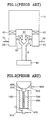
- FIG. 2 is a sectional magnified view of the air valve 60 used as a shut-off valve.
- a reference numeral 100 is a cylindrical case having orifices on the side and base thereof;
- reference numeral 200 denotes a board installed in a predetermined portion inside the case 100 to divide it into an upper part and a lower part and having a hole for communicating the lower part with the upper part in the center thereof;
- reference numeral 300 denotes a bellows fixed to the board 200 around the hole thereof to be sealed by the lower surface of the board and having an O-ring on the lower end portion thereof to open and close the base orifice of the case 100;
- reference numeral 500 denotes an elastic rubber boot installed on the internal upper surface of the case 100 and convex toward the lower part of the case 100;
- reference numeral 600 denotes a spring support fixed to the convex surface of the rubber boot 500, one portion thereof being inserted into the hole of the board 200;
- reference numeral 700 denotes a spring, one end
- the pressure of air injected through the air inlet 800 is below a predetermined value, the lower orifice of the case 100 is closed by the bellows 400. If the air pressure is greater than or equal to the predetermined pressure, the convex end portion of the rubber boot 500 is pushed upward, vertically contracting the bellows 400 and thus opening the lower orifice of the case 100. Since the lower orifice is quickly opened, the pressure of the load lock chambers 20 also rapidly drops.
- FIG. 3 shows scanning electron microspectroscopy (SEM) photographs of particles formed in the load lock chambers 20.
- the particles are about 0.3-3.7 ⁇ m in diameter and spherical in shape.
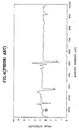
- FIG. 4 illustrates the result obtained by analyzing the components of the particles of FIG. 3 by Auger electron spectroscopy (AES).
- AES Auger electron spectroscopy
- gas condensation is found to be the cause of particle formation in an analysis of the shape and components of particles generated in the load lock chambers, as suggested by Yan Ye et al.
- the shut-off valves installed on the exhaust pipe for exhausting the load lock chambers of gas are rapidly opened, the pressure of the load lock chambers drops quickly. Therefore, particle formation is attributed to adiabatic expansion of the gas in the load lock chambers.
- European Patent Application Number 0,385,709 discloses a fluid flow control method and apparatus for minimising particle contamination.
- the fluid flow is controlled to ensure that the flow rates are maintained at values which are not high enough to dislodge particulate contaminants from the chamber walls of the apparatus.
- European Patent Application Number 0,666,339 discloses a method of in-situ cleaning a throttle valve in a chemical vapour deposition device and an exhaust flow control apparatus for facilitating such cleaning.
- the cleaning is performed using a plasma which is ignited in a cleaning gas mixture of nitrogen triflouride, hexaflouroethane and oxygen.
- the object of the present invention is to provide a semiconductor device manufacturing apparatus which can reduce condensation-induced particle formation by preventing adiabatic expansion of gas in a load lock chamber.
- a semiconductor device manufacturing apparatus comprising:
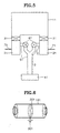
- FIG. 5 is a schematic view of a semiconductor device manufacturing apparatus, in particular an ion-implanting device, according to a first embodiment of the present invention.
- a reference numeral 11 denotes a process chamber for ion-implanting a semiconductor wafer therein;
- reference numeral 21 denotes a plurality of, for example two, load lock chambers communicating with predetermined portions of the process chamber 11 for loading semiconductor wafers to be transferred to the process chamber;
- reference numeral 31 denotes isolation valves disposed between the process chamber 11 and each load lock chamber 21 of the process chamber 11 from the load lock chambers 21;
- reference numeral 41 denotes a pump for reducing the pressure of the load lock chambers 21 to enable transfer of the wafers from the load lock chambers 21 to the process chamber 11 in vacuum;
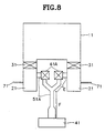
- reference numeral 51 denotes a venting pipe having a plurality (e.g., two) of sub-pipes C, each sub-pipe being connected to each load lock chamber 21, and a main pipe D
- the diameter of main pipe D is larger than that of the sub-pipes C, since gas flowing from the load lock chambers 21 is collected in and pass through the main pipe D.
- a throttle valve may be used as the venting speed controlling valve 61.
- condensation-induced particle formation can be reduced by steadily increasing a venting speed with the venting speed controlling valve 61, and thus preventing adiabatic expansion of gas caused by a rapid drop of pressure of the load lock chambers 21.
- condensation-induced particle formation can also be reduced by providing a heating source, for example, a heater line 81 in a predetermined portion of the venting gas inlet, to heat up gas injected during a venting process and thus reduce its relative humidity.
- FIG. 6 is a schematic view of a throttle valve used as the venting-speed controlling valve 61.
- a reference numeral 101 denotes a cylindrical case having orifices in the sides thereof through which the cylindrical case 101 is connected to the venting pipe 51 of FIG. 5;
- reference numeral 201 denotes a disk-shaped rotational plate for dividing case 101 into left and right parts;
- reference numeral 301 denotes a rotational shaft being rotated by a motor (not shown) and combined with the rotational plate 201 to vertically penetrate through the case 101 and pass through the center of the rotational plate 201.
- the rotational plate 201 is rotated by the rotation of the rotational shaft 301 with the rotational shaft as an axis, and the speed of gas flowing from the load lock chambers 21 to pump 41 (FIG. 5) depends on the degree of rotation.
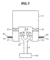
- FIG. 7 is a schematic view of a semiconductor device manufacturing apparatus, in particular an ion-implanting device, according to a second embodiment of the present invention.
- Reference numeral 61A denotes a shut-off valve installed in a predetermined portion of the sub-pipe C for shut-off of the flow of gas from the load lock chambers 21 to the pump 41.
- An air valve for example, can be used as a shut-off valve.
- a reference numeral 81 denotes a heating source installed in a predetermined portion of the venting-gas inlet 71.
- a heating line for example, can be used as the heating source.
- the heating source 81 heats up venting gas injected into the load lock chambers 21 to decrease the relative humidity of the venting gas, thereby reducing condensation-induced particle formation in the load lock chambers 21.
- condensation-induced particle formation can be reduced by preventing adiabatic expansion of gas.
Landscapes
- Chemical & Material Sciences (AREA)
- Engineering & Computer Science (AREA)
- Analytical Chemistry (AREA)
- Plasma & Fusion (AREA)
- Physics & Mathematics (AREA)
- Materials Engineering (AREA)
- Mechanical Engineering (AREA)
- Metallurgy (AREA)
- Organic Chemistry (AREA)
- Chemical Kinetics & Catalysis (AREA)
- Physical Vapour Deposition (AREA)
- Container, Conveyance, Adherence, Positioning, Of Wafer (AREA)
- Crystals, And After-Treatments Of Crystals (AREA)
Claims (5)
- Gerät zur Herstellung einer Halbleitervorrichtung umfassend:eine Prozesskammer (11) zur Fertigung einer Halbleitervorrichtung darin,eine Ladeschleusenkammer (21), die mit einem bestimmten Teil der Prozesskammer in Verbindung steht, zum Laden eines Halbleiterwafers, der in die Prozesskammer (11) zu überführen ist,eine Pumpe (41) zum Reduzieren des Druckes in der Ladeschleusenkammer (21), ein Lüftungsrohr (51), das die Ladeschleusenkammer (21) mit der Pumpe (41) verbindet, um Gas aus der Ladeschleusenkammer (21) zu entlüften, undeines oder mehrere Ventile (61), die in einem bestimmten Teil des Lüftungsrohrs installiert sind,worin das Ventil oder die Ventile (61) die Lüftungsgeschwindigkeit steuernde Ventile sind, um die Geschwindigkeit des aus der Ladeschleusenkammer (21) zur Pumpe (41) strömenden Gases zu steuern, und worin die Ladeschleusenkammer (21) einen Belüftungsgaseinlass (71) zum Einleiten von Lüftungsgas in die Ladeschleusenkammer (21) aufweist und eine in einem bestimmten Teil des Belüftungsgaseinlasses (71) installierte Wärmequelle (81).
- Gerät zur Herstellung einer Halbleitervorrichtung nach Anspruch 1, worin das die Lüftungsgeschwindigkeit steuernde Ventil oder die Ventile (61) Drosselventile sind.
- Gerät zur Herstellung einer Halbleitervorrichtung nach Anspruch 2, worin das Drosselventil oder die Drosselventile (61) umfassen:ein zylindrisches Gehäuse (101) mit in seinen beiden Seiten ausgebildeten Öffnungen zur Verbindung mit dem Lüftungsrohr (51),eine scheibenförmige Drehplatte (201) zum Unterteilen des Gehäuses (101) in einen linken und rechten Teil,eine mit der Drehplatte (201) kombinierte Rotationswelle (301), die das Gehäuse (101) vertikal durchdringt und durch die Mitte der Drehplatte (201) verläuft, undeine Kraftquelle zum Übertragen von Kraft auf die Rotationswelle.
- Gerät zur Herstellung einer Halbleitervorrichtung nach Anspruch 3, worin die Kraftquelle ein Motor ist.
- Gerät zur Herstellung einer Halbleitervorrichtung nach Anspruch 1, worin die Wärmequelle (81) eine Heizungsleitung ist, die den Lüftungsgaseinlass (71) umgibt.
Priority Applications (1)
| Application Number | Priority Date | Filing Date | Title |
|---|---|---|---|
| EP00302162A EP1017085A3 (de) | 1995-11-21 | 1996-06-07 | Gerät zur Herstellung einer Halbleitervorrichtung mit Vakuumsystem |
Applications Claiming Priority (2)
| Application Number | Priority Date | Filing Date | Title |
|---|---|---|---|
| KR1019950042623A KR100189981B1 (ko) | 1995-11-21 | 1995-11-21 | 진공 시스템을 구비한 반도체 소자 제조장치 |
| KR9542623 | 1995-11-21 |
Related Child Applications (1)
| Application Number | Title | Priority Date | Filing Date |
|---|---|---|---|
| EP00302162A Division EP1017085A3 (de) | 1995-11-21 | 1996-06-07 | Gerät zur Herstellung einer Halbleitervorrichtung mit Vakuumsystem |
Publications (2)
| Publication Number | Publication Date |
|---|---|
| EP0776026A1 EP0776026A1 (de) | 1997-05-28 |
| EP0776026B1 true EP0776026B1 (de) | 2001-10-31 |
Family
ID=19435018
Family Applications (2)
| Application Number | Title | Priority Date | Filing Date |
|---|---|---|---|
| EP96304288A Expired - Lifetime EP0776026B1 (de) | 1995-11-21 | 1996-06-07 | Gerät zur Herstellung einer Halbleitervorrichtung mit Vakuumsystem |
| EP00302162A Withdrawn EP1017085A3 (de) | 1995-11-21 | 1996-06-07 | Gerät zur Herstellung einer Halbleitervorrichtung mit Vakuumsystem |
Family Applications After (1)
| Application Number | Title | Priority Date | Filing Date |
|---|---|---|---|
| EP00302162A Withdrawn EP1017085A3 (de) | 1995-11-21 | 1996-06-07 | Gerät zur Herstellung einer Halbleitervorrichtung mit Vakuumsystem |
Country Status (7)
| Country | Link |
|---|---|
| US (2) | US5833425A (de) |
| EP (2) | EP0776026B1 (de) |
| JP (1) | JP4008515B2 (de) |
| KR (1) | KR100189981B1 (de) |
| CN (2) | CN1165637C (de) |
| DE (1) | DE69616481T2 (de) |
| TW (1) | TW308705B (de) |
Families Citing this family (33)
| Publication number | Priority date | Publication date | Assignee | Title |
|---|---|---|---|---|
| DE4117969C2 (de) * | 1991-05-31 | 2000-11-09 | Balzers Ag Liechtenstein | Vakuumkammer |
| KR100296651B1 (ko) * | 1998-07-09 | 2001-10-26 | 윤종용 | 반도체진공설비및이를이용하는방법 |
| US6161311A (en) * | 1998-07-10 | 2000-12-19 | Asm America, Inc. | System and method for reducing particles in epitaxial reactors |
| US6016611A (en) * | 1998-07-13 | 2000-01-25 | Applied Komatsu Technology, Inc. | Gas flow control in a substrate processing system |
| US6238514B1 (en) * | 1999-02-18 | 2001-05-29 | Mks Instruments, Inc. | Apparatus and method for removing condensable aluminum vapor from aluminum etch effluent |
| US6197119B1 (en) | 1999-02-18 | 2001-03-06 | Mks Instruments, Inc. | Method and apparatus for controlling polymerized teos build-up in vacuum pump lines |
| KR100740905B1 (ko) * | 2000-03-16 | 2007-07-19 | 엘지.필립스 엘시디 주식회사 | 고진공 스퍼터 장치 |
| FR2807951B1 (fr) * | 2000-04-20 | 2003-05-16 | Cit Alcatel | Procede et systeme de pompage des chambres de transfert d'equipement de semi-conducteur |
| US6568896B2 (en) | 2001-03-21 | 2003-05-27 | Applied Materials, Inc. | Transfer chamber with side wall port |
| US6488745B2 (en) | 2001-03-23 | 2002-12-03 | Mks Instruments, Inc. | Trap apparatus and method for condensable by-products of deposition reactions |
| US6701972B2 (en) | 2002-01-11 | 2004-03-09 | The Boc Group, Inc. | Vacuum load lock, system including vacuum load lock, and associated methods |
| JP2005191494A (ja) * | 2003-12-26 | 2005-07-14 | Canon Inc | 露光装置、デバイスの製造方法 |
| CN100520503C (zh) * | 2004-03-08 | 2009-07-29 | 周星工程股份有限公司 | 抽真空系统及其驱动方法、具有此系统的装置和使用此系统转移基板的方法 |
| US7253107B2 (en) * | 2004-06-17 | 2007-08-07 | Asm International N.V. | Pressure control system |
| JP4335085B2 (ja) * | 2004-07-05 | 2009-09-30 | シーケーディ株式会社 | 真空圧力制御システム |
| JP4581602B2 (ja) * | 2004-09-29 | 2010-11-17 | 株式会社島津製作所 | 真空処理装置 |
| JP2006342688A (ja) * | 2005-06-07 | 2006-12-21 | Ebara Corp | 真空排気システム |
| CN100468629C (zh) * | 2005-07-20 | 2009-03-11 | 台达电子工业股份有限公司 | 真空控制系统 |
| KR101121419B1 (ko) * | 2005-08-30 | 2012-03-15 | 주성엔지니어링(주) | 기판제조장치 및 이에 이용되는 진공펌핑방법과 벤팅방법 |
| KR100665855B1 (ko) * | 2006-02-01 | 2007-01-09 | 삼성전자주식회사 | 반도체 디바이스 제조설비의 진공장치 및 이를 이용한진공방법 |
| WO2007116676A1 (ja) * | 2006-03-31 | 2007-10-18 | Kuraray Kuraflex Co., Ltd. | 不織繊維構造を有する成形体 |
| US7989173B2 (en) * | 2006-12-27 | 2011-08-02 | The Johns Hopkins University | Detection and diagnosis of inflammatory disorders |
| KR101359401B1 (ko) * | 2007-06-21 | 2014-02-10 | 주성엔지니어링(주) | 고효율 박막 태양전지와 그 제조방법 및 제조장치 |
| JP2009252953A (ja) * | 2008-04-04 | 2009-10-29 | Hitachi High-Technologies Corp | 真空処理装置 |
| JP2010153737A (ja) * | 2008-12-26 | 2010-07-08 | Hitachi High-Technologies Corp | 真空処理装置 |
| US8623141B2 (en) * | 2009-05-18 | 2014-01-07 | Taiwan Semiconductor Manufacturing Co., Ltd. | Piping system and control for semiconductor processing |
| JP5899209B2 (ja) * | 2010-05-28 | 2016-04-06 | アクセリス テクノロジーズ, インコーポレイテッド | ワークピース上の結露を防ぐためのアクティブ露点検出およびロードロック通気 |
| EP2546300A1 (de) | 2011-07-14 | 2013-01-16 | Cytec Surface Specialties, S.A. | Strahlungshärtbare wässrige Dispersionen |
| US20140116336A1 (en) * | 2012-10-26 | 2014-05-01 | Applied Materials, Inc. | Substrate process chamber exhaust |
| KR102343637B1 (ko) * | 2019-06-13 | 2021-12-28 | 세메스 주식회사 | 기판 처리 장치 및 방법 |
| US12523380B2 (en) | 2021-08-16 | 2026-01-13 | Applied Materials, Inc. | Prevention of contamination of substrates during pressure changes in processing systems |
| US12278124B2 (en) * | 2021-10-28 | 2025-04-15 | Applied Materials, Inc. | Model-based controlled load lock pumping scheme |
| CN119650456B (zh) * | 2023-09-15 | 2025-12-12 | 北京北方华创微电子装备有限公司 | 负载锁定组件及半导体工艺设备 |
Citations (1)
| Publication number | Priority date | Publication date | Assignee | Title |
|---|---|---|---|---|
| EP0666339A1 (de) * | 1994-02-03 | 1995-08-09 | Applied Materials, Inc. | Verfahren und Anlage zur Reinigung eines Drosselventils |
Family Cites Families (20)
| Publication number | Priority date | Publication date | Assignee | Title |
|---|---|---|---|---|
| US4181288A (en) * | 1978-04-05 | 1980-01-01 | Simon Bylsma | Fluid pressure regulator valve unit for a fluid delivery system |
| US4573431A (en) * | 1983-11-16 | 1986-03-04 | Btu Engineering Corporation | Modular V-CVD diffusion furnace |
| US4657621A (en) * | 1984-10-22 | 1987-04-14 | Texas Instruments Incorporated | Low particulate vacuum chamber input/output valve |
| US4739787A (en) * | 1986-11-10 | 1988-04-26 | Stoltenberg Kevin J | Method and apparatus for improving the yield of integrated circuit devices |
| JPH01198034A (ja) * | 1988-02-03 | 1989-08-09 | Nec Yamagata Ltd | 半導体装置の製造方法 |
| JPH02185974A (ja) * | 1989-01-13 | 1990-07-20 | Tokyo Electron Ltd | 金属シリサイド膜の減圧cvd装置 |
| US4987933A (en) * | 1989-03-03 | 1991-01-29 | Eaton Corporation | Fluid flow control method and apparatus for minimizing particle contamination |
| KR0155572B1 (ko) * | 1991-05-28 | 1998-12-01 | 이노우에 아키라 | 감압처리 시스템 및 감압처리 방법 |
| JP3149206B2 (ja) * | 1991-05-30 | 2001-03-26 | 東京エレクトロン株式会社 | 熱処理装置 |
| US5228208A (en) * | 1991-06-17 | 1993-07-20 | Applied Materials, Inc. | Method of and apparatus for controlling thermal gradient in a load lock chamber |
| JPH0536618A (ja) * | 1991-08-02 | 1993-02-12 | Mitsubishi Electric Corp | 半導体製造装置 |
| JPH05218176A (ja) * | 1992-02-07 | 1993-08-27 | Tokyo Electron Tohoku Kk | 熱処理方法及び被処理体の移載方法 |
| US5303671A (en) * | 1992-02-07 | 1994-04-19 | Tokyo Electron Limited | System for continuously washing and film-forming a semiconductor wafer |
| JPH0669180A (ja) * | 1992-08-13 | 1994-03-11 | Tokyo Hightech Kk | 真空乾燥装置 |
| JP3330166B2 (ja) * | 1992-12-04 | 2002-09-30 | 東京エレクトロン株式会社 | 処理装置 |
| US5308989A (en) * | 1992-12-22 | 1994-05-03 | Eaton Corporation | Fluid flow control method and apparatus for an ion implanter |
| EP0635875B1 (de) * | 1993-02-05 | 1997-01-02 | Asm Japan K.K. | Anordnung zur thermischen behandlung. |
| JP3218488B2 (ja) * | 1993-03-16 | 2001-10-15 | 東京エレクトロン株式会社 | 処理装置 |
| US5485542A (en) * | 1994-07-18 | 1996-01-16 | Mks Instruments, Inc. | Heated fluid control valve with electric heating element and thermocouple wiring disposed in rotatable shaft |
| JPH0855810A (ja) * | 1994-08-16 | 1996-02-27 | Nec Kyushu Ltd | 拡散炉 |
-
1995
- 1995-11-21 KR KR1019950042623A patent/KR100189981B1/ko not_active Expired - Lifetime
-
1996
- 1996-05-25 TW TW085106244A patent/TW308705B/zh not_active IP Right Cessation
- 1996-06-06 CN CNB961022655A patent/CN1165637C/zh not_active Expired - Lifetime
- 1996-06-06 CN CNB200310116459XA patent/CN1242456C/zh not_active Expired - Lifetime
- 1996-06-07 EP EP96304288A patent/EP0776026B1/de not_active Expired - Lifetime
- 1996-06-07 DE DE69616481T patent/DE69616481T2/de not_active Expired - Lifetime
- 1996-06-07 EP EP00302162A patent/EP1017085A3/de not_active Withdrawn
- 1996-06-18 JP JP17750396A patent/JP4008515B2/ja not_active Expired - Lifetime
- 1996-11-20 US US08/752,954 patent/US5833425A/en not_active Expired - Lifetime
-
1997
- 1997-12-01 US US08/980,789 patent/US6071350A/en not_active Expired - Lifetime
Patent Citations (1)
| Publication number | Priority date | Publication date | Assignee | Title |
|---|---|---|---|---|
| EP0666339A1 (de) * | 1994-02-03 | 1995-08-09 | Applied Materials, Inc. | Verfahren und Anlage zur Reinigung eines Drosselventils |
Also Published As
| Publication number | Publication date |
|---|---|
| KR100189981B1 (ko) | 1999-06-01 |
| US5833425A (en) | 1998-11-10 |
| CN1501445A (zh) | 2004-06-02 |
| DE69616481T2 (de) | 2002-07-11 |
| JPH09148265A (ja) | 1997-06-06 |
| EP0776026A1 (de) | 1997-05-28 |
| EP1017085A2 (de) | 2000-07-05 |
| EP1017085A3 (de) | 2002-09-25 |
| JP4008515B2 (ja) | 2007-11-14 |
| CN1242456C (zh) | 2006-02-15 |
| TW308705B (de) | 1997-06-21 |
| DE69616481D1 (de) | 2001-12-06 |
| CN1152626A (zh) | 1997-06-25 |
| US6071350A (en) | 2000-06-06 |
| KR970030243A (ko) | 1997-06-26 |
| CN1165637C (zh) | 2004-09-08 |
Similar Documents
| Publication | Publication Date | Title |
|---|---|---|
| EP1017085A2 (de) | Gerät zur Herstellung einer Halbleitervorrichtung mit Vakuumsystem | |
| US6494959B1 (en) | Process and apparatus for cleaning a silicon surface | |
| US5073232A (en) | Method of anhydrous hydrogen fluoride etching | |
| US6042651A (en) | Molecular contamination control system | |
| US5888579A (en) | Method and apparatus for preventing particle contamination in a process chamber | |
| US20050189074A1 (en) | Gas processing apparatus and method and computer storage medium storing program for controlling same | |
| US20040129224A1 (en) | Cooling mechanism with coolant, and treatment device with cooling mechanism | |
| JPH04502981A (ja) | 半導体ウエハー処理の方法と装置 | |
| US6171104B1 (en) | Oxidation treatment method and apparatus | |
| WO2003107396A2 (en) | Substrate processing apparatus and related systems and methods | |
| US6107198A (en) | Ammonium chloride vaporizer cold trap | |
| TWI431692B (zh) | 基板處理方法及基板處理系統 | |
| KR100251876B1 (ko) | 감압 처리장치 | |
| US20230197472A1 (en) | Systems and methods for controlling moisture in semiconductor processing systems | |
| US6881952B2 (en) | Residual gas analyzer of semiconductor device manufacturing equipment | |
| JPH0729962A (ja) | 真空排気方法及び装置 | |
| KR101032043B1 (ko) | 반도체 제조설비의 가스 쿨링시스템 | |
| JPS6314866A (ja) | 超高純度ガス供給装置 | |
| KR19990042579A (ko) | 진공 시스템을 구비한 반도체 제조장치 | |
| SU1738871A1 (ru) | Устройство дл обработки изделий в вакууме | |
| Roy et al. | A novel reactor design configuration for contamination control and improved performance in the polysilicon doping process using POCl3 | |
| KR200185211Y1 (ko) | 박막 증착장치 | |
| JPH09246256A (ja) | コーティング方法ならびにそれに用いる半導体製造装置 |
Legal Events
| Date | Code | Title | Description |
|---|---|---|---|
| PUAI | Public reference made under article 153(3) epc to a published international application that has entered the european phase |
Free format text: ORIGINAL CODE: 0009012 |
|
| AK | Designated contracting states |
Kind code of ref document: A1 Designated state(s): DE FR GB IT |
|
| 17P | Request for examination filed |
Effective date: 19971001 |
|
| 17Q | First examination report despatched |
Effective date: 19990907 |
|
| GRAG | Despatch of communication of intention to grant |
Free format text: ORIGINAL CODE: EPIDOS AGRA |
|
| GRAG | Despatch of communication of intention to grant |
Free format text: ORIGINAL CODE: EPIDOS AGRA |
|
| GRAH | Despatch of communication of intention to grant a patent |
Free format text: ORIGINAL CODE: EPIDOS IGRA |
|
| GRAG | Despatch of communication of intention to grant |
Free format text: ORIGINAL CODE: EPIDOS AGRA |
|
| GRAH | Despatch of communication of intention to grant a patent |
Free format text: ORIGINAL CODE: EPIDOS IGRA |
|
| GRAH | Despatch of communication of intention to grant a patent |
Free format text: ORIGINAL CODE: EPIDOS IGRA |
|
| GRAA | (expected) grant |
Free format text: ORIGINAL CODE: 0009210 |
|
| AK | Designated contracting states |
Kind code of ref document: B1 Designated state(s): DE FR GB IT |
|
| REF | Corresponds to: |
Ref document number: 69616481 Country of ref document: DE Date of ref document: 20011206 |
|
| REG | Reference to a national code |
Ref country code: GB Ref legal event code: IF02 |
|
| ET | Fr: translation filed | ||
| PLBE | No opposition filed within time limit |
Free format text: ORIGINAL CODE: 0009261 |
|
| STAA | Information on the status of an ep patent application or granted ep patent |
Free format text: STATUS: NO OPPOSITION FILED WITHIN TIME LIMIT |
|
| 26N | No opposition filed | ||
| REG | Reference to a national code |
Ref country code: FR Ref legal event code: PLFP Year of fee payment: 20 |
|
| PGFP | Annual fee paid to national office [announced via postgrant information from national office to epo] |
Ref country code: DE Payment date: 20150521 Year of fee payment: 20 Ref country code: GB Payment date: 20150527 Year of fee payment: 20 |
|
| PGFP | Annual fee paid to national office [announced via postgrant information from national office to epo] |
Ref country code: FR Payment date: 20150526 Year of fee payment: 20 Ref country code: IT Payment date: 20150529 Year of fee payment: 20 |
|
| REG | Reference to a national code |
Ref country code: DE Ref legal event code: R071 Ref document number: 69616481 Country of ref document: DE |
|
| REG | Reference to a national code |
Ref country code: GB Ref legal event code: PE20 Expiry date: 20160606 |
|
| PG25 | Lapsed in a contracting state [announced via postgrant information from national office to epo] |
Ref country code: GB Free format text: LAPSE BECAUSE OF EXPIRATION OF PROTECTION Effective date: 20160606 |