EP0774865A2 - Caméra vidéo avec mode à grande vitesse - Google Patents
Caméra vidéo avec mode à grande vitesse Download PDFInfo
- Publication number
- EP0774865A2 EP0774865A2 EP96118290A EP96118290A EP0774865A2 EP 0774865 A2 EP0774865 A2 EP 0774865A2 EP 96118290 A EP96118290 A EP 96118290A EP 96118290 A EP96118290 A EP 96118290A EP 0774865 A2 EP0774865 A2 EP 0774865A2
- Authority
- EP
- European Patent Office
- Prior art keywords
- area
- monitor
- signal
- mode
- component value
- Prior art date
- Legal status (The legal status is an assumption and is not a legal conclusion. Google has not performed a legal analysis and makes no representation as to the accuracy of the status listed.)
- Withdrawn
Links
- 230000015654 memory Effects 0.000 claims description 97
- 238000012545 processing Methods 0.000 claims description 56
- 230000010354 integration Effects 0.000 claims description 17
- 230000006835 compression Effects 0.000 claims 1
- 238000007906 compression Methods 0.000 claims 1
- 238000001444 catalytic combustion detection Methods 0.000 description 56
- 238000012546 transfer Methods 0.000 description 33
- 238000010586 diagram Methods 0.000 description 11
- 238000000034 method Methods 0.000 description 8
- 230000008707 rearrangement Effects 0.000 description 8
- 230000001934 delay Effects 0.000 description 6
- 238000001514 detection method Methods 0.000 description 5
- 230000007274 generation of a signal involved in cell-cell signaling Effects 0.000 description 4
- 230000004044 response Effects 0.000 description 4
- 238000012937 correction Methods 0.000 description 3
- 230000003287 optical effect Effects 0.000 description 3
- 230000000630 rising effect Effects 0.000 description 3
- 238000006243 chemical reaction Methods 0.000 description 2
- 230000009977 dual effect Effects 0.000 description 2
- 238000010408 sweeping Methods 0.000 description 2
- 238000012935 Averaging Methods 0.000 description 1
- 239000003086 colorant Substances 0.000 description 1
- 230000000295 complement effect Effects 0.000 description 1
- 230000003247 decreasing effect Effects 0.000 description 1
- 230000003111 delayed effect Effects 0.000 description 1
Images


Classifications
-
- H—ELECTRICITY
- H04—ELECTRIC COMMUNICATION TECHNIQUE
- H04N—PICTORIAL COMMUNICATION, e.g. TELEVISION
- H04N25/00—Circuitry of solid-state image sensors [SSIS]; Control thereof
-
- H—ELECTRICITY
- H04—ELECTRIC COMMUNICATION TECHNIQUE
- H04N—PICTORIAL COMMUNICATION, e.g. TELEVISION
- H04N23/00—Cameras or camera modules comprising electronic image sensors; Control thereof
- H04N23/60—Control of cameras or camera modules
- H04N23/63—Control of cameras or camera modules by using electronic viewfinders
- H04N23/633—Control of cameras or camera modules by using electronic viewfinders for displaying additional information relating to control or operation of the camera
- H04N23/635—Region indicators; Field of view indicators
-
- H—ELECTRICITY
- H04—ELECTRIC COMMUNICATION TECHNIQUE
- H04N—PICTORIAL COMMUNICATION, e.g. TELEVISION
- H04N23/00—Cameras or camera modules comprising electronic image sensors; Control thereof
- H04N23/60—Control of cameras or camera modules
- H04N23/67—Focus control based on electronic image sensor signals
- H04N23/673—Focus control based on electronic image sensor signals based on contrast or high frequency components of image signals, e.g. hill climbing method
-
- H—ELECTRICITY
- H04—ELECTRIC COMMUNICATION TECHNIQUE
- H04N—PICTORIAL COMMUNICATION, e.g. TELEVISION
- H04N23/00—Cameras or camera modules comprising electronic image sensors; Control thereof
- H04N23/70—Circuitry for compensating brightness variation in the scene
- H04N23/75—Circuitry for compensating brightness variation in the scene by influencing optical camera components
-
- H—ELECTRICITY
- H04—ELECTRIC COMMUNICATION TECHNIQUE
- H04N—PICTORIAL COMMUNICATION, e.g. TELEVISION
- H04N23/00—Cameras or camera modules comprising electronic image sensors; Control thereof
- H04N23/80—Camera processing pipelines; Components thereof
- H04N23/84—Camera processing pipelines; Components thereof for processing colour signals
- H04N23/88—Camera processing pipelines; Components thereof for processing colour signals for colour balance, e.g. white-balance circuits or colour temperature control
-
- H—ELECTRICITY
- H04—ELECTRIC COMMUNICATION TECHNIQUE
- H04N—PICTORIAL COMMUNICATION, e.g. TELEVISION
- H04N23/00—Cameras or camera modules comprising electronic image sensors; Control thereof
- H04N23/80—Camera processing pipelines; Components thereof
- H04N23/84—Camera processing pipelines; Components thereof for processing colour signals
- H04N23/843—Demosaicing, e.g. interpolating colour pixel values
-
- H—ELECTRICITY
- H04—ELECTRIC COMMUNICATION TECHNIQUE
- H04N—PICTORIAL COMMUNICATION, e.g. TELEVISION
- H04N25/00—Circuitry of solid-state image sensors [SSIS]; Control thereof
- H04N25/10—Circuitry of solid-state image sensors [SSIS]; Control thereof for transforming different wavelengths into image signals
- H04N25/11—Arrangement of colour filter arrays [CFA]; Filter mosaics
- H04N25/13—Arrangement of colour filter arrays [CFA]; Filter mosaics characterised by the spectral characteristics of the filter elements
- H04N25/134—Arrangement of colour filter arrays [CFA]; Filter mosaics characterised by the spectral characteristics of the filter elements based on three different wavelength filter elements
Definitions
- the present invention relates to a video camera. More specifically, the present invention is applied to a video camera having a normal mode in which an image is displayed on a monitor by processing a camera signal outputted from all of a charge areas of a CCD imager, and a high-speed mode (a) quadruplication mode, for example in which suceeding four (4) images are displayed on the monitor by processing camera signals repeatedly outputted from one of quarter areas of the charge area, and in which picture quality associated elements such as a focus, an iris and a white balance are adjusted.
- a normal mode in which an image is displayed on a monitor by processing a camera signal outputted from all of a charge areas of a CCD imager
- a high-speed mode a quadruplication mode
- Examples of a video camera having the quadruplication mode are described in Japanese Patent Application Laying-open No. 63-250287 [H04N5/225, H04N5/30, H04N5/335, H04N3/00] laid-open on October 18, 1988, Japanese Patent Application Laying-open No. 7-212657 [H04N5/335, H01L27/12] laid-open on August 11, 1996, and a US Patent Application serial No. 08/188,543 [H04N5/335, H01L27/12] filed on January 28, 1994.
- an integration value of a high-frequency luminance signal included in a video signal to be outputted on a focus area formed at a center of a monitor is calculated, and a focus lens is moved to a position at which the integration value becomes maximum.
- the focus area FA is formed at the center of the monitor as shown in Figure 51(A), and the focus is controlled on the basis of the video signal including a main object M, and therefore, it is possible to bring the main object M in focus; however; in the quadruplication mode, the focus area FA is formed at a position deviating from the main object M as shown in Figure 51(B), and therefore, it is impossible to bring the main object M in focus.
- Such a problem also happened in controlling the iris or the white balance.
- a principal object of the present invention is to provide a video camera capable of suitably adjusting a picture quality associated element always.
- a video camera comprises: signal processing means for generating a video signal by processing a camera signal from a CCD imager; mode switching means for selectively switching a first mode and a second mode; first generating means for generating a first predetermined component value of a fist video signal based on the camera signal from a first charge area of the CCD imager at a time that the first mode is selected by the mode switching means; second generating means for generating a second predetermined component value of a second video signal based on the camera signal from a second charge area of the CCD imager at a time that the second mode is selected by the mode switching means; and adjusting means for adjusting a picture quality associated value on the basis of one of the first predetermined component value and the second predetermined component value.
- the first predetermined component value of the first video signal based on the camera signal from the first charge area of the CCD imager is generated by the first generating means, and the adjusting means adjusts the picture quality associated element on the basis of the first predetermined component value.
- the second predetermined component value of the second video signal based on the camera signal from the second charge area of the CCD imager is generated by the second generating means, and the adjusting means adjust the picture quality associated element on the basis of the second predetermined component value.
- the first generating means determines, for example, whether or not the video signal is the first video signal is to be outputted at a first monitor area of the monitor correlating to the first charge area, and generates the first predetermined component value on the basis of the determined first video signal.
- the first generating means compares first area data of the first monitor area stored in a first memory and an output position of the video signal on the monitor detected by first position detecting means, and generates the first predetermined component value at a time that the output position and the first area data are consistent with each other.
- the first mode an image corresponding to a camera signal from a whole charge area of the CCD imager is displayed on the monitor, and a single first monitor area corresponding to the first charge area is formed on the monitor.
- the second generating means determines whether or not the video signal is the second video signal to be outputted at a second monitor area of the monitor correlating to the second charge area, and generates the second predetermined component value on the basis of the determined second video signal.
- the second generating means compares second area data of the second monitor area stored in a second memory and the output position of the video signal on the monitor detected by second position detecting means, and generates the second predetermined component value at a time that the output position and the second area data are consistent with each other.
- a plurality of images corresponding to camera signals repeatedly outputted from a portion of the charge area including the second charge area are displayed on the monitor, and a single of the second monitor area corresponding to the second charge area is formed on the monitor.
- the predetermined component value utilizes for adjustment of the picture quality associated element is generated on the basis of the video signal from the monitor area corresponding to the normal mode or the quadruplication mode, it is possible to suitably adjust a picture quality always.
- a video camera comprises: signal processing means for generating a video signal by processing a camera signal from a CCD imager; mode switching means for selectively switching a first mode and a second mode; generating means for generating a predetermined component value of the video signal based on the camera signal from a predetermined charge area of the CCD imager; adjusting means for adjusting a picture quality associated element on the basis of the predetermined component value; and prohibiting means for prohibiting an operation of the adjusting means in a time that the second mode is selected by the mode switching means.
- the predetermined component value of the video signal on the basis of the camera signal from the predetermined charge area of the CCD imager is generated by the generating means, and the picture quality associated element is adjusted by the adjusting means on the basis of the predetermined component value.
- the operation of the adjusting means is prohibited by the prohibiting means. Accordingly, if the second mode is selected succeeding to the first mode, a picture quality is adjusted on the basis of the picture quality associated element adjusted in the first mode.
- the present invention in a case where the second mode is selected succeeding to the first mode, since the picture quality is adjusted according to the picture quality associated element adjusted in the first mode, it is possible to make a constitution of circuits simple.
- a video camera comprises: output control means for outputting a camera signal of a predetermined charge area of a CCD imager and sweeping-out the camera signal of a charge area excluding the predetermined charge area; generating means for generating a video signal including a plurality of video components corresponding to an output camera signal by processing the output camera signal; and zooming means for zooming the plurality of video components.
- the generating means generates the video signal including the plurality of video components corresponding to the output camera signal from the CCD imager by processing the output camera signal. Then, the plurality of video components included in the video signal are zoomed by the zooming means.
- the plurality of video components included in the video signal are zoomed, it is possible to eliminate an optical black area formed in the monitor by sweeping-out the camera signal of the charge area excluding the predetermined charge area.
- a digital video camera 10 of this embodiment shown in Figure 1 includes a CCD imager 12.
- the CCD imager 12 includes a plurality of photo-diodes 14 for photo-electric conversion, a plurality of vertical transfer CCDs 16, and horizontal transfer CCDs 20a and 20b.
- Each of the vertical transfer CCDs 16 is driven by a vertical drive circuit 18, and each of the horizontal transfer CCDs 20a and 20b is driven by a horizontal drive circuit 22.
- a drain 24 is provided in parallel to the horizontal transfer CCDs 20a and 20b. The drain 24 is utilized for sweeping-out unnecessary charges in a quadruplication mode. That is, the unnecessary charges applied from the vertical transfer CCDs 16 through sweeping-out control gates 26 are swept-out from the drain 24.
- the CCD imager 12 is provided with a mosaic type color filter with primary colors as shown in Figure 2, and a signal having 480 lines being the same as a vertical pixel number is outputted from the horizontal transfer CCDs 20a and 20b. That is, in order to increase resolution, the CCD imager 12 has dual channel structure in which all pixel data are outputted at every one field without mixing charges of pixels adjacent in a vertical direction.
- the CCD imager 12 is operated in accordance with a field storage mode as shown in Figure 4. More specifically, charges stored in the photo-diodes 14 are read-out to the vertical transfer CCDs 16 at every one field. Thereafter, a vertical transfer pulse having two succeeding rising edges at one (1) line is supplied to the vertical transfer CCDs 16, and the charges of two (2) lines are simultaneously transferred to the horizontal transfer CCDs 20a and 20b at every one line, respectively. Each of the horizontal transfer CCDs 20a and 20b outputs the charges of one line for one line period in response to a horizontal transfer clock. More specifically, the charges of odd lines such as 1, 3, 5, ...
- a charge reading pulse is supplied to the vertical transfer CCDs 16 at every quarter field as shown in Figure 6. Furthermore, each of the vertical transfer CCDs 16 is driven by a vertical transfer pulse which has two succeeding rising edges at a half line and is generated 240 times during a sweeping-out period at every quarter field. Accordingly, the charges equal to two lines are transferred to the horizontal transfer CCDs 20a and 20b at every half line.
- each of the horizontal transfer CCDs 20a and 20b is driven by a horizontal transfer clock which is the same as the horizontal transfer clock used in the normal mode, the charges of a succeeding line are started to be transferred from the vertical transfer CCDs 16 at a timing that the horizontal transfer CCDs 20a and 20b have finished transferring the first half charges and the second half charges are still remaining.
- a sweeping-out pulse is provided at that timing, and the sweeping control gate 26 is opened by the sweeping-out pulse. Accordingly, the second half charges are swept-out from the drain 24 through the sweeping control gate 26. That is, in the quadruplication mode, only the first half charges of each line are outputted from the horizontal transfer CCDs 20a and 20b, and the second half charges of each line are swept-out from the drain 24. More specifically, the first half charges of the odd lines from "1" to "239" are outputted from the horizontal transfer CCD 20a, and the first half charges of the even lines from "2" to "240" are outputted from the horizontal transfer CCD 20b.
- the charges corresponding to images shown in a left side of Figure 5(B) are outputted from the horizontal transfer CCD 20a
- the charges corresponding to images shown in a right side of Figure 5(B) are outputted from the horizontal transfer CCD 20b
- four (4) images as shown in Figure 5(C) are generated on the basis of such charges.
- the CCD imager 12 is operated in the normal mode when the quadruplication switch 28 is turned-off, and is operated in the quadruplication mode when the quadruplication switch 28 is turned-on.
- the charges, i.e. a camera signal outputted from the CCD imager 12 is applied to signal processing circuits 30a and 30b according to its channel and is subjected to processings such as automatic gain control, analog clamping, A/D conversion, digital clamping and etc. Therefore, a color camera signal is outputted from each of the signal processing circuits 30a and 30b.
- the color camera signal from the signal processing circuit 30a is applied to a contact point 132a of a switch 132 as it is, and applied to a contact point 132b of the switch 132 through a rearrangement circuit 34a.
- the color camera signal from the signal processing circuit 30b is applied to a contact point 232a of a switch 232 as it is, and applied to a contact point 232b of the switch 232 through a rearrangement circuit 34b.
- the switches 132 and 232 are interlocked with the quadruplication switch 28.
- the switches 132 and 232 are connected to the contact points 132a and 232a, respectively, when the quadruplication switch 28 is turned-off, and the switches 132 and 232 are connected to the contact points 132b and 232b, respectively, when the quadruplication switch 28 is turned-on. Accordingly, the color camera signals from the signal processing circuits 30a and 30b are outputted from the switches 132 and 232 when the quadruplication switch 28 is turned-off, and the color camera signals from the rearrangement circuits 34a and 34b are outputted from the switches 132 and 232 when the quadruplication switch 28 is turned-on.
- the rearrangement circuit 34a includes eight (8) memories a1, a2, b1, b2, c1, c2, d1 and d2, and a memory control circuit 36 as shown in Figure 7.
- Each of the memories a1, a2, b1, b2, c1, c2, d1 and d2 has a memory capacity equal to one-eighth the charge area 12', and stores a color camera signal corresponding to each of eight areas A1, A2, B1, B2, C1, C2, D1 and D2 shown in Figure 5(B). More specifically, the color camera signals corresponding to the areas A1 and A2 are alternately written into the memories a1 and a2 at every half line in a first quarter field in response to write enable signals We-a1 and We-a2.
- the color camera signals corresponding to the areas B1 and B2 are alternately written into the memories b1 and b2 at every half line in the second quarter field in response to write enable signals We-b1 and We-b2.
- the color camera signals corresponding to the areas C1, C2, D1 and D2 are succeedingly written into the memories c1, c2, d1 and d2 in response to write enable signals We-c1, We-c2, We-d1 and We-d2 in the same manner.
- read enable signals Re-a1, Re-a2, Re-b1 and Re-b2 are repeatedly applied to the memories a1, b1, a2 and b2 in this order at the first half field as shown in Figure 9. Therefore, the color camera signals are read-out from the memories a1, b1, a2 and b2.
- Read enable signals Re-c1, Re-c2, Re-d1 and Re-d2 are repeatedly applied to the memories c1, d1, c2 and d2 in this order in the second half field, and therefore, the color camera signals are read-out from the memories c1, d1, c2 and d2.
- the rearrangement circuit 34b is similar to the rearrangement circuit 34a, a duplicate description is omitted.
- the color camera signals corresponding to the images shown in Figure 5(C) are outputted from the rearrangement circuits 34a and 34b.
- the color camera signals outputted from the switches 132 and 232 are inputted to an interpolation circuit 100.
- the interpolation circuit 100 is constituted as shown in Figure 10. More specifically, the output of the first channel inputted through the switch 132 is directly applied to a selection circuit 118 as a digital signal D3, and to the selection circuit 118 as a digital signal D1 via a 1H delay 116. The output of the second channel inputted through the switch 232 is directly supplied to the selection circuit 118 as a digital signal D2, and to the selection circuit 118 via a 1H delay 117 as a digital signal D0.
- the 1H delays 116 and 117 are memories capable of storing the outputs of the first channel and the second channel for a 1H (one line) period, and the outputs of the first channel and the second channel which are delayed for the 1H period can be obtained through the 1H delays 116 and 117.
- writing operations of the 1H delays 116 and 117 and reading operations of the 1H delays 116 and 117 are executed in synchronization with operations of the horizontal transfer CCD 20a and 20b.
- the selection circuit 118 selects some digital signals equal to three lines out of the digital signals D0 to D3 of adjacent four (4) lines in accordance with whether the current field is an odd field or an even field.
- the digital signals D1 to D3 are outputted as outputs L0 to L2 at the odd field, and the digital signals D0 to D2 are outputted therefrom as outputs L0 to L2 at the even field.
- the outputs L0 to L2 of the selection circuit 118 are directly inputted to an interpolation calculation circuit 133 and a delay 130, and an output of the delay 130 is inputted to a delay 131.
- Each of the delays 130 and 131 has a delay period equal to one pixel, and outputs of the delays 130 and 131 are inputted to the interpolation calculation circuit 133. Accordingly, successive three pixels in each of the adjacent three lines, that is, signals equal to nine pixels in total are simultaneously inputted to the interpolation calculation circuit 133.
- filter elements each of which has a primary color are arranged in a mosaic fashion to form the mosaic type color filter shown in Figure 2, only one color signal out of an R signal, a G signal and a B signal is obtained from each pixel, and therefore, each of remaining color signals of each pixel is obtained by performing interpolation calculation with using around pixels by the interpolation calculation circuit 133.
- a relationship between an arrangement of the pixels on the mosaic type color filter and selected pixels is shown in Figure 11.
- the digital signal D1 to D3 are selected at the odd field, and therefore, a pixel pattern of the odd number pixels is shown in Figure 11(b), and a pixel pattern of even number pixels is shown in Figure 11(c).
- Figure 11(e) shows a portion of the arrangement of the pixels on the mosaic type color filter.
- any one of the pixel patterns shown in Figure 11(b) to Figure 11(e) is determined. Since the G signal is obtained from a center pixel in a case of Figure 11(b), for example, the G signal is outputted from the center pixel as it is. Since two R signals are obtained from two pixels at the top and the bottom of a middle vertical line, an average of the two R signals is outputted as the R signal of the center pixels. Since two B signals are obtained from two pixels of the left side and the right side of a middle horizontal line, an average of the two B signals is outputted as the B signal of the center pixel. Furthermore, in a case of Figure 11(c), each of the R signal and the G signal of the center pixel is obtained by averaging the same signals of four pixels adjacent to the center pixel.
- the R signal, the G signal and the B signal of each pixel can be obtained.
- the G signal is directly applied to a signal processing circuit 40
- each of the R signal and the B signal is applied to the signal processing circuit 40 through each of an R amplifier 38a in which a gain is controlled by an R gain control signal and a B amplifier 38b in which a gain is controlled by a B gain control signal.
- the gain of the R signal and the gain of the B signal are controlled in such manners, whereby a white balance is suitably adjusted.
- a luminance signal Y and color-difference signals R-Y and B-Y are generated by the signal processing circuit 40 on the basis of the R signal, the G signal and the B signal, whereby an image or images according to such the signals can be displayed on the monitor 55.
- the monitor 55 is not a view finder but a display unit of a television receiver, for example.
- the luminance signal Y is applied to a high-frequency luminance component value generation circuit 42 and a luminance component value generation circuit 44, and the R-Y signal is applied to an R-Y component value generation circuit 46, and the B-Y signal is applied to a B-Y component value generation circuit 48.
- each of the high-frequency luminance component value generation circuit 42, the luminance component value generation circuit 44, the R-Y component value generation circuit 46 and the B-Y component value generation circuit 48 operates as first generating means or second generating means.
- a signal determination circuit 56 as first determination means or second determination means determines whether or not the inputted luminance signal is a luminance signal to be outputted from a focus area FA or FA' formed on the monitor 55 as shown in Figure 12(A) or Figure 12(B). Furthermore, an integrating circuit 60 integrates a high-frequency component of the luminance signal obtained by passing through a high-pass filter 58. Accordingly, the high-pass filter 58 and the integrating circuit 60 operate as first predetermined component value generating means or second predetermined component value generating means.
- An integration value obtained by the integrating circuit 60 is a high-frequency luminance component value, i.e. a first predetermined component value or a second predetermined component value, and a microcomputer 50 as adjusting means controls a focus motor 52 on the basis of the high-frequency luminance component value. Therefore, a focus which is one of image quality associated elements can be adjusted.
- the luminance component value generation circuit 44 integrates, for each division area, luminance signals to be outputted from division areas D1 to D6 constituting an iris area EA and formed on the monitor 55 as shown in Figure 20(A) or division areas d1 to d6 constituting an iris area EA' and formed on the monitor 55 as shown in Figure 20(B), and each of integration values is regarded as a luminance component value, i.e. the first predetermined component value or the second predetermined component value.
- the microcomputer 50 controls an iris motor 54 on the basis of the luminance component value obtained in such a manner. That is, the microcomputer 50 as adjusting means adjusts an iris included in the image quality associated elements.
- the R-Y component value generation circuit 46 integrates, for each of division area, R-Y signals to be outputted from division areas A11 to A88 constituting an white balance area WA and formed on the monitor 55 as shown in Figure 24(A) or division areas a11 to a88 constituting an white balance area WA' and formed on the monitor 55 as shown in Figure 24(B), and each of integration values is regarded as an R-Y component value, i.e. the first predetermined component value or the second predetermined component value.
- the B-Y component value generation circuit 48 also integrates B-Y signals to be outputted from the division areas A11 to A88 or the division areas a11 to a88 in the same manner as the R-Y component value generation circuit 46, and each of integration values is regarded as a B-Y component value, i.e. the first predetermined component value or the second predetermined component value.
- the microcomputer 50 as adjusting means generates the R gain control signal and the B gain control signal on the basis of the R-Y component values and the B-Y component values, respectively so as to control each of the gains of the R amplifier 38a and the B amplifier 38b. Therefore, a white balance which is one of the image quality associated elements can be adjusted.
- the signal determination circuit 56 included in the high-frequency luminance component value generation circuit 48 is constituted as shown in Figure 14. More specifically, a vertical counter 56c, a horizontal counter 56d and a table 56e are directly connected to a CPU 56f, and area data memories 56a and 56b are connected to the CPU 56f through a switch 56h. Area data of the focus area FA shown in Figure 12(A) is stored in the area data memory 56a, and area data of the focus area FA' shown in Figure 12(B) is stored in the area data memory 56b.
- the focus area FA is constituted by sixteen (16) small areas located at a center of the monitor 55 out of sixty-four (64) small areas formed by dividing the monitor 55 into eight (8) in a vertical direction and a horizontal direction, and the focus area FA is a first monitor area. Furthermore, the focus area FA' is constituted by sixteen (16) small areas located at a center of an upper left quarter area of the monitor 56 out of sixty-four (64) small areas formed by dividing the upper left quarter area into eight (8) in the vertical direction and the horizontal direction, and the focus area FA' is a second monitor area.
- the focus area FA corresponds to a charge area FCA for focusing control and formed at a center of the charge area 12' as shown in Figure 13(A), and the focus area FA' corresponds to a charge area FCA' for focusing control and formed at a center of an upper left quarter area of the charge area 12' as shown in Figure 13(B). Then, the charge area FCA is a first charge area, and the charge area FCA' is a second charge area.
- the vertical counter 56c is incremented by a horizontal synchronization signal and reset by a vertical synchronization signal
- the horizontal counter 56d is incremented by a clock which has a rising edge for each pixel and reset by the horizontal synchronization signal.
- data of pixel positions on the monitor 55 corresponding to count values of the vertical counter 56c and the horizontal counter 56d is stored in the table 56e. That is, since there is an error between the respective count values of the vertical counter 56c and the horizontal counter 56d and the respective area data stored in the area data memories 56a and 56b, the table 56e is used for canceling such the error.
- the switch 56h is controlled by a mode signal from the quadruplication switch 28, such that the switch 56h is connected to the area data memory 56a in the normal mode, and to the area data memory 56b in the quadruplication mode.
- the CPU 56f turns-on/off a switch 56b by executing a program of a flowchart shown in Figure 15.
- each of the count values of the horizontal counter 56d and the vertical counter 56c is detected in each of steps S1 and S3, and the count values are converted into data of the pixel position from which a luminance signal which is currently being inputted is to be outputted with referring to the table 56e in a step S5.
- it is determined whether or not the pixel position is inside of the focus area FA or FA' by comparing the area data stored in the area data memory 56a or 56b of the pixel position in a Step S7. Then, if "YES”, the switch 56g is turned-on in a step S9, and if "NO", the switch 56g is turned-off in a step S11.
- the luminance signal outputted from the focus area FA is determined as a first video signal in the normal mode, and the luminance signal outputted from the focus area FA' is determined as a second video signal in the quadruplication mode.
- the area data memory 56a operates as a first memory
- the area data memory 56b operates as a second memory.
- each of the vertical counter 56c, the horizontal counter 56d, the table 56e and the CPU 56f operates as first position detecting means or second position detecting means, and the CPU 56f operates as first comparison means or second comparison means and first control means or second control means.
- the microcomputer 50 controls the focus motor 52 by executing a program indicated by flowcharts shown in Figure 16 to Figure 18.
- the high-frequency luminance component values equal to three (3) fields are detected in a Step S13, and it is determined whether or not the high-frequency luminance component values are stable in a step S15. If "NO” in the step S15, an attitude of the video camera 10 is regarded as unstable, and a processing operation returns back to the step S13; however, if "YES", the attitude of the video camera 10 is regarded as stable, a subroutine shown in Figure 18 is processed in a step S17.
- a focus lens (not shown) is moved forward for a half field period by the focus motor 52 in a step S43, and a high-frequency luminance component value 2 is detected at the lens position in a step S45.
- the focus lens is moved backward for one field period in a step S47, and a high-frequency luminance component value 1 is detected in a step S49 while the focus lens is moved.
- a high-frequency luminance component value 3 is detected in a step S51 after movement of the focus lens.
- step S19 if "NO" in the step S19, it is regarded as that the high-frequency luminance component values 2 and 3 have a relationship shown in Figure 19(B) or Figure 19(C), and the high-frequency luminance component values 2 and 3 are compared with each other in a step S21. Then, if the relationship shown in Figure 19(B), a moving direction of the focus lens is inverted in a step S23; however, if the relationship shown in Figure 19(C), the processing operation proceeds to a step S25 without inverting the moving direction of the focus lens. Accordingly, the focus lens is moved in a determined direction in the step S25, and thereafter, the high-frequency luminance component value is detected in a step S27.
- step S35 the same processing as that of the step S19 is executed in a step S35, and if "NO”, the processing operation returns back to the step S21; however, if "YES”, the processing operation proceeds to the step S37.
- the microcomputer 50 since the high-frequency luminance component value is generated from the focus area FA or FA' in accordance with the normal mode or the quadruplication mode, the microcomputer 50 suitably focuses the focus lens on the main object M shown in Figure 12(A) and (B) without executing difference processing for each mode.
- the luminance component value generation circuit 44 is constituted as shown in Figure 21. More specifically, area data memories 44a and 44b are connected to a CPU 44f via a switch 44j controlled by the mode signal from the quadruplication switch 28, and a vertical counter 44c, a horizontal counter 44d and a table 44e are directly connected to the CPU 44f. Area data of the respective division areas D1 to D6 formed on the monitor 55 as shown in Figure 20(A) are stored in the area data memory 44a, and area data of the respective division areas d1 to d6 formed on the upper left quarter area of the monitor 55 as shown in Figure 20(B) are stored in the area data memory 44b. In addition, the iris area EA constituted by the division areas D1 to D6 is the first monitor area, and the iris area EA' constituted by the division areas d1 to d6 is the second monitor area.
- the iris area EA corresponds to the charge area ECA having the same scale as the charge area 12' shown in Figure 13(A), and the iris area EA' corresponds to the charge area ECA' formed on the upper left quarter area of the charge area 12' as shown in Figure 13(B). Then, the charge area ECA is the first charge area, and the charge area ECA' is the second charge area.
- the vertical counter 44c and the horizontal counter 44d are operated in the same manner as the vertical counter 56c and the horizontal counter 56d of the signal determination circuit 56, and the table 44e has the same data as that of the table 56e. Accordingly, by converting the count values into data stored in the table 44e, it is possible to correct an error between the count values of the vertical counter 56c and the horizontal counter 56d and the pixel position from which a luminance signal is to be outputted.
- the switch 44h is controlled by the CPU 44f, whereby a reading signal and a writing signal outputted from a signal generation circuit 44g are applied to any of registers m1 to m6. Accordingly, data read-out from any of the registers m1 to m6 is added to the luminance signal by an adder 44i, and added data is written into the same register. Since the registers m1 to m6 are initialized by the vertical synchronization signal, integration values of luminance signals outputted from the division areas D1 to D6 or the division areas d1 to d6 are obtained by the registers m1 to m6, respectively.
- the CPU 44f controls the switch 44h by executing a program of a flowchart shown in Figure 22.
- each of the count values of the horizontal counter 44d and the vertical counter 44c is detected in each of steps S53 and S55, and the count values are converted into the pixel position with using the table 44e in a step S57.
- one of the division areas D1 to D6 in which the pixel position exists is determined in steps S5901 to S5906 in the normal mode, and one of the division areas d1 to d6 in which the pixel position exists is determined in the steps S5901 to S5906 in the quadruplication mode.
- the switch 44h is connected to any of the registers m1 to m6 in accordance with a determination result at steps S6101 to S6106. Therefore, a plurality of luminance component values corresponding to the division areas D1 to D6 are obtained as a plurality of the first predetermined component values in the normal mode, and a plurality of luminance component values corresponding to the division areas d1 to d6 are obtained as a plurality of the second predetermined component values.
- the area data memories 44a and 44b, the vertical counter 44c, the horizontal counter 44d, the table 44e and the CPU 44f are operated as the first determination means or the second determination means.
- the vertical counter 44c, the horizontal counter 44d, the table 44e and the CPU 44f is operated as the first position detecting means or the second position detecting means, and the CPU 44f is operated as the first comparison means or the second comparison means, and the first control means or the second control means.
- the adder 44i, the switch 44h, the signal generation circuit 44g and the registers m1 to m6 are operated as the first predetermined component value generating means or the second predetermined component value generating means.
- the microcomputer 50 receives the luminance component values and executes a flowchart shown in Figure 23. According to the flowchart, a count value k of a counter 50a is set into "1" in a step S63, and each of weights W1 to W6 is set into an initial value in a step S65. In addition, the weights W1 to W3 have the same value, and the weights W4 to W6 also have the same value, and the weights W1 to W3 are larger than the weights W4 to W6.
- luminance component values Y1 to Y6 corresponding to the division areas D1 to D6 or d1 to d6 are detected in a step S67, and it is determined whether or not the luminance component value Yk (k is the count value) is much larger than a reference value in a step S69. Then, if "YES”, the weight Wk is set into “0" in a step S71, and a processing operation returns back to the step S69; however, if "NO”, it is determined whether or not the count value k is equal to "6" in a step S73. Then, if "NO", the counter 50a is incremented in a step S75, and the processing operation returns back to the step S69.
- an average value YW AV of weighted luminance component values is calculated in a step S77, and a relationship between the average value YW AV and the reference value is determined in steps S79 and S81. If the average value YW AV is larger than the reference value, the iris motor 54 is driven such that the iris is closed in a step S83. If the average value YW AV is smaller than the reference value, the iris motor 54 is driven such that the iris is opened in a step S85. If the average value YW AV is equal to the reference value, the iris motor 54 is stopped in a step S87.
- the microcomputer 50 suitably controls the iris without changing the processing operation in accordance with the mode.
- the R-Y component value generation circuit 46 is constituted as shown in Figure 25; however, since the R-Y component value generation circuit 46 is the same or similar to the luminance component value generation circuit 44 unless sixty-four (64) registers n1 to n64 are provided instead of the registers m1 to m8, a duplicate description will be omitted.
- Area data of small areas obtained by dividing the monitor 55 into eight (8) in the vertical direction and the horizontal direction as shown in Figure 24(A) is stored in the area data memory 46a
- area data of small areas obtained by dividing the upper left quarter area of the monitor 55 into eight (8) in the vertical direction and the horizontal direction as shown in Figure 24(B) is stored in the area data memory 46b.
- the small areas shown in Figure 24(A) are the division areas A11 to A88, respectively
- the small areas shown in Figure 24(B) are the division areas a11 to a88, respectively.
- the white balance area WA is constituted by the division areas A11 to A88
- the white balance area WA' is constituted by the division areas a11 to a88.
- the white balance area WA is the first monitor area
- the white balance area WA' is the second monitor area.
- a two-digit numbers attached to "A" and "a” show positions of the small areas. That is, upper digit numbers show positions in the vertical direction, and lower digit numbers show positions in the horizontal direction.
- the white balance area WA corresponds to the charge area WCA having the same scale as the charge area 12' shown in Figure 13(A), and the white balance area WA' corresponds to the charge area WCA' formed on the upper left quarter area of the charge area 12' as shown in Figure 13(B). Then, the charge area WCA is the first charge area, and the charge area WCA' is the second charge area.
- a switch 46j is connected to an area data memory 46a in the normal mode, and connected to an area data memory 46b in the quadruplication mode.
- a CPU 46f controls a switch 46h by processing a flowchart shown in Figure 26. According to the flowchart, each of count values of a horizontal counter 46b and a vertical counter 46c is detected in each of steps S89 and S91, and the count values are converted into a pixel position from which an R-Y signal is to be outputted with using a table 46e.
- one of the division areas A11 to A88 in which the pixel position exists is determined in steps S9501 to S9564 in the normal mode, and one of the division areas a11 to a88 in which the pixel position exists is determined in the steps S9501 to S9564 in the quadruplication mode.
- the switch 46h is connected to any of the registers n1 to n64 in any of steps S9701 to S9764.
- a reading signal and a writing signal from the signal generation circuit 46g are applied to a desired register, and integration values of the division areas A11 to A88, i.e. the R-Y component values are obtained by the registers n1 to n64, respectively, in the normal mode, and integration values of the division areas a11 to a88, that is, the R-Y component values are obtained by the registers n1 to n64, respectively, in the quadruplication mode.
- Each of the R-Y component values is the first predetermined component value or the second predetermined component value. Accordingly, an adder 46i, the switch 46h, the signal generation circuit 46g and the registers n1 to n64 are operated as the first predetermined component value generating means or the second predetermined component value generating means.
- B-Y component value generation circuit 48 has the same structure as that of the R-Y component value generation circuit 46, a duplicate description is omitted here by adding reference numerals in parentheses in Figure 25.
- the microcomputer 50 receives the R-Y component values and the B-Y component values generated by the R-Y component value generation circuit 46 and the B-Y component value generation circuit 48, respectively, and generates the R gain control signal and the B gain control signal by processing flowcharts shown in Figure 27 to Figure 29.
- the R-Y component values and the B-Y component values are detected in a step S101, and weights W 1,1 to W 8,8 are adjusted by processing a subroutine shown in Figure 28 and Figure 29. Thereafter, average values (R-Y) AV and (B-Y) AV are calculated with using the weights W 1,1 to W 8,8 in a step S105, and gain correction amounts of the R amplifier 38a and the B amplifier 38b are determined in a step S107. Then, the R gain control signal according to one of the gain correction amounts and the B gain control signal according to other one of the gain correction amounts are outputted in a step S109.
- variables C1 and C2 are set into a first threshold value and a second threshold value, respectively, in a step S111, and each of variables x and y is set into "8" in a step S113.
- the variables x and y show numbers of the division areas A11 to A88 or a11 to a88 in the vertical direction and the horizontal direction, respectively.
- each of a count value j of a counter 50b and a count value i of a counter 50c is set into "1" in each of steps S115 and S117, and the weight W i,j is set into "1" in a step S119.
- step S121 it is determined whether or not the count value i is equal to "1" in a step S121. If “YES”, since a noted or target division area is a top, and it is impossible to compare with an upper division area of the noted division area, a processing operation directly proceeds to a step S129. However, if "NO" in the step S121, it is determined whether or not formulas (1) and (2) are satisfied in steps S123 and S125, respectively. If even one of the formulas (1) and (2) is not satisfied, the processing operation directly proceeds to the step S129; however, if both of the formulas (1) and (2) are satisfied, the weight W i,j is halved in a step S127, and the processing operation proceeds to the S129.
- step S129 It is determined whether or not the count value j is equal to "1" in the step S129. If “YES”, since the noted or target division area exists at a left end, and it is impossible to compare with a left-adjacent division area to the noted division area, the processing operation directly proceeds to a step S137. However, if the count value j is not equal to "1", it is determined whether or not each of formulas (3) and (4) is satisfied in each of steps S131 and S133. If even one of the formulas (3) and (4) is not satisfied, the processing operation proceeds to the step S137; however, if both of the formulas (3) and (4) are satisfied, the weight W i,j is halved in a step S135.
- the weight W i,j is halved. Accordingly, if all of the formulas (1) to (4) are satisfied, the weight W i,j is quartered. (3)
- the count value i is incremented in the step S137, and it is determined whether or not the count value i is larger than the variable y in a step S139. Then, if "NO”, processes of the step S119 and afterward are repeated; however, if "YES”, the count value j is incremented in a step S141, and the processing operation proceeds to a step S143. It is determined whether or not the count value j is larger than the variable x in the step S143, and if "NO”, processes of the step S117 and afterward are repeatedly executed, and if "YES", the processing operation is finished.
- the weight w i,j is adjusted for each division area, and the average values (R-Y) AV and (B-Y) AV are calculated in the step S105.
- the microcomputer 50 since the R-Y component value generation circuit 46 and the B-Y component value generation circuit 48 generate the R-Y component value and the B-Y component value in accordance with the normal mode or quadruplication mode, the microcomputer 50 suitably generates the R gain control signal and the B gain control signal by processing the same program, and therefore, it is possible to suitably adjust the white balance irrespective of the mode.
- the camera signal is actually processed as shown in Figure 30(A) to Figure 30(C) in the quadruplication mode. More specifically, though Figure 5(C) is drawn such as the four (4) images to be displayed are touched with each other, it is necessary to secure a period for sweeping-out the charges of the second half of each line in the horizontal direction and the charges of the second half of each quarter field in the vertical direction. In such the period, since the horizontal transfer CCDs 20a and 20b operates to output the charges even though input gates of the horizontal transfer CCDs 20a and 20b are closed, an output-indefinite area in which an output becomes indefinite or uncertain is actually formed at a diagonal line area shown in Figure 30(C).
- each of the four (4) images displayed on the monitor 55 has 297 pixels and 164 lines, and the output-indefinite area has 63 pixels at its right side and 16 lines at its lower side.
- area data of a focus area FA' shown in Figure 31 is written into the area data memory 56b included in the signal determination circuit 56. More specifically, sixteen (16) small areas at a center of an area having 297 pixels and 164 lines and formed on an upper left side of the monitor 55 out of sixty-four (64) small areas obtained by dividing the area into eight (8) in the horizontal direction and the vertical direction constitute the focus area FA', and the area data of the focus area FA' is written into the area data memory 56b.
- area data of the division areas d1 to d6 included in an iris area EA' shown in Figure 32 is stored in the area data memory 44b of the luminance component value generation circuit 44.
- the division areas d1 to d6 are also constituted by the small areas described above with using Figure 31.
- area data of the division areas a11 to a88 included in a white balance area WA' shown in Figure 33 is stored in the area data memory 46b of the R-Y component value generation circuit 46 and the area data memory 48b of the B-Y component value generation circuit 48.
- each of the small areas described above with using the Figure 31 is each of the division areas a11 to a88, and the respective area data are stored in the area data memory 46b and 48b.
- a high-frequency luminance component value, R-Y component values and B-Y component values generated are unaffected by the output-indefinite area, and therefore, it is possible to suitably control the focus, the iris and the white balance in the quadruplication mode.
- the area data memories 46a and 48a for the normal mode in the quadruplication mode since the microcomputer 50 executes a processing operation except the R-Y component values and the B-Y component values of division areas overlapping on the output-indefinite area, the area data memories 46b and 48b for the quadruplication mode becomes unnecessary, and it is possible to make the structure simple.
- the microcomputer 50 detects the high-frequency luminance component value 1 while the focus lens is moved in the step S49 shown in Figure 18, the focus area FA' is formed on the upper left quarter area of the monitor 55 as shown in Figure 13(B) in the quadruplication mode. Accordingly, the high-frequency luminance component value 1 is obtained at a position close to 2 not a position of 1 shown in Figure 19 in the quadruplication mode, and therefore, there is a possibility that accuracy of the focusing control is decreased in comparison with the normal mode.
- focus areas FA' are formed for all the four images displayed on the monitor 55 as shown in Figure 36, and area data of the focus areas FA' are stored in the area data memory 56b. That is, the second monitor areas of the same number as that of the displayed images are formed on the monitor 55.
- the area data of the division areas A11 to A88 obtained by dividing the monitor 55 as shown in Figure 24(A) is stored in the area data memories 46a and 48a shown in Figure 24 in the normal mode, in taking the object at a wide-angle, for example, there is a possibility that the white balance can not be suitably controlled due to small number of division areas.
- the R-Y component value generation circuit 46 is constituted as shown in Figure 37. More specifically, area data memories 46b, 46m, 46n and 46p are further provided, and the area data memories 46m, 46n and 46p are connected to the CPU 46f through a switch 46k and the switch 46j. Furthermore, the switch 46j is connected to the switch 46k in the quadruplication mode and a wide-angle mode (both of them are the second mode), and the switch 46k is changed at every one field by the CPU 46f in such the modes.
- area data of division areas ⁇ 11 to ⁇ 88 formed at an upper right quarter area on the monitor 55 as shown in Figure 40(B) is stored in the area data memory 46m
- area data of division areas ⁇ 11 to ⁇ 88 formed at a lower left quarter area on the monitor 55 as shown in Figure 40(C) is stored in the area data memory 46n
- area data of division areas ⁇ 11 to ⁇ 88 formed at a lower right quarter area on the monitor 55 as shown in Figure 40(D) is stored in the area data memory 46p.
- the CPU 46f processes flowcharts shown in Figure 41 and Figure 42 in the quadruplication mode and the wide-angle mode in order to generate the R-Y component value for each division area in a four (4) field period.
- an area counter 46r is initialized in a step S145, and it is determined whether or not the vertical synchronization signal is inputted in a step S147. Then, if "NO”, a processing operation directly proceeds to a step S151; however, if "YES", the switch 46k is changed in accordance with a count value of the area counter 46i in a step S149, and then, the processing operation proceeds to the step S151.
- a count value of the horizontal counter 46d is detected in the step S151, and a count value of the vertical counter 46c is detected in a step S153, and the count values of the horizontal counter 46d and the vertical counter 46c are converted into data of a pixel position from which an R-Y signal is to be outputted with using the table 46e in a step S155.
- one of the division areas in which the pixel position exists is determined in steps S15701 to S15764. More specifically, one of the division areas A11 to A88 in which the pixel position exists, one of the division areas ⁇ 11 to ⁇ 88 in which the pixel position exists, and one of the division areas ⁇ 11 to ⁇ 88 in which the pixel position exists, or one of the division areas ⁇ 11 to ⁇ 88 in which the pixel position exists is determined in the steps S15701 to S15764. Then, the switch 46h is connected to a desired register in accordance with a determination result in any one of steps S15901 to S15964.
- the division areas used for the processing operation are changed at every one field. Therefore, it is possible to form division areas of four-times the number of the division areas on the monitor 55 in the normal mode as shown in Figure 39, and it is possible to generate four-times the number of R-Y component values. Accordingly, it is possible to perform the white balance control with high-accuracy and without increasing the number of the registers in the wide-angle mode.
- the B-Y component value generation circuit 48 of this embodiment is also constituted in the same manner as the R-Y component value generation circuit 46, a duplicate description is omitted by adding numeral numbers in parenthes in Figure 37.
- a high-frequency luminance component value generation circuit 42', a luminance component value generation circuit 44', and an R-Y component value generation circuit 46' and a B-Y component value generation circuit 48' perform the same operations irrespective of the normal mode or the quadruplication mode.
- the high-frequency luminance component value generation circuit 42' generates only the high-frequency luminance component value of the focus area FA shown in Figure 12(A)
- the luminance component value generation circuit 44' generates only the luminance component values of the division areas D1 to D6 shown in Figure 20(A)
- the R-Y component value generation circuit 46' and the B-Y component value generation circuit 48' generate only the R-Y component values and the R-Y component values of the division areas A11 to A88 shown in Figure 24(A).
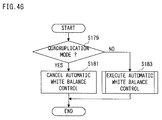
- the microcomputer 50' processes a flowchart shown in Figure 44 in the focusing control, processes a flowchart shown in Figure 45 in the iris control, and processes a flowchart shown in Figure 46 in the white balance control.
- a mode is the quadruplication mode in a step S167, and if "NO”, an automatic focusing control is executed in a step S171; however, if "YES”, the automatic focusing control is canceled.
- the iris control it is determined whether or not a mode is the quadruplication mode in a step S173, and if "NO”, an automatic iris control is executed in a step S177; however, if "YES", the automatic iris control is canceled in a step S175.
- a mode is the quadruplication mode in a step S179, and if "NO”, the automatic white balance control is executed in a step S183; however, if "YES”, the automatic white balance control is canceled in a step S181.
- a zooming-up circuit 62 is connected to the signal processing circuit 40 through a switch (not shown) which is turned-on in the quadruplication mode. Accordingly, in the quadruplication mode, the video signals equal to one field, i.e. the luminance signal Y the R-Y signal and the B-Y signal equal to one field outputted from the signal processing circuit 40 are written into field memories 64a to 64c, respectively, in accordance with a writing control signal from a writing control circuit 66.
- Written video signals are read-out therefrom by a reading control signal from a reading control circuit 68. That is, the reading control circuit 68 receives a line designation signal from a coefficient generation circuit 70, and reads-out the video signals from a designated line and a succeeding line of the field memories 64a to 64c.
- the a luminance signal read-out from the designated line of the field memory 64a is applied to a multiplier 72a, and the luminance signal read-out from the succeeding line of the memory 64a is applied to a multiplier 72b.
- the R-Y signal read-out from the designated line of the field memory 64b is applied to a multiplier 72c, and the R-Y signal read-out from the succeeding line of the memory 64b is applied to a multiplier 72d.
- the B-Y signal read-out from the designated line of the field memory 64c is applied to a multiplier 72e, and the B-Y signal read-out from the succeeding line of the memory 64b is applied to a multiplier 72f.
- Each of the luminance signal Y, the R-Y signal and the B-Y signal applied to each of the multipliers 72b, 72d and 72f is multiplied by a coefficient "K" outputted from the coefficient generation circuit 70, and multiplication results are applied to adders 74a to 74c, respectively. Furthermore, each of the luminance signal Y, the R-Y signal and the B-Y signal applied to each of the multiplier 72a, 72c and 72f is multiplied by a coefficient "1-K" outputted from the coefficient generation circuit 70, and multiplication results are applied to the adder 74a to 74c, respectively.
- a luminance signal Y, an R-Y signal and a B-Y signal each of which is zoomed-up in the vertical direction are obtained as first zoom-up components.
- the luminance signal Y, the R-Y signal and the B-Y signal zoomed-up are written into line memories 77a to 77c by a writing control signal from a writing control circuit 78 at every one line, respectively, and read-out therefrom by a reading control signal from a reading control circuit 80 until writing of a succeeding line are started. That is, the reading control circuit 80 receives a pixel designation signal from a coefficient generation circuit 82, and reads-out the video signals from a designated pixel position and a succeeding pixel position.
- the luminance signal read-out from the designated pixel position of the line memory 77a is applied to a multiplier 84a, and the luminance signal read-out from the succeeding pixel position of the memory 77a is applied to a multiplier 84b. Furthermore, the R-Y signal read-out from the designated pixel position of the line memory 77b is applied to a multiplier 84c, and the R-Y signal read-out from the succeeding pixel position of the memory 77b is applied to a multiplier 84d.
- the B-Y signal read-out from the designated pixel position of the line memory 77c is applied to a multiplier 84e, and the B-Y signal read-out from the succeeding pixel position of the memory 77c is applied to a multiplier 84f.
- Each of the luminance signal Y, the R-Y signal and the B-Y signal applied to each of the multiplier 84b, 84d and 84f is multiplied by a coefficient "L" outputted from the coefficient generation circuit 82, and multiplication results are applied to adders 86a to 86c, respectively. Furthermore, each of the luminance signal Y, the R-Y signal and the B-Y signal applied to each of the multipliers 84a, 84c and 84e is multiplied by a coefficient "1-L" outputted from the coefficient generation circuit 82, and multiplication results are applied to the adders 86a to 86c, respectively. Accordingly, a luminance signal Y, an R-Y signal and a B-Y signal each of which is zoomed-up in the vertical direction and the horizontal direction are outputted from the adders 86a to 86c, respectively.
- a three-port memory "CSK-48323" manufactured by SONY can be used for the field memories 64a to 64c and the line memories 77a to 77c.
- the coefficient generation circuit 70 is constituted as shown in Figure 48.
- a reciprocal number "1/Z" of a zoom-up ratio "Z” is stored in a register 70a, and an initial value is stored in a register 70b.
- the zoom-up ratio "Z” is "1.21", and the reciprocal number is "0.8”.
- a vertical counter 70k is reset by the vertical synchronization signal from the timing generator 76, and incremented by the horizontal synchronization signal, and a count value of the vertical counter 70k is applied to a comparator 70d.
- the comparator 70d compares the count value with reference values "0" and "180", and connects a switch 70c to the register 70b at a time that the count value is consistent with one of the reference values. In contrast, if the count value is not consistent with the reference values, the comparator 70d connects the switch 70c to the register 70a.
- the initial value outputted from the register 70b is applied to an adder 70e in reading-out the video signals from respective first lines of four (4) image areas which are formed in respective ones of the field memories 64a to 64c as shown in Figure 50, and the reciprocal number outputted from the register 70a is applied to the adder 70e in reading-out other video signals.
- the adder 70e integrates an inputted value at every one line. Then, the adder 70e applies an integration value to a detection circuit 70f, and applies a value before the decimal point of the integration value to an adder 70h. In addition, the adder 70e is initialized at every time that the switch 70c is changed to the register 70b.
- the detection circuit 70f detects a value after the decimal point of the integration value so as to output the value as the coefficient "K” and to apply the value, i.e. "K” to a subtraction circuit 70g.
- the subtraction circuit 70g subtracts the coefficient "K” from “1”, and outputs a subtraction result as the coefficient "1-K”.
- the count value of the vertical counter 70k is also applied to an area determination circuit 70j.
- the area determination circuit 70j outputs an area determination signal of a high level at a time that the count value is any of "0" to "179", and outputs an area determination signal of a low level at a time that the count value is any of "180" to "359".
- the area determination circuit 70j outputs the area determination signal as shown in Figure 50.
- a reference value generator 70i outputs a reference value "0" at a time that the area determination signal is the high level, and outputs a reference value "180" at a time that the area determination signal is the low level.
- the adder 70h adds a value from the adder 70e and a reference value from the reference value generator 70i each other, and outputs an addition result as the line destination signal.
- the line designation signal has the same value, and therefore, the same signal is succeedingly read-out from respective one of the field memories 64a to 64c. Furthermore, since the value after the decimal point of the integration value is detected by the detection circuit 70f, the coefficient "K" has a value between "0" to "1". Accordingly, the signals read-out from predetermined two lines of the field memory 64a are weighted by predetermined ratios by the multiplier 72a and 72b, and weighted signals are added to each other by the adder 74a.
- the signals read-out from predetermined two lines of the field memory 64b are weighted by the predetermined ratios by the multipliers 72c and 72d, and weighted signals are added to each other by the adder 74b.
- the signals read-out from predetermined two lines of the field memory 64c are weighted by the predetermined ratios by the multipliers 72e and 72f, and weighted signals are added to each other by the adder 74c.
- the switch 70c In generating a video signal to be outputted at a first line on the monitor 55, for example, the switch 70c is connected to the register 70b, whereby the initial value "0" is applied to the adder 70e.
- the reference value "0" is applied to the adder 70h from the reference value generator 70i. Accordingly, the coefficient "K” indicates “0", and the coefficient "1-K” indicates “1”, and the line designation signal indicates "0".
- a weight for signals applied to the multipliers 72a, 72c and 72e becomes “1"
- a weight for signals applied to the multipliers 72b, 72d and 72f becomes "0”
- the signals read-out from first lines of the field memories 64a to 64c are outputted as they are from the adders 74a to 74c, respectively.
- signals being read-out from the field memory 64a and weighted are added to each other by the adder 74a
- signals being read-out from the field memory 64b and weighted are added to each other by the adder 74b
- signals being read-out from the field memory 64c and weighted are added to each other by the adder 74c.
- video signals stored in an upper half image areas of respective one of the field memories 64a to 64c are zoomed-up in the vertical direction.
- no video signals are read-out from the output-indefinite area formed in the respective one of the field memories 64a to 64c because if a video signal to be outputted at 179th line of the monitor 55 is generated, the switch 70c is connected to the register 70b, and therefore, the reference value "180" is outputted from the reference value generator 70i, and reading-out of video signals is started from 180th line of the field memories 64a to 64c.
- a zooming-up operation of video signals stored in a lower half image areas of respective one of the field memories 64a to 64c in a vertical direction is succeedingly executed.
- a horizontal counter 82k is incremented by the clock from the timing generator 76, and reset by the horizontal synchronization signal.
- a comparator 82d changes a switch 82c to a register 82b at only a time that a count value of the horizontal counter 82k is "0" or "360".
- a detection circuit 82f detects a value after the decimal point of an integration value obtained by an adder 82e at every one pixel, and outputs the value as the coefficient "L”.
- a subtraction circuit 82g subtracts the coefficient "L” from “1", and outputs a subtraction value as the coefficient "1-L".
- An area determination circuit 82j outputs an area determination signal shown in Figure 50 in accordance with the count value of the horizontal counter 82k. More specifically, the area determination signal is a high level at a time that the count value is any one from “0” to “359", and the area determination signal is a low level at a time that the count value is any one from “360” to "719". Then, a reference value generator 82i outputs a reference value "0" at a time that the area determination signal is the high level, and outputs a reference value "360” at a time that the area determination signal is the low level.
- each of video signals written into the line memories 77a to 77c is zoomed-up in the horizontal direction.
- the coefficient "L” is “0", and the coefficient "1-L” is “1". Furthermore, the pixel destination signal indicates "0". Accordingly, video signals stored in first pixel positions of the line memories 77a to 77c are outputted as they are from the adders 86a to 86c, respectively.
- the coefficient "L” is "0.8", and the coefficient "1-L” is “0.2”, and the pixel destination signal indicates "0".
- each of the video signals read-out from the first pixel positions of the line memories 77a to 77c is multiplied by "0.2", and each of video signals read-out from second pixel positions thereof are multiplied by "0.8". Then, video signals being read-out from the line memory 77a and weighted are added to each other by the adder 86a, and video signals being read-out from the line memory 77b and weighted are added to each other by the adder 86b, and video signals being read-out from the line memory 77c and weighted are added to each other by the adder 86c.
- each of the video signals stored in the line memories 77a to 77c is zoomed-up in the horizontal direction.
- no video signals are read-out from the output-indefinite areas formed on the line memories 77a to 77c.
- the four (4) images to be displayed on the monitor 55 are zoomed-up in the horizontal direction and the vertical direction by the zooming-up circuit 62, it is possible to delete the output-indefinite area from the monitor 55.
- a color filter of a complementary color can be used instead of a color filter of a primary color.
- each of the high-frequency luminance component value generation circuit, the luminance component value generation circuit, the R-Y component value generation circuit and the B-Y component value generation circuit is provided with the area data memories; however, if the respective circuits share a single area data memory for each mode while the microcomputer 50 processes necessary one of the high-frequency luminance component value, the luminance component values, the R-Y component values and the B-Y component values, it is possible to reduce the number of the memories.
- the present invention can be applied to a case that the CCD imager is moved in an optical axis direction.
Landscapes
- Engineering & Computer Science (AREA)
- Multimedia (AREA)
- Signal Processing (AREA)
- Studio Devices (AREA)
- Automatic Focus Adjustment (AREA)
Applications Claiming Priority (6)
| Application Number | Priority Date | Filing Date | Title |
|---|---|---|---|
| JP30022695 | 1995-11-17 | ||
| JP300225/95 | 1995-11-17 | ||
| JP30022695 | 1995-11-17 | ||
| JP30022595A JP3389385B2 (ja) | 1995-11-17 | 1995-11-17 | ビデオカメラ |
| JP30022595 | 1995-11-17 | ||
| JP300226/95 | 1995-11-17 |
Publications (2)
| Publication Number | Publication Date |
|---|---|
| EP0774865A2 true EP0774865A2 (fr) | 1997-05-21 |
| EP0774865A3 EP0774865A3 (fr) | 2000-06-07 |
Family
ID=26562265
Family Applications (1)
| Application Number | Title | Priority Date | Filing Date |
|---|---|---|---|
| EP96118290A Withdrawn EP0774865A3 (fr) | 1995-11-17 | 1996-11-14 | Caméra vidéo avec mode à grande vitesse |
Country Status (2)
| Country | Link |
|---|---|
| US (1) | US6005612A (fr) |
| EP (1) | EP0774865A3 (fr) |
Cited By (17)
| Publication number | Priority date | Publication date | Assignee | Title |
|---|---|---|---|---|
| WO1999053832A1 (fr) * | 1998-04-20 | 1999-10-28 | Xillix Technologies Corp. | Systeme d'imagerie avec commande de gain automatique pour endoscopie par reflectance et fluorescence |
| EP0975153A1 (fr) * | 1998-07-24 | 2000-01-26 | Matsushita Electric Industrial Co., Ltd. | Appareil de prise de vues |
| WO2003105485A1 (fr) * | 2002-06-06 | 2003-12-18 | Leica Microsystems (Schweiz) Ag | Procede et systeme pour analyser un enregistrement optique |
| EP1437886A1 (fr) * | 2001-10-03 | 2004-07-14 | Sony Corporation | Imageur et procede de correction de qualite |
| US6821245B2 (en) | 2000-07-14 | 2004-11-23 | Xillix Technologies Corporation | Compact fluorescence endoscopy video system |
| US9386909B2 (en) | 2006-07-28 | 2016-07-12 | Novadaq Technologies Inc. | System and method for deposition and removal of an optical element on an endoscope objective |
| US9642532B2 (en) | 2008-03-18 | 2017-05-09 | Novadaq Technologies Inc. | Imaging system for combined full-color reflectance and near-infrared imaging |
| US9814378B2 (en) | 2011-03-08 | 2017-11-14 | Novadaq Technologies Inc. | Full spectrum LED illuminator having a mechanical enclosure and heatsink |
| US9877654B2 (en) | 2006-02-07 | 2018-01-30 | Novadaq Technologies Inc. | Near infrared imaging |
| US10182709B2 (en) | 2002-01-15 | 2019-01-22 | Novadaq Technologies ULC | Filter for use with imaging endoscopes |
| US10293122B2 (en) | 2016-03-17 | 2019-05-21 | Novadaq Technologies ULC | Endoluminal introducer with contamination avoidance |
| US10694151B2 (en) | 2006-12-22 | 2020-06-23 | Novadaq Technologies ULC | Imaging system with a single color image sensor for simultaneous fluorescence and color video endoscopy |
| US10869645B2 (en) | 2016-06-14 | 2020-12-22 | Stryker European Operations Limited | Methods and systems for adaptive imaging for low light signal enhancement in medical visualization |
| USD916294S1 (en) | 2016-04-28 | 2021-04-13 | Stryker European Operations Limited | Illumination and imaging device |
| US10980420B2 (en) | 2016-01-26 | 2021-04-20 | Stryker European Operations Limited | Configurable platform |
| US10992848B2 (en) | 2017-02-10 | 2021-04-27 | Novadaq Technologies ULC | Open-field handheld fluorescence imaging systems and methods |
| US11930278B2 (en) | 2015-11-13 | 2024-03-12 | Stryker Corporation | Systems and methods for illumination and imaging of a target |
Families Citing this family (11)
| Publication number | Priority date | Publication date | Assignee | Title |
|---|---|---|---|---|
| EP0987884B1 (fr) * | 1997-05-16 | 2006-09-27 | Sanyo Electric Co., Ltd. | Dispositif autofocus |
| US6151069A (en) | 1997-11-03 | 2000-11-21 | Intel Corporation | Dual mode digital camera for video and still operation |
| JP4160664B2 (ja) * | 1998-08-04 | 2008-10-01 | 株式会社リコー | オートフォーカス装置、カメラ、および合焦位置決定方法 |
| JP2000106678A (ja) * | 1998-09-28 | 2000-04-11 | Victor Co Of Japan Ltd | 撮像装置 |
| JP4277404B2 (ja) * | 2000-01-25 | 2009-06-10 | ソニー株式会社 | 画像撮影装置 |
| US6954657B2 (en) * | 2000-06-30 | 2005-10-11 | Texas Instruments Incorporated | Wireless communication device having intelligent alerting system |
| US20050073729A1 (en) * | 2002-06-06 | 2005-04-07 | Urs Schmid | Process and system for evaluating an optical recording |
| JP2004112768A (ja) * | 2002-08-29 | 2004-04-08 | Sanyo Electric Co Ltd | 撮像装置 |
| JP2005004181A (ja) * | 2003-05-21 | 2005-01-06 | Fujinon Corp | 可視光・赤外光撮影用レンズシステム |
| JP4207832B2 (ja) * | 2004-04-16 | 2009-01-14 | 船井電機株式会社 | デジタルデータ再生装置 |
| JP4569555B2 (ja) * | 2005-12-14 | 2010-10-27 | 日本ビクター株式会社 | 電子機器 |
Citations (2)
| Publication number | Priority date | Publication date | Assignee | Title |
|---|---|---|---|---|
| JPS63250287A (ja) | 1987-04-06 | 1988-10-18 | Canon Inc | 高速撮像装置 |
| JPH07212657A (ja) | 1993-01-28 | 1995-08-11 | Sanyo Electric Co Ltd | 高速撮影装置及び記録再生装置 |
Family Cites Families (12)
| Publication number | Priority date | Publication date | Assignee | Title |
|---|---|---|---|---|
| EP0282993B1 (fr) * | 1987-03-20 | 1994-02-02 | Canon Kabushiki Kaisha | Appareil de formation d'images |
| US5172234A (en) * | 1987-08-04 | 1992-12-15 | Canon Kabushiki Kaisha | Camera having an electronic zooming display feature |
| KR970010205B1 (ko) * | 1988-05-11 | 1997-06-23 | 상요 덴기 가부시끼가이샤 | 영상 신호에 기초하여 초점의 자동 정합을 행하는 오토포커스 기능을 구비한 촬상장치 |
| JP2517415B2 (ja) * | 1989-11-22 | 1996-07-24 | 三洋電機株式会社 | オ―トフォ―カス方法 |
| DE69127112T2 (de) * | 1990-02-28 | 1998-03-05 | Sanyo Electric Co | Automatisches Fokussierungsgerät zur automatischen Fokusanpassung in Abhängigkeit von Videosignalen |
| US5734424A (en) * | 1990-08-08 | 1998-03-31 | Canon Kabushiki Kaisha | Image pickup apparatus capable of providing moving video signal and still video signal |
| US5541655A (en) * | 1991-11-05 | 1996-07-30 | Canon Kabushiki Kaisha | Image pickup device |
| US5345264A (en) * | 1992-02-27 | 1994-09-06 | Sanyo Electric Co., Ltd. | Video signal processing circuit for a video camera using a luminance signal |
| US5376964A (en) * | 1992-07-14 | 1994-12-27 | Fuji Photo Film Co., Ltd. | Video camera, method of photometry therein, and method of focusing same |
| JPH06133191A (ja) * | 1992-10-16 | 1994-05-13 | Canon Inc | 撮像装置 |
| US5548330A (en) * | 1992-12-24 | 1996-08-20 | Canon Kabushiki Kaisha | Image pickup device for generating a corrected luminance signal |
| EP0669753A3 (fr) * | 1994-02-28 | 1995-12-20 | Minolta Co Ltd | Appareil de reproduction d'images. |
-
1996
- 1996-11-14 EP EP96118290A patent/EP0774865A3/fr not_active Withdrawn
- 1996-11-14 US US08/748,858 patent/US6005612A/en not_active Expired - Fee Related
Patent Citations (2)
| Publication number | Priority date | Publication date | Assignee | Title |
|---|---|---|---|---|
| JPS63250287A (ja) | 1987-04-06 | 1988-10-18 | Canon Inc | 高速撮像装置 |
| JPH07212657A (ja) | 1993-01-28 | 1995-08-11 | Sanyo Electric Co Ltd | 高速撮影装置及び記録再生装置 |
Cited By (33)
| Publication number | Priority date | Publication date | Assignee | Title |
|---|---|---|---|---|
| US6462770B1 (en) | 1998-04-20 | 2002-10-08 | Xillix Technologies Corp. | Imaging system with automatic gain control for reflectance and fluorescence endoscopy |
| WO1999053832A1 (fr) * | 1998-04-20 | 1999-10-28 | Xillix Technologies Corp. | Systeme d'imagerie avec commande de gain automatique pour endoscopie par reflectance et fluorescence |
| EP0975153A1 (fr) * | 1998-07-24 | 2000-01-26 | Matsushita Electric Industrial Co., Ltd. | Appareil de prise de vues |
| US6630953B1 (en) | 1998-07-24 | 2003-10-07 | Matsushita Electric Industrial Co., Ltd. | Flicker control imaging apparatus |
| US7341557B2 (en) | 2000-07-14 | 2008-03-11 | Novadaq Technologies Inc. | Compact fluorescence endoscopy video system |
| US9968244B2 (en) | 2000-07-14 | 2018-05-15 | Novadaq Technologies ULC | Compact fluorescence endoscopy video system |
| US8961403B2 (en) | 2000-07-14 | 2015-02-24 | Novadaq Technologies Inc. | Compact fluorescence endoscopy video system |
| US6821245B2 (en) | 2000-07-14 | 2004-11-23 | Xillix Technologies Corporation | Compact fluorescence endoscopy video system |
| US7722534B2 (en) | 2000-07-14 | 2010-05-25 | Novadaq Technologies, Inc. | Compact fluorescence endoscopy video system |
| US7262793B2 (en) | 2001-10-03 | 2007-08-28 | Sony Corporation | Imager and image quality correcting method performing correction based on the output of different readout modes |
| EP1437886A1 (fr) * | 2001-10-03 | 2004-07-14 | Sony Corporation | Imageur et procede de correction de qualite |
| EP1437886A4 (fr) * | 2001-10-03 | 2006-07-26 | Sony Corp | Imageur et procede de correction de qualite |
| US10182709B2 (en) | 2002-01-15 | 2019-01-22 | Novadaq Technologies ULC | Filter for use with imaging endoscopes |
| WO2003105485A1 (fr) * | 2002-06-06 | 2003-12-18 | Leica Microsystems (Schweiz) Ag | Procede et systeme pour analyser un enregistrement optique |
| US9877654B2 (en) | 2006-02-07 | 2018-01-30 | Novadaq Technologies Inc. | Near infrared imaging |
| US9386909B2 (en) | 2006-07-28 | 2016-07-12 | Novadaq Technologies Inc. | System and method for deposition and removal of an optical element on an endoscope objective |
| US10694152B2 (en) | 2006-12-22 | 2020-06-23 | Novadaq Technologies ULC | Imaging systems and methods for displaying fluorescence and visible images |
| US10694151B2 (en) | 2006-12-22 | 2020-06-23 | Novadaq Technologies ULC | Imaging system with a single color image sensor for simultaneous fluorescence and color video endoscopy |
| US11770503B2 (en) | 2006-12-22 | 2023-09-26 | Stryker European Operations Limited | Imaging systems and methods for displaying fluorescence and visible images |
| US11025867B2 (en) | 2006-12-22 | 2021-06-01 | Stryker European Operations Limited | Imaging systems and methods for displaying fluorescence and visible images |
| US9642532B2 (en) | 2008-03-18 | 2017-05-09 | Novadaq Technologies Inc. | Imaging system for combined full-color reflectance and near-infrared imaging |
| US10779734B2 (en) | 2008-03-18 | 2020-09-22 | Stryker European Operations Limited | Imaging system for combine full-color reflectance and near-infrared imaging |
| US9814378B2 (en) | 2011-03-08 | 2017-11-14 | Novadaq Technologies Inc. | Full spectrum LED illuminator having a mechanical enclosure and heatsink |
| US11930278B2 (en) | 2015-11-13 | 2024-03-12 | Stryker Corporation | Systems and methods for illumination and imaging of a target |
| US11298024B2 (en) | 2016-01-26 | 2022-04-12 | Stryker European Operations Limited | Configurable platform |
| US10980420B2 (en) | 2016-01-26 | 2021-04-20 | Stryker European Operations Limited | Configurable platform |
| US10293122B2 (en) | 2016-03-17 | 2019-05-21 | Novadaq Technologies ULC | Endoluminal introducer with contamination avoidance |
| USD916294S1 (en) | 2016-04-28 | 2021-04-13 | Stryker European Operations Limited | Illumination and imaging device |
| US11756674B2 (en) | 2016-06-14 | 2023-09-12 | Stryker European Operations Limited | Methods and systems for adaptive imaging for low light signal enhancement in medical visualization |
| US10869645B2 (en) | 2016-06-14 | 2020-12-22 | Stryker European Operations Limited | Methods and systems for adaptive imaging for low light signal enhancement in medical visualization |
| US11140305B2 (en) | 2017-02-10 | 2021-10-05 | Stryker European Operations Limited | Open-field handheld fluorescence imaging systems and methods |
| US10992848B2 (en) | 2017-02-10 | 2021-04-27 | Novadaq Technologies ULC | Open-field handheld fluorescence imaging systems and methods |
| US12028600B2 (en) | 2017-02-10 | 2024-07-02 | Stryker Corporation | Open-field handheld fluorescence imaging systems and methods |
Also Published As
| Publication number | Publication date |
|---|---|
| EP0774865A3 (fr) | 2000-06-07 |
| US6005612A (en) | 1999-12-21 |
Similar Documents
| Publication | Publication Date | Title |
|---|---|---|
| US6005612A (en) | Video camera with high speed mode | |
| US6084634A (en) | Electronic imaging apparatus operable in two modes, with a different optical black correction procedure being effected in each mode | |
| KR0125136B1 (ko) | 촬상장치 | |
| EP2269370B1 (fr) | Appareil de capture d'image et son procédé de commande | |
| US20050052553A1 (en) | Image capturing apparatus | |
| US6571022B2 (en) | Image processing apparatus for generating a single image of an object using overlapping partial images | |
| JP3820497B2 (ja) | 撮像装置及び自動露出制御の補正処理方法 | |
| EP0449283B1 (fr) | Dispositif de prise d'images ayant une fonction de détection des vibrations de la caméra | |
| US5182636A (en) | Color video camera with auto-white balance control | |
| EP1017230B1 (fr) | Appareil de prise de vues et caméra numérique | |
| US5351082A (en) | Signal-converting device | |
| EP3153903B1 (fr) | Dispositif d'imagerie et procédé d'imagerie | |
| EP0683606B1 (fr) | Appareil de détecter de l'image avec suppression de bruit | |
| US20070019105A1 (en) | Imaging apparatus for performing optimum exposure and color balance control | |
| EP3364647B1 (fr) | Appareil d'imagerie, programme de traitement d'images, appareil de traitement d'images et procédé de traitement d'images | |
| US4668991A (en) | Autofocus television camera with means for reading and comparing partial images to derive a focus indication | |
| EP0368614B1 (fr) | Appareil de traitement d'un signal de couleur | |
| JPH10200911A (ja) | カラーテレビジョンカメラにおけるレジストレーション誤差を自動的に補正するシステムおよび方法 | |
| JP4239218B2 (ja) | ホワイトバランス調整方法及び電子カメラ | |
| JPH06237412A (ja) | 映像処理装置 | |
| EP0443818B1 (fr) | Système de focalisation automatique pour caméra vidéo | |
| JP2002247443A (ja) | ディジタルカメラ | |
| JPH10173979A (ja) | ビデオカメラ | |
| JP3075018B2 (ja) | オートホワイトバランス装置 | |
| JPH0795595A (ja) | カラー撮像装置 |
Legal Events
| Date | Code | Title | Description |
|---|---|---|---|
| PUAI | Public reference made under article 153(3) epc to a published international application that has entered the european phase |
Free format text: ORIGINAL CODE: 0009012 |
|
| AK | Designated contracting states |
Kind code of ref document: A2 Designated state(s): DE FR GB |
|
| PUAL | Search report despatched |
Free format text: ORIGINAL CODE: 0009013 |
|
| AK | Designated contracting states |
Kind code of ref document: A3 Designated state(s): DE FR GB |
|
| 17P | Request for examination filed |
Effective date: 20000525 |
|
| 17Q | First examination report despatched |
Effective date: 20050315 |
|
| 17Q | First examination report despatched |
Effective date: 20050315 |
|
| STAA | Information on the status of an ep patent application or granted ep patent |
Free format text: STATUS: THE APPLICATION HAS BEEN WITHDRAWN |
|
| 18W | Application withdrawn |
Effective date: 20070202 |