EP0762648A2 - Circuit de maintien de bus - Google Patents
Circuit de maintien de bus Download PDFInfo
- Publication number
- EP0762648A2 EP0762648A2 EP96113838A EP96113838A EP0762648A2 EP 0762648 A2 EP0762648 A2 EP 0762648A2 EP 96113838 A EP96113838 A EP 96113838A EP 96113838 A EP96113838 A EP 96113838A EP 0762648 A2 EP0762648 A2 EP 0762648A2
- Authority
- EP
- European Patent Office
- Prior art keywords
- channel transistor
- hold circuit
- bus
- supply voltage
- gate
- Prior art date
- Legal status (The legal status is an assumption and is not a legal conclusion. Google has not performed a legal analysis and makes no representation as to the accuracy of the status listed.)
- Granted
Links
Images


Classifications
-
- H—ELECTRICITY
- H03—ELECTRONIC CIRCUITRY
- H03K—PULSE TECHNIQUE
- H03K19/00—Logic circuits, i.e. having at least two inputs acting on one output; Inverting circuits
- H03K19/0175—Coupling arrangements; Interface arrangements
-
- H—ELECTRICITY
- H03—ELECTRONIC CIRCUITRY
- H03K—PULSE TECHNIQUE
- H03K3/00—Circuits for generating electric pulses; Monostable, bistable or multistable circuits
- H03K3/02—Generators characterised by the type of circuit or by the means used for producing pulses
- H03K3/353—Generators characterised by the type of circuit or by the means used for producing pulses by the use, as active elements, of field-effect transistors with internal or external positive feedback
- H03K3/356—Bistable circuits
- H03K3/356104—Bistable circuits using complementary field-effect transistors
Definitions
- the present invention relates to a bus hold circuit, and more specifically to a bus hold circuit suitably used when an output circuit operative on the basis of a supply voltage different from that of the bus hold circuit is connected to a bus line.
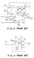
- FIG. 1 shows an example in which plurality of output circuits are connected to a bus line.
- two output terminals of two output circuits such as two try state buffers TB1 and TB1 are connected to s bus line 101, respectively.
- These two try state buffers TB1 and TB2 are both of CMOS structure, which are operative on the basis of two different supply voltages Vcc1 and Vcc2, respectively.
- the try state buffer TB1 becomes active whenever a low level enable signal /EN1 is inputted thereto, and outputs a signal corresponding to a data signal IN1 to the bus line 101.
- the try state buffer TB2 becomes active whenever a low level enable signal /EN2 is inputted thereto, and outputs a signal corresponding to a data signal IN2 to the bus line 101.
- the two try state buffers TB1 and TB2 become inactive, so that the outputs thereof change to a high impedance state, respectively.
- a bus hold circuit 102 is connected to the bus line 101.
- This bus hold circuit 102 of flip-flop mechanism can hold a signal level on the bus line 101 at any one of levels of a supply voltage Vcc and a ground voltage Vss.
- the bus hold circuit 102 is composed of two stages of series-connected inverters IN101 and IN102, and an output terminal of the inverter IN101 and an input terminal of the inverter In102 are connected to the bus line 101, respectively.
- the two inverters IN101 and IN102 are operative on the basis of a supply voltage Vcc different from both the supply voltages Vcc1 and Vcc2 supplied to the two try state buffers TB1 and TB2.
- the potential of the bus line 101 changes to either one of logical [1] or [0] level. This level is held by the bus hold circuit 102. Further, after the two try state buffers TB1 and TB2 have been changed to a high impedance state, respectively, the level of the bus line 101 can be kept held by this bus hold circuit 102. Accordingly, after the two try state buffers TB1 and TB2 have been changed to a high impedance state, respectively, it is possible to prevent the potential level of the bus line 101 from fluctuating due to noise or leak current.
- the bus hold circuit 102 is provided to hold the logical level of the bus line 101, the driving power of the bus hold circuit 102 is determined low enough not to exert a harmful influence upon the operation of the try state buffers TB1 and TB2 for driving the bus line 101.
- the try state buffers are constructed as being of CMOS structure, a P-channel MOS transistor and an N-channel MOS transistor are to be arranged on the output stage thereof.
- a P-type drain diffusion layer of the P-channel transistor is connected to the output terminal of the try state buffer, so that a parasitic pn junction diode is inevitably formed between the output terminal of the try state buffer and a back gate of the P-channel transistor.
- the try state buffer TB2 outputs a signal having a level equal to the supply voltage Vcc2 to the output line 101, if the relationship as Vcc1 + Vf ⁇ Vcc2 can be established, where Vf is a built-in voltage of the parasitic pn junction formed between the output terminal of the try state buffer TB2 and the drain diffusion layer of the P-channel transistor of the output stage, the parasitic diode is biased in the forward direction. As a result, unnecessary current flows from supply voltage (Vcc2) terminal to the supply voltage (Vcc1) terminal via the parasitic diode.
- Fig. 4 shows an example of prior art bus hold circuits.
- an inverter IN102 composed of two series-connected P-channel transistor P101 and N-channel transistor N101 and another inverter IN101 composed of two series-connected P-channel transistor P102 and N-channel transistor N102 are connected in parallel to each other between a supply voltage Vcc and a ground voltage Vss. Further, an input terminal of the inverter IN102 and an output terminal of the inverter IN101 are connected in common to an output terminal Lout connected to a bus line 101.
- the pn junction parasitic diode PND101 is biased in the forward direction.
- unnecessary current flows from the output terminal Lout at the supply voltage Vcc1 or the supply voltage Vcc2 to the supply voltage (Vcc) terminal via this parasitic diode PND101.
- the present invention provides a bus hold circuit, comprising: an input stage inverter connected between a first supply voltage terminal and a second supply voltage terminal and including: a first P-channel transistor; and a first N-channel transistor connected in series to said first P-channel transistor, a gate of said first P-channel transistor and a gate of said first N-channel transistor being connected in common to a bus line; and an output stage inverter also connected between the first supply voltage terminal and the second supply voltage terminal and including: a second P-channel transistor; a third P-channel transistor connected in series to said second P-channel transistor; and a second N-channel transistor connected in series to said third P-channel transistor, a gate of said second P-channel transistor being connected to the bus line, a gate of said third P-channel transistor and a gate of said second N-channel transistor being connected in common to a drain of said first P-channel transistor and a drain of said first N-channel transistor, a drain of said third P-channel transistor and a drain of a drain of
- the second and third P-channel transistors and the second N-channel transistors are connected in series between the first supply voltage and the second supply voltage.
- the back gates of at least the second and third P-channel transistors are connected to the source of the third P-channel transistor, even when a potential higher than the supply voltage is applied to the bus line, since a reverse bias voltage is applied between a parasitic diode formed between source and the back gate of the second P-channel transistor, it is possible to prevent unnecessary current from flowing to the first supply voltage terminal.
- the bus hold circuit it is also preferable to connect the back gate of the first P-channel transistor to the first supply voltage terminal.
- a threshold value of the input stage inverter is set equal to or less than a threshold value of another circuit for receiving signals from the bus line.
- the second and third P-channel transistors are formed in an N-type well different from an N-type well for forming a P-channel transistor included in another circuit connected to the bus line.
- the first, second and third P-channel transistors are all formed in an N-type well formed in a surface of a P-type semiconductor substrate.
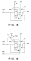
- Fig. 5 shows a first embodiment of the bus hold circuit.
- an inverter IN1 is connected between a supply voltage (Vcc) terminal and a ground voltage (Vss) terminal.
- the inverter IN1 is composed of a P-channel transistor P1 and an N-channel transistor N1 both connected to each other in series.
- An input terminal of this inverter IN1 is connected to an output terminal Lout connected to a bus line (not shown).
- an output terminal L1 of the inverter IN1 is connected to an input terminal of an inverter IN2.
- the inverter IN2 is composed of a P-channel transistor P2 and an N-channel transistor N2. Further, an output terminal of the inverter IN2 is connected to the output terminal Lout.
- a P-channel transistor P3 having a gate connected to a drain thereof is connected between a source of the P-channel transistor P2 of the inverter IN2 and the supply voltage (Vcc) terminal. Further, in parallel to this P-channel transistor P3, a P-channel transistor P4 is connected between the supply voltage (Vcc) terminal and a source of the P-channel transistor P2. A gate of the P-channel transistor P4 is connected to the output terminal Lout.
- the back gates of the P-channel transistors P1 to P4 that is, an N well for forming the transistors P1 to P4 are all connected to the source of the P-channel transistor P2. Further, the back gates of the N-channel transistors N1 and N2 are connected in common to the ground voltage (Vss).
- the voltage Vout of the output terminal Vout can be held in the range as defined by the formula (1).
- the held potential Vout as described above can be recognized as a high level in the input circuit connected to the bus line.
- Vthc the threshold voltage of the input circuit
- Vthc the threshold voltage of the input circuit
- FIG. 6 A second embodiment to the bus hold circuit according to the present invention will be described hereinbelow with reference to Fig. 6.
- This second embodiment is different from the first embodiment shown in Fig. 5 in that an output node L1 of the inverter IN1 is led out as an input signal INA to another input circuit (not shown) and further in that the back gate of the P-channel transistor P1 is connected to the supply voltage (Vcc) terminal.
- the construction other than the above is the same as with the case of the first embodiment, so that the second embodiment operates in the same as with the case of the first embodiment, to hold the potential at the output terminal Lout.
- the feature of this second embodiments reside in that the inverter IN1 is provided with the original function as the initial stage inverter of the bus hold circuit and with the other function as an input stage inverter of another input circuit for receiving the potential outputted to the bus line. Accordingly, the following effects can be obtained:
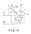
- a third embodiment of the bus hold circuit according to the present invention will be described hereinbelow with reference to Fig. 7.
- the feature of this third embodiment is that a pn junction diode D1 (not a parasitic diode) is additionally formed, by removing the P-channel transistor P3 of the first embodiment shown in Fig. 5.
- Fig. 7 the same reference numerals have been retained for similar elements having the same functions as with the case of the first embodiment, without repeating the similar description thereof.
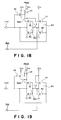
- a fourth embodiment of the bus hold circuit according to the present invention will be described hereinbelow with reference to Fig. 8.
- This fourth embodiment is different from the first embodiment shown in Fig. 5 in that the P-channel transistor P3 is removed.
- the N-type well NW1 can be pulled up by the P-channel transistor P4 and a parasitic pn junction formed between the source and back gate of this P-channel transistor P4.
- the driving capability of pulling up the N-type well NW1 of this fourth embodiment is relatively lower than that of the first embodiment including the P-channel transistor P3 or the second embodiment including the diode D1.
- the back gate of the P-channel transistor P1 can be connected to the supply voltage (Vcc) terminal, as shown in Figs. 9 to 12, respectively, instead of connection to the N-type well NW1.
- Vcc supply voltage
- the P-channel transistor P4 can be removed, as shown in Figs. 13 to 15, respectively.
- the P-channel transistor P4 since the potential of the output terminal Lout is directly inputted to the gate thereof, the sensitivity of the P-channel transistor P4 to the potential change at the terminal Lout is high. Therefore, in order to increase the responsibility to the potential change at the output terminal Lout, it is preferable to provide the P-channel transistor P4 for the bus hold circuit.
- the back gate of the P-channel transistor e.g., the P-channel transistor P201 shown in Fig. 2 or the P-channel transistor P301 shown in Fig. 3 of the try state buffer connected to the bus line is formed in an N-type well different from an N-type well for forming the P-channel transistors of the present invention, in order that the back gate potential of the try state buffer connected to the bus line is not equalized to the back gate potential of the P-channel transistors of the bus hold circuit according to the present invention. This reason is as follows: during the process that the bus line potential rises from the ground potential Vss to the supply voltage potential Vcc by the output circuit, when the potential of the output terminal Lout shown in Fig.
- the P-channel transistor e.g., the P-channel transistor P201 shown in Fig. 2 or the P-channel transistor P301 shown in Fig. 3 of the output stage of the other output circuit which does not drive the bus line is formed on the same N-type well for forming the P-channel transistors of the present invention
- the back gate potential of the P-channel transistor of the output stage of the other output circuit is also pulled down at the same time.
- the P-channel transistor of the output stage of the other output circuit originally deactivated is turned on, so that there exists a problem in that unnecessary current flows to the supply voltage terminal via this turned on P-channel transistor.
- the P-channel transistor of the output stage of the other output circuit on an N-type well electrically separated from the N-type well for forming the P-channel transistors of the bus hold circuit according to the present invention, in such a way that the back gate of the P-channel transistor of the output stage of the other output circuit differs in potential from the back gates of the P-channel transistors of the bus hold circuit according to the present invention.
- the P-channel transistors of the bus hold circuit can be formed on the surface of an N-type well formed on the surface of the P-type semiconductor substrate. Further, the P-channel transistors of the bus hold circuit can be formed in such a way that a deep P-type well is first formed in an N-type semiconductor substrate; an N-type well is formed in the deep P-type well; and the P-channel transistors are formed in the N-type well formed in the deep P-type well, in sequence.
Landscapes
- Engineering & Computer Science (AREA)
- Computer Hardware Design (AREA)
- Physics & Mathematics (AREA)
- Computing Systems (AREA)
- General Engineering & Computer Science (AREA)
- Mathematical Physics (AREA)
- Logic Circuits (AREA)
- Semiconductor Integrated Circuits (AREA)
- Small-Scale Networks (AREA)
- Metal-Oxide And Bipolar Metal-Oxide Semiconductor Integrated Circuits (AREA)
- Electronic Switches (AREA)
Applications Claiming Priority (3)
| Application Number | Priority Date | Filing Date | Title |
|---|---|---|---|
| JP224218/95 | 1995-08-31 | ||
| JP22421895A JP3192937B2 (ja) | 1995-08-31 | 1995-08-31 | バスホールド回路 |
| JP22421895 | 1995-08-31 |
Publications (3)
| Publication Number | Publication Date |
|---|---|
| EP0762648A2 true EP0762648A2 (fr) | 1997-03-12 |
| EP0762648A3 EP0762648A3 (fr) | 1999-01-27 |
| EP0762648B1 EP0762648B1 (fr) | 2003-10-22 |
Family
ID=16810372
Family Applications (1)
| Application Number | Title | Priority Date | Filing Date |
|---|---|---|---|
| EP96113838A Expired - Lifetime EP0762648B1 (fr) | 1995-08-31 | 1996-08-29 | Circuit de maintien de bus |
Country Status (6)
| Country | Link |
|---|---|
| US (1) | US5739702A (fr) |
| EP (1) | EP0762648B1 (fr) |
| JP (1) | JP3192937B2 (fr) |
| KR (1) | KR100241201B1 (fr) |
| DE (1) | DE69630427T2 (fr) |
| TW (1) | TW305956B (fr) |
Cited By (1)
| Publication number | Priority date | Publication date | Assignee | Title |
|---|---|---|---|---|
| FR3062920A1 (fr) * | 2017-02-16 | 2018-08-17 | Spryngs | Circuit de polarisation active et faible consommation d'une entree haute impedance |
Families Citing this family (8)
| Publication number | Priority date | Publication date | Assignee | Title |
|---|---|---|---|---|
| JPH11317657A (ja) | 1998-05-06 | 1999-11-16 | Toshiba Corp | トランスミッション・ゲート回路 |
| TW511335B (en) | 1998-06-09 | 2002-11-21 | Mitsubishi Electric Corp | Integrated circuit |
| US6191607B1 (en) * | 1998-09-16 | 2001-02-20 | Cypress Semiconductor Corporation | Programmable bus hold circuit and method of using the same |
| JP4119062B2 (ja) * | 1999-10-25 | 2008-07-16 | 日本テキサス・インスツルメンツ株式会社 | 終端回路 |
| US6512406B1 (en) * | 1999-12-16 | 2003-01-28 | Intel Corporation | Backgate biased synchronizing latch |
| US6504401B1 (en) * | 2001-11-30 | 2003-01-07 | Xilinx, Inc. | Configurable bus hold circuit with low leakage current |
| US7064593B2 (en) * | 2004-09-20 | 2006-06-20 | Texas Instruments Incorporated | Bus-hold circuit |
| JP4768642B2 (ja) * | 2007-01-17 | 2011-09-07 | エヌイーシーコンピュータテクノ株式会社 | トライステートバス回路 |
Citations (3)
| Publication number | Priority date | Publication date | Assignee | Title |
|---|---|---|---|---|
| DE2929450A1 (de) * | 1978-07-20 | 1980-03-20 | Nippon Electric Co | Schnelle transistorschaltung mit geringer leistungsaufnahme |
| US4484088A (en) * | 1983-02-04 | 1984-11-20 | General Electric Company | CMOS Four-transistor reset/set latch |
| US4558237A (en) * | 1984-03-30 | 1985-12-10 | Honeywell Inc. | Logic families interface circuit and having a CMOS latch for controlling hysteresis |
Family Cites Families (7)
| Publication number | Priority date | Publication date | Assignee | Title |
|---|---|---|---|---|
| US5498976A (en) * | 1990-10-26 | 1996-03-12 | Acer Incorporated | Parallel buffer/driver configuration between data sending terminal and data receiving terminal |
| JPH073958B2 (ja) * | 1992-01-31 | 1995-01-18 | インターナショナル・ビジネス・マシーンズ・コーポレイション | 終端回路 |
| JPH0685653A (ja) * | 1992-05-06 | 1994-03-25 | Sgs Thomson Microelectron Inc | バスキーパ特徴を有するレシーバ回路 |
| US5227677A (en) * | 1992-06-10 | 1993-07-13 | International Business Machines Corporation | Zero power transmission line terminator |
| US5347177A (en) * | 1993-01-14 | 1994-09-13 | Lipp Robert J | System for interconnecting VLSI circuits with transmission line characteristics |
| US5469473A (en) * | 1994-04-15 | 1995-11-21 | Texas Instruments Incorporated | Transceiver circuit with transition detection |
| JP3625881B2 (ja) * | 1994-12-20 | 2005-03-02 | 株式会社ルネサステクノロジ | バスシステム及びバスセンスアンプ |
-
1995
- 1995-08-31 JP JP22421895A patent/JP3192937B2/ja not_active Expired - Fee Related
-
1996
- 1996-08-29 DE DE69630427T patent/DE69630427T2/de not_active Expired - Lifetime
- 1996-08-29 EP EP96113838A patent/EP0762648B1/fr not_active Expired - Lifetime
- 1996-08-29 US US08/704,995 patent/US5739702A/en not_active Expired - Lifetime
- 1996-08-30 KR KR1019960036655A patent/KR100241201B1/ko active IP Right Grant
- 1996-09-19 TW TW085111475A patent/TW305956B/zh not_active IP Right Cessation
Patent Citations (3)
| Publication number | Priority date | Publication date | Assignee | Title |
|---|---|---|---|---|
| DE2929450A1 (de) * | 1978-07-20 | 1980-03-20 | Nippon Electric Co | Schnelle transistorschaltung mit geringer leistungsaufnahme |
| US4484088A (en) * | 1983-02-04 | 1984-11-20 | General Electric Company | CMOS Four-transistor reset/set latch |
| US4558237A (en) * | 1984-03-30 | 1985-12-10 | Honeywell Inc. | Logic families interface circuit and having a CMOS latch for controlling hysteresis |
Cited By (3)
| Publication number | Priority date | Publication date | Assignee | Title |
|---|---|---|---|---|
| FR3062920A1 (fr) * | 2017-02-16 | 2018-08-17 | Spryngs | Circuit de polarisation active et faible consommation d'une entree haute impedance |
| WO2018150111A1 (fr) * | 2017-02-16 | 2018-08-23 | Spryngs | Circuit de polarisation active et faible consommation d'une entrée haute impédance |
| US10931281B2 (en) | 2017-02-16 | 2021-02-23 | Spryngs | Low-power active bias circuit for a high impedance input |
Also Published As
| Publication number | Publication date |
|---|---|
| US5739702A (en) | 1998-04-14 |
| JPH0969770A (ja) | 1997-03-11 |
| DE69630427D1 (de) | 2003-11-27 |
| EP0762648A3 (fr) | 1999-01-27 |
| KR100241201B1 (ko) | 2000-02-01 |
| TW305956B (fr) | 1997-05-21 |
| EP0762648B1 (fr) | 2003-10-22 |
| KR970013701A (ko) | 1997-03-29 |
| JP3192937B2 (ja) | 2001-07-30 |
| DE69630427T2 (de) | 2004-07-29 |
Similar Documents
| Publication | Publication Date | Title |
|---|---|---|
| US5742183A (en) | Level shift semiconductor device | |
| EP0908005B1 (fr) | Amplificateur differentiel | |
| JP3796034B2 (ja) | レベル変換回路および半導体集積回路装置 | |
| US6433586B2 (en) | Semiconductor logic circuit device of low current consumption | |
| EP0410473B1 (fr) | Circuit intégré semi-conducteur | |
| US6801064B1 (en) | Buffer circuit using low voltage transistors and level shifters | |
| EP0614279A2 (fr) | Circuit tampon de sortie tolérant les surtensions | |
| US6791391B2 (en) | Level shifting circuit | |
| KR19980081498A (ko) | Mos 논리회로 및 그 mos 논리회로를 포함하는 반도체장치 | |
| US10181854B1 (en) | Low power input buffer using flipped gate MOS | |
| JP2516302B2 (ja) | 差動受信機 | |
| US5371419A (en) | CMOS well switching circuit | |
| US5880617A (en) | Level conversion circuit and semiconductor integrated circuit | |
| US5739702A (en) | Bus hold circuit | |
| JP4021395B2 (ja) | レベルシフト回路及びそのレベルシフト回路を有する半導体集積回路 | |
| KR20040002722A (ko) | 레벨 시프터, 반도체 집적 회로 및 정보 처리 시스템 | |
| US6624678B1 (en) | Schmitt trigger device with disable | |
| JP3940743B2 (ja) | 半導体集積回路装置およびレベル変換回路 | |
| KR100300687B1 (ko) | 반도체집적회로 | |
| US20090167369A1 (en) | Lvds output driver | |
| US6489815B2 (en) | Low-noise buffer circuit that suppresses current variation | |
| EP0448269A2 (fr) | Circuit d'interface disposé entre un circuit logique à semi-conducteurs composés et un circuit à transistors bipolaires | |
| JP3165751B2 (ja) | 半導体集積回路装置 | |
| JPH11355116A (ja) | Cmos出力バッファ保護回路を有する集積回路 | |
| JP2795046B2 (ja) | 出力バッファ回路 |
Legal Events
| Date | Code | Title | Description |
|---|---|---|---|
| PUAI | Public reference made under article 153(3) epc to a published international application that has entered the european phase |
Free format text: ORIGINAL CODE: 0009012 |
|
| 17P | Request for examination filed |
Effective date: 19960829 |
|
| AK | Designated contracting states |
Kind code of ref document: A2 Designated state(s): DE FR GB IT |
|
| PUAL | Search report despatched |
Free format text: ORIGINAL CODE: 0009013 |
|
| AK | Designated contracting states |
Kind code of ref document: A3 Designated state(s): DE FR GB IT |
|
| 17Q | First examination report despatched |
Effective date: 20020802 |
|
| GRAH | Despatch of communication of intention to grant a patent |
Free format text: ORIGINAL CODE: EPIDOS IGRA |
|
| GRAS | Grant fee paid |
Free format text: ORIGINAL CODE: EPIDOSNIGR3 |
|
| GRAA | (expected) grant |
Free format text: ORIGINAL CODE: 0009210 |
|
| AK | Designated contracting states |
Kind code of ref document: B1 Designated state(s): DE FR GB IT |
|
| REG | Reference to a national code |
Ref country code: GB Ref legal event code: FG4D |
|
| REF | Corresponds to: |
Ref document number: 69630427 Country of ref document: DE Date of ref document: 20031127 Kind code of ref document: P |
|
| ET | Fr: translation filed | ||
| PLBE | No opposition filed within time limit |
Free format text: ORIGINAL CODE: 0009261 |
|
| STAA | Information on the status of an ep patent application or granted ep patent |
Free format text: STATUS: NO OPPOSITION FILED WITHIN TIME LIMIT |
|
| 26N | No opposition filed |
Effective date: 20040723 |
|
| REG | Reference to a national code |
Ref country code: FR Ref legal event code: PLFP Year of fee payment: 20 |
|
| PGFP | Annual fee paid to national office [announced via postgrant information from national office to epo] |
Ref country code: GB Payment date: 20150826 Year of fee payment: 20 Ref country code: DE Payment date: 20150825 Year of fee payment: 20 |
|
| PGFP | Annual fee paid to national office [announced via postgrant information from national office to epo] |
Ref country code: FR Payment date: 20150629 Year of fee payment: 20 |
|
| PGFP | Annual fee paid to national office [announced via postgrant information from national office to epo] |
Ref country code: IT Payment date: 20150827 Year of fee payment: 20 |
|
| REG | Reference to a national code |
Ref country code: DE Ref legal event code: R071 Ref document number: 69630427 Country of ref document: DE |
|
| REG | Reference to a national code |
Ref country code: GB Ref legal event code: PE20 Expiry date: 20160828 |
|
| PG25 | Lapsed in a contracting state [announced via postgrant information from national office to epo] |
Ref country code: GB Free format text: LAPSE BECAUSE OF EXPIRATION OF PROTECTION Effective date: 20160828 |