EP0614279A2 - Circuit tampon de sortie tolérant les surtensions - Google Patents
Circuit tampon de sortie tolérant les surtensions Download PDFInfo
- Publication number
- EP0614279A2 EP0614279A2 EP94300612A EP94300612A EP0614279A2 EP 0614279 A2 EP0614279 A2 EP 0614279A2 EP 94300612 A EP94300612 A EP 94300612A EP 94300612 A EP94300612 A EP 94300612A EP 0614279 A2 EP0614279 A2 EP 0614279A2
- Authority
- EP
- European Patent Office
- Prior art keywords
- output
- transistor
- vout
- coupled
- pseudorail
- Prior art date
- Legal status (The legal status is an assumption and is not a legal conclusion. Google has not performed a legal analysis and makes no representation as to the accuracy of the status listed.)
- Granted
Links
Images
Classifications
-
- H—ELECTRICITY
- H03—ELECTRONIC CIRCUITRY
- H03K—PULSE TECHNIQUE
- H03K19/00—Logic circuits, i.e. having at least two inputs acting on one output; Inverting circuits
- H03K19/02—Logic circuits, i.e. having at least two inputs acting on one output; Inverting circuits using specified components
- H03K19/08—Logic circuits, i.e. having at least two inputs acting on one output; Inverting circuits using specified components using semiconductor devices
- H03K19/094—Logic circuits, i.e. having at least two inputs acting on one output; Inverting circuits using specified components using semiconductor devices using field-effect transistors
- H03K19/09425—Multistate logic
- H03K19/09429—Multistate logic one of the states being the high impedance or floating state
-
- H—ELECTRICITY
- H02—GENERATION; CONVERSION OR DISTRIBUTION OF ELECTRIC POWER
- H02M—APPARATUS FOR CONVERSION BETWEEN AC AND AC, BETWEEN AC AND DC, OR BETWEEN DC AND DC, AND FOR USE WITH MAINS OR SIMILAR POWER SUPPLY SYSTEMS; CONVERSION OF DC OR AC INPUT POWER INTO SURGE OUTPUT POWER; CONTROL OR REGULATION THEREOF
- H02M1/00—Details of apparatus for conversion
- H02M1/32—Means for protecting converters other than automatic disconnection
-
- H—ELECTRICITY
- H02—GENERATION; CONVERSION OR DISTRIBUTION OF ELECTRIC POWER
- H02M—APPARATUS FOR CONVERSION BETWEEN AC AND AC, BETWEEN AC AND DC, OR BETWEEN DC AND DC, AND FOR USE WITH MAINS OR SIMILAR POWER SUPPLY SYSTEMS; CONVERSION OF DC OR AC INPUT POWER INTO SURGE OUTPUT POWER; CONTROL OR REGULATION THEREOF
- H02M1/00—Details of apparatus for conversion
-
- H—ELECTRICITY
- H03—ELECTRONIC CIRCUITRY
- H03K—PULSE TECHNIQUE
- H03K19/00—Logic circuits, i.e. having at least two inputs acting on one output; Inverting circuits
- H03K19/003—Modifications for increasing the reliability for protection
- H03K19/00315—Modifications for increasing the reliability for protection in field-effect transistor circuits
-
- H—ELECTRICITY
- H03—ELECTRONIC CIRCUITRY
- H03K—PULSE TECHNIQUE
- H03K19/00—Logic circuits, i.e. having at least two inputs acting on one output; Inverting circuits
- H03K19/01—Modifications for accelerating switching
- H03K19/017—Modifications for accelerating switching in field-effect transistor circuits
- H03K19/01707—Modifications for accelerating switching in field-effect transistor circuits in asynchronous circuits
- H03K19/01721—Modifications for accelerating switching in field-effect transistor circuits in asynchronous circuits by means of a pull-up or down element
-
- H—ELECTRICITY
- H03—ELECTRONIC CIRCUITRY
- H03K—PULSE TECHNIQUE
- H03K2217/00—Indexing scheme related to electronic switching or gating, i.e. not by contact-making or -breaking covered by H03K17/00
- H03K2217/0018—Special modifications or use of the back gate voltage of a FET
-
- Y—GENERAL TAGGING OF NEW TECHNOLOGICAL DEVELOPMENTS; GENERAL TAGGING OF CROSS-SECTIONAL TECHNOLOGIES SPANNING OVER SEVERAL SECTIONS OF THE IPC; TECHNICAL SUBJECTS COVERED BY FORMER USPC CROSS-REFERENCE ART COLLECTIONS [XRACs] AND DIGESTS
- Y02—TECHNOLOGIES OR APPLICATIONS FOR MITIGATION OR ADAPTATION AGAINST CLIMATE CHANGE
- Y02E—REDUCTION OF GREENHOUSE GAS [GHG] EMISSIONS, RELATED TO ENERGY GENERATION, TRANSMISSION OR DISTRIBUTION
- Y02E10/00—Energy generation through renewable energy sources
- Y02E10/50—Photovoltaic [PV] energy
- Y02E10/56—Power conversion systems, e.g. maximum power point trackers
Definitions
- This invention relates to a new tristate output buffer circuit applicable for multiple output buffer circuit systems driving a common external bus.
- the invention permits multiple output buffer circuits with multiple incompatible power supplies to operate on the common external bus.
- the invention provides overvoltage protection for output driver circuits operating with the new JEDEC Standard 8-1A 3.3v power supply from 5 volt signals applied on the common bus by output buffer circuits operating with JEDEC standard 18 and 20 5v power supplies.
- the protected tristate output buffer circuit of the present invention is particularly applicable for use in notebook, note pad, and personal digital assistant personal computers that utilize the new 3.3v power supply standard but which must also operate with peripheral equipment that utilizes the 5v standard power supply.
- JEDEC Joint Electron Device Engineering Council
- EIA Electronic Industries Association
- the P channel or PMOS transistors are formed with P+ source and drain regions formed in an NWELL which is in turn formed in a grounded P type substrate.
- the NWELL of a PMOS output pullup transistor of the output buffer circuit is coupled to the high potential power rail VCC. If a standard output buffer circuit supplied by the new 3.3v standard power supply has a 5v signal applied to its output from the common external bus, the PN junction between the P+ drain and NWELL will forward bias. This creates a low impedance path from the 5v common external bus, to the internal 3.3v power rail with disruptive effects. It is therefore generally not allowed to have on a common external bus multiple tristate output buffer circuits with incompatible power supplies.
- Another object of the invention is to provide a new overvoltage tolerant tristate output buffer circuit with increased protection and isolation of a lower voltage internal power supply rail such as a 3.3v standard power supply rail from overvoltage signals such as 5v signals on internal nodes of the output buffer circuit.
- a more specific object of the invention is to provide an overvoltage tolerant tristate output buffer circuit with pullup enhancement circuits to improve turn off of a PMOS output pullup transistor and turn on of an NMOS output pulldown transistor.
- the invention broadly provides a tristate output buffer circuit having a data input for receiving input signals of logic high and low potential levels, an output pullup transistor coupled between an output and a high potential power rail and an output pulldown transistor potential coupled between the output and a low potential power rail for driving output signals on a common bus, said tristate output buffer circuit having a tristate enable input for implementing a tristate operating mode at the output, characterised by, for tolerating overvoltage greater than the high potential power rail voltage level at the output: a high potential level pseudorail coupled to the output pullup transistor; and a comparator circuit coupling the pseudorail to the output, said comparator circuit comprising means for coupling the pseudorail to the high potential power rail if the voltage level at the output is less than the voltage level of the high potential power rail and to couple the pseudorail to the output if the voltage level at the output is greater than the voltage level of the high potential power rail.
- the invention provides a high potential level pseudorail coupled at the NWELL of a P channel output pullup transistor.
- a comparator circuit couples the pseudorail to the output.
- the comparator circuit includes passgates constructed to couple the pseudorail to the high potential power rail if the voltage level at the output is less than the voltage level of the high potential power rail (VOUT ⁇ VCC).
- the passgates also couple the pseudorail to the output if the voltage level at the output is greater than the voltage level of the high potential power rail (VOUT > VCC).
- a feedback transistor couples the pseudorail to an internal node of the tristate buffer circuit at the control gate node of the output pullup transistor.
- the feedback transistor has a control gate node coupled to a tristate enable input for turning on the feedback transistor during the tristate operating mode and holding off the output pullup transistor.
- At least one N channel pullup transistor is coupled between the control gate node of the output pullup transistor and the high potential power rail to isolate overvoltage signals at the internal node from the high potential power rail.
- a first N channel pullup transistor has a control gate node coupled to the input.
- the N channel pullup transistors are selected to have a relatively small turn on threshold voltage VTN less than the absolute value of the turn on voltage threshold VTP of the P channel output pullup transistor, i.e. VTN ⁇ [VTP].
- the selection of N channel transistors enhances turn off of the output pullup transistor when driving a low potential level signal at the output.
- the new tristate output buffer circuit also includes a pulldown enhancement circuit coupled between the pseudorail and a control gate node of the output pulldown transistor.
- the pulldown enhancement circuit pulls up the control gate node to the potential level of the pseudorail when driving a logic low potential level signal at the output.
- a first N channel pullup transistor coupled between the high potential power rail and control gate node of the output pullup transistor has a control gate node coupled to the input of the tristate output buffer circuit.
- a second N channel pullup transistor has a control gate node coupled to a complementary tristate enable input.
- a third N channel transistor is coupled to the feedback transistor in an inverter stage. The inverter stage has an input coupled to the tristate enable input and an output coupled to the control gate node of the output pullup transistor for implementing the tristate operating mode.
- the third N channel transistor has a source coupled to the control gate node of the output pulldown transistor to isolate an overvoltage signal at the control gate node from the high potential power rail.
- All three N channel transistors are selected to have a turn on voltage threshold VTN less than the absolute value of the turn on voltage threshold VTP of the PMOS output pullup transistor.
- VTN may be reduced by utilizing an additional threshold adjust step during processing to create a set of low VTN devices with VTN ⁇
- the comparator circuit includes a first P channel passgate coupled between the pseudorail and output having a control gate node coupled to the high potential power rail.
- the first passgate passes the voltage level at the output to the pseudorail when the voltage level at the output is greater than the high potential power rail voltage level (VOUT > VCC).
- a second P channel passgate is coupled between the high potential power rail and pseudorail and has a control gate node coupled to the output.
- the second passgate passes the high potential power rail voltage level to the pseudorail when the voltage level at the output is less than the high potential power rail voltage level (VOUT ⁇ VCC).
- the first and second P channel passgates have NWELL's or backgates coupled to the output.
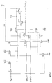
- Figure 1 is a schematic circuit diagram of a new tristate output buffer circuit with overvoltage protection according to the invention.
- a tristate output buffer circuit 10 with overvoltage protection is illustrated in Fig; 1.
- Data signals of logic high and low potential levels are applied at the input V IN for driving output signals at the output VOUT.
- the output VOUT is coupled to a common external bus with other tristate output buffer circuits.
- Input signals are divided into a pullup circuit path through a pullup predriver inverter stage I1, and into a pulldown circuit path through pulldown predriver inverting transistor N4.
- a PMOS output pullup transistor P4 is coupled between the internal high potential power rail VCC and the output VOUT for sourcing current from a 3.3v standard power supply VCC to the output VOUT during the normal bistate operating mode.
- An NMOS output pulldown transistor N6 is coupled between the output VOUT and low potential power rail GND for sinking current from the output during the normal bistate operating mode.
- the output buffer circuit also incorporates tristate enable circuitry with complementary tristate enable inputs EN and ENB.
- the complementary tristate enable inputs EN and DNB are coupled to tristate implementing transistors N2,N3, and N5 for implementing the high impedance third state at the output VOUT.
- the complementary tristate enable signal inputs EN,ENB are also coupled to two additional PMOS transistors P1,P3 which perform other novel circuit functions as hereafter described.
- the tristate output buffer circuit 10 is provided with a high potential pseudorail PV coupled to the NWELL of the P channel output pullup transistor P4.
- a comparator circuit P5,P6 is coupled between the pseudorail PV and output VOUT.
- the comparator circuit consists of a first PMOS transistor passgate P6 coupled between the pseudorail PV and output VOUT.
- the gate node of passgate P6 is coupled to the internal high potential power rail VCC at 3.3v. Therefore if a voltage signal appears at the output VOUT having a voltage level greater than VCC, that is, greater than approximately 3.3v ⁇ 0.3v, for example a 5 volt signal driven by a 5v standard tristate output buffer circuit on the common external bus, the passgate P6 becomes conducting and applies its drain voltage level to the pseudorail PV.
- PV VOUT.
- the second PMOS transistor passgate P5 is coupled between the pseudorail PV and internal high potential power rail VCC.
- the gate node of passgate P5 is coupled to the output VOUT. Therefore, for voltage signals at the output VOUT having a voltage level less than VCC, passgate P6 is held off while passgate P5 becomes conducting.
- Passgate P5 applies the internal high potential power rail voltage level of nominal 3.3v with an actual range of approximately 3.3v ⁇ 0.3v, to the pseudorail PV.
- VOUT ⁇ VCC VCC.
- VCC VCC
- the pseudorail PV is in a high impedance Z condition.
- the NWELL's or backgates of the P channel passgate transistors P5 and P6 are both connected to PV.
- the NWELL voltage therefore coincides with the source voltages to prevent forward biasing of leakage current paths from an overvoltage signal at the output VOUT to the internal high potential power rail VCC.
- the pseudorail PV is also coupled to an internal node of the output buffer circuit namely the control gate node of output pullup transistor P4 through PMOS feedback transistor P1.
- the control gate node of feedback transistor P1 is coupled to the tristate enable input EN.
- feedback transistor P1 applies the high potential level 5 volt signal to the gate node holding off PMOS output pullup transistor P4.
- the tristate enable signal input EN is low while the complementary tristate enable signal input ENB is high.
- the inverter gate formed by transistors P1/N3 then holds off the output pullup transistor P4. At the same time tristate transistor N5 discharges and holds off the output pulldown transistor N6.
- N channel transistors N1 and N2 instead of conventional P channel pullup transistors.
- N channel pullup transistor N1 prevents the internal power rail VCC from being charged above VCC by the 5 volt signal applied to the gate of P4.
- similarly tristate pullup transistor N2 is an N channel transistor for isolating the internal power supply rail VCC from an overvoltage signal at the internal node.
- N channel pullup transistors N1 and N2 are therefore fabricated in a CMOS fabricating process which yields N channel pullup transistors N1,N2 having a relatively small turn on voltage threshold VTN less than the absolute value of the turn on threshold voltage VTP of the output pullup transistor P4.
- can also be satisfied by utilizing an additional threshold adjust step to create a set of low VT transistors for the N channel pullup transistors N1,N2. In either case VTN can be reduced from a conventional 0.85v to for example 0.5-0.6v. This condition enhances the pullup and turn off of output pullup transistor P4.
- transistor N3 in the normal bistate operating mode with tristate enable input EN high and complementary tristate enable input ENB low provides only degraded pullup of the pulldown transistor N6.
- Limitation on the pullup of the voltage at the control gate node of N6 limits turn on of the output pulldown transistor N6 for rapid sinking and discharge of current from the output VOUT.
- This problem is alleviated by selecting the third N channel transistor N3 also to have a relatively small turn on voltage threshold VTN or by selecting tristate transistor N3 also to be a low VT type N channel transistor.
- the low VT type N channel transistor symbol is indicated for NMOS transistors N1,N2, and N3 by the extra line in the transistor symbol.
- an output pulldown transistor pullup enhancement circuit 12 is coupled between the pseudorail PV and control gate node of the output pulldown transistor N6.
- Pullup enhancement circuit 12 for restoring control gate node voltage to the high potential power rail voltage level is accomplished by two PMOS transistors P2 and P3 coupled in series between the pseudorail PV and control gate node.
- the gate node of PMOS transistor P2 is coupled to the output while the gate node of PMOS transistor P3 is coupled to the complementary tristate enable input ENB.
- both enhancement circuit transistors P2 and P3 are conducting pulling up the gate node of output pulldown transistor N6 to the voltage level of pseudorail PV which equals VCC.
- the NWELL's of pullup enhancement transistors P2 and P3 can be tied to the pseudorail PV.
- the pullup enhancement circuit 12 is an optional circuit and may be omitted from the output buffer circuit.
- tristate transistor N3 also performs an isolation function isolating the overvoltage signal at the output pulldown transistor gate node from other internal nodes of the tristate output transistor and more importantly the internal high potential power rail.
- pulldown transistors N4 and N5 hold off output pulldown N6 and through tristate transistor N3 turn on output pullup transistor P4 when driving a high potential level signal at the output.
Applications Claiming Priority (2)
| Application Number | Priority Date | Filing Date | Title |
|---|---|---|---|
| US24942 | 1993-03-02 | ||
| US08/024,942 US5381061A (en) | 1993-03-02 | 1993-03-02 | Overvoltage tolerant output buffer circuit |
Publications (3)
| Publication Number | Publication Date |
|---|---|
| EP0614279A2 true EP0614279A2 (fr) | 1994-09-07 |
| EP0614279A3 EP0614279A3 (fr) | 1995-01-04 |
| EP0614279B1 EP0614279B1 (fr) | 1998-08-26 |
Family
ID=21823162
Family Applications (1)
| Application Number | Title | Priority Date | Filing Date |
|---|---|---|---|
| EP94300612A Expired - Lifetime EP0614279B1 (fr) | 1993-03-02 | 1994-01-27 | Circuit tampon de sortie tolérant les surtensions |
Country Status (5)
| Country | Link |
|---|---|
| US (1) | US5381061A (fr) |
| EP (1) | EP0614279B1 (fr) |
| JP (1) | JP3100824B2 (fr) |
| KR (1) | KR100294254B1 (fr) |
| DE (1) | DE69412667T2 (fr) |
Cited By (11)
| Publication number | Priority date | Publication date | Assignee | Title |
|---|---|---|---|---|
| EP0706267A2 (fr) * | 1994-10-05 | 1996-04-10 | Pericom Semiconductor Corp. | Tampon de sortie à Haute impédance entièrement CMOS pour bus commandé par de multiple tensions d'alimentation |
| FR2730107A1 (fr) * | 1995-01-31 | 1996-08-02 | Cypress Semiconductor Corp | Tampon de sortie de circuit integre tolerant aux surtensions |
| WO1997021272A1 (fr) * | 1995-12-01 | 1997-06-12 | Philips Electronics N.V. | Circuit comportant un conducteur de type bus et circuit d'interface avec ledit bus |
| EP0848498A1 (fr) * | 1996-12-10 | 1998-06-17 | Fujitsu Limited | Circuit tampon de sortie dans un dispositif semi-conducteur |
| DE19710488A1 (de) * | 1996-11-27 | 1998-06-18 | Lg Semicon Co Ltd | Gegen 5V widerstandsfähige Eingangs-/Ausgangsschaltung |
| EP0851555A2 (fr) * | 1996-12-31 | 1998-07-01 | STMicroelectronics, Inc. | Circuit intégré avec protection améliorée contre des surcharges |
| EP0874462A1 (fr) * | 1997-04-25 | 1998-10-28 | Fujitsu Limited | Circuit de tirage vers le haut et dispositif semi-conducteur en fasisant usage |
| EP0902517A2 (fr) * | 1997-09-09 | 1999-03-17 | Motorola, Inc. | Circuit comportant une protection contre les électrons chauds |
| US6225846B1 (en) * | 1997-01-23 | 2001-05-01 | Mitsubishi Denki Kabushiki Kaisha | Body voltage controlled semiconductor integrated circuit |
| CN1116682C (zh) * | 1994-12-29 | 2003-07-30 | 三星电子株式会社 | 半导体存贮器装置的数据输出缓冲电路 |
| EP2503690A3 (fr) * | 2011-03-21 | 2014-02-26 | Nxp B.V. | Circuit de protection contre des courants de retour |
Families Citing this family (32)
| Publication number | Priority date | Publication date | Assignee | Title |
|---|---|---|---|---|
| US5406140A (en) * | 1993-06-07 | 1995-04-11 | National Semiconductor Corporation | Voltage translation and overvoltage protection |
| US5455732A (en) * | 1993-09-15 | 1995-10-03 | National Semiconductor Corporation | Buffer protection against output-node voltage excursions |
| JP3160449B2 (ja) * | 1993-12-02 | 2001-04-25 | 株式会社東芝 | トランジスタ回路 |
| JP3311133B2 (ja) * | 1994-02-16 | 2002-08-05 | 株式会社東芝 | 出力回路 |
| KR0120565B1 (ko) * | 1994-04-18 | 1997-10-30 | 김주용 | 래치-업을 방지한 씨모스형 데이타 출력버퍼 |
| US5467031A (en) * | 1994-09-22 | 1995-11-14 | Lsi Logic Corporation | 3.3 volt CMOS tri-state driver circuit capable of driving common 5 volt line |
| US6040711A (en) * | 1995-03-31 | 2000-03-21 | Sgs-Thomson Microelectronics S.R.L. | CMOS output buffer having a switchable bulk line |
| JP3441238B2 (ja) * | 1995-06-02 | 2003-08-25 | 株式会社東芝 | 出力回路 |
| EP0782269B1 (fr) * | 1995-12-26 | 2002-06-05 | Kabushiki Kaisha Toshiba | Circuit intégré semi-conducteur |
| JP3340906B2 (ja) * | 1996-03-13 | 2002-11-05 | 株式会社 沖マイクロデザイン | 出力回路 |
| US6104229A (en) * | 1996-05-02 | 2000-08-15 | Integrated Device Technology, Inc. | High voltage tolerable input buffer and method for operating same |
| US5844425A (en) * | 1996-07-19 | 1998-12-01 | Quality Semiconductor, Inc. | CMOS tristate output buffer with having overvoltage protection and increased stability against bus voltage variations |
| US5828262A (en) * | 1996-09-30 | 1998-10-27 | Cypress Semiconductor Corp. | Ultra low power pumped n-channel output buffer with self-bootstrap |
| US5894241A (en) * | 1996-09-30 | 1999-04-13 | Cypress Semiconductor Corp. | Bootstrap augmentation circuit and method |
| US5804998A (en) * | 1996-12-26 | 1998-09-08 | International Business Machines Corporation | Voltage upwardly compliant CMOS off-chip driver |
| US5969541A (en) * | 1997-05-19 | 1999-10-19 | Stmicroelectronics, Inc. | Current inhibiting I/O buffer having a 5 volt tolerant input and method of inhibiting current |
| US6049242A (en) | 1997-10-14 | 2000-04-11 | Cypress Semiconductor Corp. | Voltage reference source for an overvoltage-tolerant bus interface |
| US6225819B1 (en) | 1998-03-17 | 2001-05-01 | Cypress Semiconductor Corp. | Transmission line impedance matching output buffer |
| US6150845A (en) * | 1999-06-01 | 2000-11-21 | Fairchild Semiconductor Corp. | Bus hold circuit with overvoltage tolerance |
| US6313661B1 (en) | 2000-03-31 | 2001-11-06 | Intel Corporation | High voltage tolerant I/O buffer |
| US6496054B1 (en) | 2000-05-13 | 2002-12-17 | Cypress Semiconductor Corp. | Control signal generator for an overvoltage-tolerant interface circuit on a low voltage process |
| US6628489B1 (en) * | 2000-05-31 | 2003-09-30 | Integration Associates Inc. | Battery and current reversal protect circuit |
| US6580291B1 (en) | 2000-12-18 | 2003-06-17 | Cypress Semiconductor Corp. | High voltage output buffer using low voltage transistors |
| US6384621B1 (en) | 2001-02-22 | 2002-05-07 | Cypress Semiconductor Corp. | Programmable transmission line impedance matching circuit |
| US6731486B2 (en) | 2001-12-19 | 2004-05-04 | Fairchild Semiconductor Corporation | Output-powered over-voltage protection circuit |
| CN1293703C (zh) * | 2003-11-05 | 2007-01-03 | 中芯国际集成电路制造(上海)有限公司 | 用于高电压输入的上拉晶体管的栅极控制电路 |
| CN100452654C (zh) * | 2003-11-05 | 2009-01-14 | 中芯国际集成电路制造(上海)有限公司 | 用于高电压输入的上拉晶体管的栅极控制电路 |
| US7888962B1 (en) | 2004-07-07 | 2011-02-15 | Cypress Semiconductor Corporation | Impedance matching circuit |
| US8018268B1 (en) | 2004-11-19 | 2011-09-13 | Cypress Semiconductor Corporation | Over-voltage tolerant input circuit |
| US8036846B1 (en) | 2005-10-20 | 2011-10-11 | Cypress Semiconductor Corporation | Variable impedance sense architecture and method |
| US7813093B2 (en) * | 2008-02-15 | 2010-10-12 | Analog Devices, Inc. | Output driver with overvoltage protection |
| CN103427774B (zh) * | 2012-05-24 | 2017-02-01 | 意法半导体研发(深圳)有限公司 | 具有增强的电流吸收能力的运算跨导放大器 |
Citations (1)
| Publication number | Priority date | Publication date | Assignee | Title |
|---|---|---|---|---|
| US5160855A (en) * | 1991-06-28 | 1992-11-03 | Digital Equipment Corporation | Floating-well CMOS output driver |
Family Cites Families (9)
| Publication number | Priority date | Publication date | Assignee | Title |
|---|---|---|---|---|
| JPS61164249A (ja) * | 1985-01-16 | 1986-07-24 | Fujitsu Ltd | 半導体装置 |
| US4670668A (en) * | 1985-05-09 | 1987-06-02 | Advanced Micro Devices, Inc. | Substrate bias generator with power supply control means to sequence application of bias and power to prevent CMOS SCR latch-up |
| US4670861A (en) * | 1985-06-21 | 1987-06-02 | Advanced Micro Devices, Inc. | CMOS N-well bias generator and gating system |
| US4906056A (en) * | 1987-04-14 | 1990-03-06 | Mitsubishi Denki Kabushiki Kaisha | High speed booster circuit |
| US5060044A (en) * | 1987-05-28 | 1991-10-22 | Texas Instruments Incorporated | Integrated bipolar-CMOS circuit isolation for providing different backgate and substrate bias |
| US5004936A (en) * | 1989-03-31 | 1991-04-02 | Texas Instruments Incorporated | Non-loading output driver circuit |
| US5117129A (en) * | 1990-10-16 | 1992-05-26 | International Business Machines Corporation | Cmos off chip driver for fault tolerant cold sparing |
| US5144165A (en) * | 1990-12-14 | 1992-09-01 | International Business Machines Corporation | CMOS off-chip driver circuits |
| US5266849A (en) * | 1992-02-19 | 1993-11-30 | Hal Computer Systems, Inc. | Tri state buffer circuit for dual power system |
-
1993
- 1993-03-02 US US08/024,942 patent/US5381061A/en not_active Expired - Lifetime
-
1994
- 1994-01-27 EP EP94300612A patent/EP0614279B1/fr not_active Expired - Lifetime
- 1994-01-27 DE DE69412667T patent/DE69412667T2/de not_active Expired - Lifetime
- 1994-02-28 KR KR1019940003652A patent/KR100294254B1/ko not_active IP Right Cessation
- 1994-03-02 JP JP06032470A patent/JP3100824B2/ja not_active Expired - Fee Related
Patent Citations (1)
| Publication number | Priority date | Publication date | Assignee | Title |
|---|---|---|---|---|
| US5160855A (en) * | 1991-06-28 | 1992-11-03 | Digital Equipment Corporation | Floating-well CMOS output driver |
Non-Patent Citations (1)
| Title |
|---|
| IBM TECHNICAL DISCLOSURE BULLETIN., vol.24, no.5, October 1981, NEW YORK US pages 2558 - 2559 GRIFFIN 'high speed complementary driver circuit' * |
Cited By (17)
| Publication number | Priority date | Publication date | Assignee | Title |
|---|---|---|---|---|
| EP0706267A3 (fr) * | 1994-10-05 | 1996-09-25 | Pericom Semiconductor Corp | Tampon de sortie à Haute impédance entièrement CMOS pour bus commandé par de multiple tensions d'alimentation |
| EP0706267A2 (fr) * | 1994-10-05 | 1996-04-10 | Pericom Semiconductor Corp. | Tampon de sortie à Haute impédance entièrement CMOS pour bus commandé par de multiple tensions d'alimentation |
| CN1116682C (zh) * | 1994-12-29 | 2003-07-30 | 三星电子株式会社 | 半导体存贮器装置的数据输出缓冲电路 |
| FR2730107A1 (fr) * | 1995-01-31 | 1996-08-02 | Cypress Semiconductor Corp | Tampon de sortie de circuit integre tolerant aux surtensions |
| WO1997021272A1 (fr) * | 1995-12-01 | 1997-06-12 | Philips Electronics N.V. | Circuit comportant un conducteur de type bus et circuit d'interface avec ledit bus |
| DE19710488A1 (de) * | 1996-11-27 | 1998-06-18 | Lg Semicon Co Ltd | Gegen 5V widerstandsfähige Eingangs-/Ausgangsschaltung |
| DE19710488C2 (de) * | 1996-11-27 | 1998-10-08 | Lg Semicon Co Ltd | Gegen 5V widerstandsfähige Eingangs-/Ausgangsschaltung |
| EP0848498A1 (fr) * | 1996-12-10 | 1998-06-17 | Fujitsu Limited | Circuit tampon de sortie dans un dispositif semi-conducteur |
| US5936456A (en) * | 1996-12-10 | 1999-08-10 | Fujitsu Limited | Output driver circuit in semiconductor device |
| EP0851555A2 (fr) * | 1996-12-31 | 1998-07-01 | STMicroelectronics, Inc. | Circuit intégré avec protection améliorée contre des surcharges |
| EP0851555A3 (fr) * | 1996-12-31 | 1999-08-25 | STMicroelectronics, Inc. | Circuit intégré avec protection améliorée contre des surcharges |
| US6225846B1 (en) * | 1997-01-23 | 2001-05-01 | Mitsubishi Denki Kabushiki Kaisha | Body voltage controlled semiconductor integrated circuit |
| EP0874462A1 (fr) * | 1997-04-25 | 1998-10-28 | Fujitsu Limited | Circuit de tirage vers le haut et dispositif semi-conducteur en fasisant usage |
| US5966044A (en) * | 1997-04-25 | 1999-10-12 | Fujitsu Limited | Pull-up circuit and semiconductor device using the same |
| EP0902517A3 (fr) * | 1997-09-09 | 2000-01-12 | Motorola, Inc. | Circuit comportant une protection contre les électrons chauds |
| EP0902517A2 (fr) * | 1997-09-09 | 1999-03-17 | Motorola, Inc. | Circuit comportant une protection contre les électrons chauds |
| EP2503690A3 (fr) * | 2011-03-21 | 2014-02-26 | Nxp B.V. | Circuit de protection contre des courants de retour |
Also Published As
| Publication number | Publication date |
|---|---|
| EP0614279A3 (fr) | 1995-01-04 |
| JPH077411A (ja) | 1995-01-10 |
| KR100294254B1 (ko) | 2001-09-17 |
| JP3100824B2 (ja) | 2000-10-23 |
| KR940022990A (ko) | 1994-10-22 |
| DE69412667T2 (de) | 1999-03-25 |
| US5381061A (en) | 1995-01-10 |
| DE69412667D1 (de) | 1998-10-01 |
| EP0614279B1 (fr) | 1998-08-26 |
Similar Documents
| Publication | Publication Date | Title |
|---|---|---|
| EP0614279B1 (fr) | Circuit tampon de sortie tolérant les surtensions | |
| US5534795A (en) | Voltage translation and overvoltage protection | |
| EP0702860B1 (fr) | Protection contre les surtensions | |
| EP1024597B1 (fr) | Circuit de sortie pour utilisation dans un circuit intégré semi-conducteur | |
| US5321324A (en) | Low-to-high voltage translator with latch-up immunity | |
| KR100298927B1 (ko) | 다중 전원 분리를 지니는 풀 스윙 파워 다운 버퍼 회로 | |
| US5933025A (en) | Low voltage interface circuit with a high voltage tolerance | |
| US6859074B2 (en) | I/O circuit using low voltage transistors which can tolerate high voltages even when power supplies are powered off | |
| US7573304B2 (en) | Input/output circuit and input/output device | |
| US5646809A (en) | High voltage tolerant CMOS input/output pad circuits | |
| US6060906A (en) | Bidirectional buffer with active pull-up/latch circuit for mixed-voltage applications | |
| EP0621692B1 (fr) | Circuit de protection contre les surtensions | |
| US6040729A (en) | Digital output buffer for multiple voltage system | |
| US7477075B2 (en) | CMOS output driver using floating wells to prevent leakage current | |
| US6803789B1 (en) | High voltage tolerant output buffer | |
| US6313672B1 (en) | Over-voltage tolerant integrated circuit I/O buffer | |
| US7230469B2 (en) | Multi-level/single ended input level shifter circuit | |
| EP1032132B1 (fr) | Tampon de sortie pour récepteur différentiel de signalisation basse tension | |
| US6265931B1 (en) | Voltage reference source for an overvoltage-tolerant bus interface | |
| US6496054B1 (en) | Control signal generator for an overvoltage-tolerant interface circuit on a low voltage process | |
| US6064231A (en) | CMOS input buffer protection circuit | |
| US6201428B1 (en) | 5-volt tolerant 3-volt drive push-pull buffer/driver | |
| US20030151428A1 (en) | 5 Volt tolerant input/output buffer | |
| KR19990083515A (ko) | 씨모스출력버퍼보호회로 | |
| Chow | Bidirectional buffer for mixed voltage applications |
Legal Events
| Date | Code | Title | Description |
|---|---|---|---|
| PUAI | Public reference made under article 153(3) epc to a published international application that has entered the european phase |
Free format text: ORIGINAL CODE: 0009012 |
|
| AK | Designated contracting states |
Kind code of ref document: A2 Designated state(s): DE FR GB IT |
|
| PUAL | Search report despatched |
Free format text: ORIGINAL CODE: 0009013 |
|
| AK | Designated contracting states |
Kind code of ref document: A3 Designated state(s): DE FR GB IT |
|
| 17P | Request for examination filed |
Effective date: 19950629 |
|
| 17Q | First examination report despatched |
Effective date: 19961025 |
|
| GRAG | Despatch of communication of intention to grant |
Free format text: ORIGINAL CODE: EPIDOS AGRA |
|
| GRAG | Despatch of communication of intention to grant |
Free format text: ORIGINAL CODE: EPIDOS AGRA |
|
| GRAH | Despatch of communication of intention to grant a patent |
Free format text: ORIGINAL CODE: EPIDOS IGRA |
|
| GRAH | Despatch of communication of intention to grant a patent |
Free format text: ORIGINAL CODE: EPIDOS IGRA |
|
| RAP1 | Party data changed (applicant data changed or rights of an application transferred) |
Owner name: FAIRCHILD SEMICONDUCTOR CORPORATION |
|
| GRAA | (expected) grant |
Free format text: ORIGINAL CODE: 0009210 |
|
| AK | Designated contracting states |
Kind code of ref document: B1 Designated state(s): DE FR GB IT |
|
| PG25 | Lapsed in a contracting state [announced via postgrant information from national office to epo] |
Ref country code: IT Free format text: LAPSE BECAUSE OF FAILURE TO SUBMIT A TRANSLATION OF THE DESCRIPTION OR TO PAY THE FEE WITHIN THE PRE;WARNING: LAPSES OF ITALIAN PATENTS WITH EFFECTIVE DATE BEFORE 2007 MAY HAVE OCCURRED AT ANY TIME BEFORE 2007. THE CORRECT EFFECTIVE DATE MAY BE DIFFERENT FROM THE ONE RECORDED.SCRIBED TIME-LIMIT Effective date: 19980826 Ref country code: FR Free format text: LAPSE BECAUSE OF FAILURE TO SUBMIT A TRANSLATION OF THE DESCRIPTION OR TO PAY THE FEE WITHIN THE PRESCRIBED TIME-LIMIT Effective date: 19980826 |
|
| REF | Corresponds to: |
Ref document number: 69412667 Country of ref document: DE Date of ref document: 19981001 |
|
| EN | Fr: translation not filed | ||
| PG25 | Lapsed in a contracting state [announced via postgrant information from national office to epo] |
Ref country code: GB Free format text: LAPSE BECAUSE OF NON-PAYMENT OF DUE FEES Effective date: 19990127 |
|
| PLBE | No opposition filed within time limit |
Free format text: ORIGINAL CODE: 0009261 |
|
| STAA | Information on the status of an ep patent application or granted ep patent |
Free format text: STATUS: NO OPPOSITION FILED WITHIN TIME LIMIT |
|
| 26N | No opposition filed | ||
| GBPC | Gb: european patent ceased through non-payment of renewal fee |
Effective date: 19990127 |
|
| REG | Reference to a national code |
Ref country code: HK Ref legal event code: WD Ref document number: 1014091 Country of ref document: HK |
|
| PGFP | Annual fee paid to national office [announced via postgrant information from national office to epo] |
Ref country code: DE Payment date: 20110127 Year of fee payment: 18 |
|
| PG25 | Lapsed in a contracting state [announced via postgrant information from national office to epo] |
Ref country code: DE Free format text: LAPSE BECAUSE OF NON-PAYMENT OF DUE FEES Effective date: 20120801 |
|
| REG | Reference to a national code |
Ref country code: DE Ref legal event code: R119 Ref document number: 69412667 Country of ref document: DE Effective date: 20120801 |