EP0761361B1 - Gerät zum Abkühlen von gedruckten Schaltungsplatten beim Wellenlöten - Google Patents
Gerät zum Abkühlen von gedruckten Schaltungsplatten beim Wellenlöten Download PDFInfo
- Publication number
- EP0761361B1 EP0761361B1 EP96306340A EP96306340A EP0761361B1 EP 0761361 B1 EP0761361 B1 EP 0761361B1 EP 96306340 A EP96306340 A EP 96306340A EP 96306340 A EP96306340 A EP 96306340A EP 0761361 B1 EP0761361 B1 EP 0761361B1
- Authority
- EP
- European Patent Office
- Prior art keywords
- distributing
- gas
- distributing manifold
- circuit board
- tunnel
- Prior art date
- Legal status (The legal status is an assumption and is not a legal conclusion. Google has not performed a legal analysis and makes no representation as to the accuracy of the status listed.)
- Expired - Lifetime
Links
- 238000005476 soldering Methods 0.000 title claims description 25
- 238000001816 cooling Methods 0.000 title claims description 18
- 239000007789 gas Substances 0.000 claims description 36
- 229910000679 solder Inorganic materials 0.000 claims description 18
- 239000011261 inert gas Substances 0.000 claims description 8
- 238000009826 distribution Methods 0.000 claims description 7
- 230000003190 augmentative effect Effects 0.000 claims description 3
- 239000002826 coolant Substances 0.000 claims description 2
- 230000003647 oxidation Effects 0.000 claims description 2
- 238000007254 oxidation reaction Methods 0.000 claims description 2
- 238000005057 refrigeration Methods 0.000 claims description 2
- 239000007921 spray Substances 0.000 description 6
- 238000010438 heat treatment Methods 0.000 description 3
- 238000000034 method Methods 0.000 description 3
- XKRFYHLGVUSROY-UHFFFAOYSA-N Argon Chemical compound [Ar] XKRFYHLGVUSROY-UHFFFAOYSA-N 0.000 description 2
- IJGRMHOSHXDMSA-UHFFFAOYSA-N Atomic nitrogen Chemical compound N#N IJGRMHOSHXDMSA-UHFFFAOYSA-N 0.000 description 2
- CURLTUGMZLYLDI-UHFFFAOYSA-N Carbon dioxide Chemical compound O=C=O CURLTUGMZLYLDI-UHFFFAOYSA-N 0.000 description 2
- 230000004907 flux Effects 0.000 description 2
- 230000008569 process Effects 0.000 description 2
- 230000001681 protective effect Effects 0.000 description 2
- 230000001154 acute effect Effects 0.000 description 1
- 229910045601 alloy Inorganic materials 0.000 description 1
- 239000000956 alloy Substances 0.000 description 1
- 238000013459 approach Methods 0.000 description 1
- 229910052786 argon Inorganic materials 0.000 description 1
- 230000004888 barrier function Effects 0.000 description 1
- 239000001569 carbon dioxide Substances 0.000 description 1
- 229910002092 carbon dioxide Inorganic materials 0.000 description 1
- 238000004140 cleaning Methods 0.000 description 1
- 230000007613 environmental effect Effects 0.000 description 1
- 239000012530 fluid Substances 0.000 description 1
- 230000006872 improvement Effects 0.000 description 1
- 238000013101 initial test Methods 0.000 description 1
- 238000009413 insulation Methods 0.000 description 1
- 238000004519 manufacturing process Methods 0.000 description 1
- 239000000155 melt Substances 0.000 description 1
- 230000005012 migration Effects 0.000 description 1
- 238000013508 migration Methods 0.000 description 1
- 229910052757 nitrogen Inorganic materials 0.000 description 1
- 230000001737 promoting effect Effects 0.000 description 1
- 238000000926 separation method Methods 0.000 description 1
- 230000035939 shock Effects 0.000 description 1
- 239000013589 supplement Substances 0.000 description 1
- 238000009834 vaporization Methods 0.000 description 1
Images

Classifications
-
- B—PERFORMING OPERATIONS; TRANSPORTING
- B23—MACHINE TOOLS; METAL-WORKING NOT OTHERWISE PROVIDED FOR
- B23K—SOLDERING OR UNSOLDERING; WELDING; CLADDING OR PLATING BY SOLDERING OR WELDING; CUTTING BY APPLYING HEAT LOCALLY, e.g. FLAME CUTTING; WORKING BY LASER BEAM
- B23K3/00—Tools, devices, or special appurtenances for soldering, e.g. brazing, or unsoldering, not specially adapted for particular methods
- B23K3/06—Solder feeding devices; Solder melting pans
- B23K3/0646—Solder baths
- B23K3/0653—Solder baths with wave generating means, e.g. nozzles, jets, fountains
-
- B—PERFORMING OPERATIONS; TRANSPORTING
- B23—MACHINE TOOLS; METAL-WORKING NOT OTHERWISE PROVIDED FOR
- B23K—SOLDERING OR UNSOLDERING; WELDING; CLADDING OR PLATING BY SOLDERING OR WELDING; CUTTING BY APPLYING HEAT LOCALLY, e.g. FLAME CUTTING; WORKING BY LASER BEAM
- B23K1/00—Soldering, e.g. brazing, or unsoldering
- B23K1/08—Soldering by means of dipping in molten solder
- B23K1/085—Wave soldering
-
- B—PERFORMING OPERATIONS; TRANSPORTING
- B23—MACHINE TOOLS; METAL-WORKING NOT OTHERWISE PROVIDED FOR
- B23K—SOLDERING OR UNSOLDERING; WELDING; CLADDING OR PLATING BY SOLDERING OR WELDING; CUTTING BY APPLYING HEAT LOCALLY, e.g. FLAME CUTTING; WORKING BY LASER BEAM
- B23K3/00—Tools, devices, or special appurtenances for soldering, e.g. brazing, or unsoldering, not specially adapted for particular methods
- B23K3/08—Auxiliary devices therefor
- B23K3/085—Cooling, heat sink or heat shielding means
Definitions
- This invention relates to a wave soldering apparatus for manufacturing circuit boards. More specifically, the invention relates to a device for cooling circuit boards prior to and after mechanical soldering of electrical components to such boards.
- DE-A-3 843 191 discloses a device according to preamble of claim 1, for soldering printed circuit boards which are fitted with components, which device is suitable for both wave soldering and reflow soldering.
- a first transportation zone which is provided with a protective gas atmosphere
- those printed circuit boards which are intended for a wave soldering process are heated in order to activate a flux deposited on them.
- the printed circuit boards in this first transportation zone are additionally heated, using a heating device which acts in the direction of the component side, in such a manner that the solder paste deposited at the soldering points melts.
- a second transportation zone which is likewise filled with a protective gas atmosphere, the printed circuit boards which have been wave soldered and/or reflow soldered are cooled down.
- DE-A-3611180 discloses a device for cooling soldered-work carrier and solder deposit in soldering units by means of cooling-air supply. To avoid the vaporisation of cleaning medium, it is necessary to cool down the soldered-work carrier and the solder deposit as quickly as possible. This is effected by air nozzles being arranged downstream of the soldering station, the openings of which air nozzles are directed at an angle and in the opposite direction to the transport direction of the solder deposit and are arranged on both sides of the transport section.
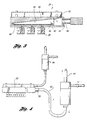
- a wave soldering apparatus 10 for soldering components to a circuit board 15.
- the apparatus includes a conveyor 12 situated in a tunnel 14 for transporting the board 15 through a pre-heat zone 16.
- the pre-heat zone 16 includes one or more heaters 32 located below the conveyor 12.
- Each distributing manifold 24 is mounted in the tunnel 14 above the conveyor 12 in the pre-heat zone 16.
- each distributing manifold 24 is mounted within 1.27 - 15.24 cm (0.5 - 6.0 inches) of the circuit board's surface.
- the waves include a turbulent wave 18 and a laminar flow wave 20. Thereafter, the board passes through a cool down zone 22.
- the board Before passing through the turbulent wave 18, the board passes through a spray flux unit 38 and heaters 32 which deliver thermal energy to an underside of the circuit board 15 before it engages the turbulent and laminar flow waves 18,20 of the solder pot.
- At least one distributing manifold or plenum 24 is mounted in the tunnel 14.
- Each manifold 24 has an inlet port 26 ( Figure 3) for receiving a cold gas under pressure.
- the cold gas emerges from the distributing manifold 24 through at least one outlet nozzle 28 for directing the cold gas to the circuit board, thereby rapidly cooling the circuit board and the components. In this manner, the cold effluent from each outlet nozzle 28 functions as a cold gas knife.
- one or more distributing manifolds 66 are mounted in the tunnel 14 in the cool down zone. Those manifolds 66 may be mounted either above or below, or both above and below, the conveyor 12 and the circuit board. Optionally, the manifold 66 may cool the bottom side of the circuit board 15 after solder reflow.
- Figure 1 depicts a configuration of the wave soldering apparatus wherein the least one distributing manifold 66 is mounted in the tunnel 14 adjacent the exit from the laminar flow wave 20 of the solder wave. Care is needed in locating the at least one distributing manifold 66 so that it does not freeze or chill the solder waves. In practice, about 12 inches of separation between the laminar wave and the manifold 66 is sufficient. Thus, the distributing manifold(s) situated in the cool down zone effectively cool solder joints quickly, thereby promoting a small grain size and consequent improvement in fatigue properties. Typical cooling rates amount to about 2° - 10°C per second.
- the cold gas is furnished by a vortex cooling device 30.
- the vortex device of Figure 2 conventionally includes a vortex tube having an inlet 40 which receives compressed air, typically at about 21°C (70°F) through the vortex tube inlet 40.
- Incoming air is delivered to a vortex-generation chamber from which cold air emerges through a cooled stream 42, typically at about -46°C (-50°F).
- Warm air exhausts from the vortex warm outlet 44, typically at about 93°C (200°F).
- a suitable vortex tube is available from ITW Vortec, Cincinnati, Ohio.
- Other suitable devices are available from EXAIR Corporation, also Cincinnati, Ohio. Such designs operate on the vortex principle of fluid rotating about an axis.
- the vortex tube creates a vortex from compressed air and separates it into two streams - one hot and one cold.
- compressed air or an inert gas enters a cylindrical generator that is proportionally larger than the hot (long) tube, where it causes the air to rotate. Rotating air is forced down the inner walls of hot tube at speeds reaching 1,000,000 rpm.
- the hot tube At the end of the hot tube, a small portion of this air exits through a needle valve as hot air exhaust. The remaining air is forced back to the centre of the incoming air stream at a slower speed. The heat from the slower moving air is transferred to the faster moving incoming air.
- the super-cooled air flows through the centre of the generator and exits through the cold air exhaust port 42. The result is that air up to 121°C (250°F) emerges from one end of the tube and air at about -46°C (-50°F) emerges from the other end.
- the tube operates on filtered factory compressed air at about 1.51 Pa (100psig) and 21°C (70°F).
- gas is supplied to the vortex cooling device 30 at a pressure of approximately 0.15-1.82 Pa (10-120 psig).
- Such vortex cooling devices represent means for converting a supply of gas entering the device through a vortex tube inlet 40. Such gas is converted into a cooled stream which is delivered to the inlet port 26 ( Figure 3) of the distributing manifold 24 and a heated stream delivered from the vortex warm exhaust outlet port 44 ( Figure 2) to augment an inert gas flow 36 within the tunnel, thereby minimising oxidation of the solder.
- inert gases include nitrogen, argon, and carbon dioxide.
- the warm stream replenishes inert gas entering the system, thereby effectively using heat and the inert gas.
- the invention has utility in heating large thermally-dense components on the circuit board, or the circuit board itself. In some configurations in which large parts or large components are involved, temperature rise does not occur as quickly as with smaller parts. Accordingly, the invention has the attribute of augmenting heat supply to a top side of a circuit board if desired.
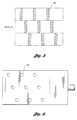
- the cooled gas emerges from the at least one outlet nozzle 28 to define a spray pattern which is directed toward the circuit board.
- the nozzle configuration can be selected so as to control or direct the spray pattern 46 ( Figure 5) to specific areas, or to an entire surface of the circuit board 15.
- the at least one outlet nozzle 28 comprises three rows of outlet nozzles. Each row has three nozzles. Each nozzle projects a shaped volume of gas upon a surface of the circuit board. Depending on the nozzle selected, the shaped volume may be generally elliptical, as shown, or rectangular, if desired. In this way, the volume of gas projected from each nozzle projects an array of shaped distribution patterns ( Figure 5) which impinge upon the circuit board.
- each distributing manifold 24 may be provided with hollow walls 50 which define a space through which coolant may pass to maintain refrigeration or thermal insulation of gas passing through a central chamber 52 of the distributing manifold 24.
- a vacuum can be drawn to act as a thermal barrier to protect the central chamber 52 from being heated by high tunnel temperatures.
- the wave soldering apparatus 10 may include a second vortex cooling device 64 which is connected to the hollow wall 50 of the distributing manifold 24 for supplying cool air to a jacketing chamber about the plenum to prevent external heat from affecting the cold spray within the plenum.
- a second vortex cooling device 64 which is connected to the hollow wall 50 of the distributing manifold 24 for supplying cool air to a jacketing chamber about the plenum to prevent external heat from affecting the cold spray within the plenum.
- each of the at least one distributing manifolds 24 has a central chamber 52 defined by walls 50, a floor to which the at least one outlet nozzle 28 is secured, and a sloping roof 58.
- the sloping roof 58 is inclined downwardly in relation to a wall 54 which is provided with the inlet port 26 to promote uniformity of pressure distribution throughout the chamber 52 of gas prior to emergence from the at least one outlet nozzle 28.
- gas distribution screens may be provided within the manifold. As illustrated in Figure 3, a gas distribution screen 60 is provided generally parallel to the floor 56. Alternatively, or in addition, a gas distribution screen is provided at an angle to the floor, such as orthogonal thereto.
- At least one outlet nozzle 28 directs the cold gas to the heated surface of the circuit board in a direction which is inclined thereto at an acute angle and against the direction of movement of the board 15 along the conveyor 12 in the tunnel 14.
- the disclosed apparatus includes process steps comprising:
Landscapes
- Engineering & Computer Science (AREA)
- Mechanical Engineering (AREA)
- Electric Connection Of Electric Components To Printed Circuits (AREA)
- Molten Solder (AREA)
- Cooling Or The Like Of Electrical Apparatus (AREA)
- Lining Or Joining Of Plastics Or The Like (AREA)
Claims (7)
- Vorrichtung zum Löten von Komponenten auf einer Leiterplatte (15), welche Vorrichtung ein Förderband (12) in einem Tunnel (14) aufweist, zur Weiterförderung der Leiterplatte (15) durch eine Vorwärmzone (16), Schmelzbadwellen flüssigen Lotes, mit einer turbulenten Welle (18) und einer laminaren Welle (20), eine Abkühlzone (22), durch welche die Leiterplatte läuft, wenn sie aus der Laminarströmungswelle der Lötwellen austritt, wenigstens einen Verteiler (24, 66), welcher in dem Tunnel angebracht ist und eine Einlaßöffnung (26) zum Empfang von kaltem, unter Druck stehendem Gas aufweist, und wenigstens eine Auslaßdüse (28), die das kalte Gas auf die Leiterplatte (15) richtet, so daß die Leiterplatte (15) und die Komponenten rasch abgekühlt werden, und eine Wirbelrohr-Kühlvorrichtung (30), die an der Einlaßöffnung des Verteilers angeschlossen ist, zur Abgabe des unter Druck stehenden kalten Gases,
dadurch gekennzeichnet, daß die Wirbelrohr-Kühlvorrichtung (30) Mittel beinhaltet, welche eine Zufuhr von durch einen Wirbelrohr-Einlaß (40) in die Vorrichtung (30) eintretendem Gas in einen kalten Gasstrom umwandelt, der der Einlaßöffnung (26) des Verteilers zugeführt wird, und in einen warmen Strom zur Erhöhung des Inertgasstromes im Tunnel (14) zur Minimierung der Oxydation des Lotes. - Vorrichtung nach Anspruch 1, worin die Vorwärmzone (16) ein oder mehrere unter dem Förderband (12) angeordnete Heizelemente (32) aufweist, und der Verteiler oder Sammler oder jeder der Verteiler (24) im Tunnel (14) über dem Förderband (12) in der Vorwärmzone (16) montiert ist.
- Vorrichtung nach Anspruch 1 oder 2, mit wenigstens zwei in der Vorwärmzone (16) angebrachten Verteilern (24).
- Vorrichtung nach einem beliebigen der vorangehenden Ansprüche, mit wenigstens einem im Tunnel (16) in der Abkühlzone (22) angebrachten Verteiler (66).
- Vorrichtung nach einem beliebigen der vorangehenden Ansprüche, worin der Verteiler bzw. jeder der Verteiler (24) drei Reihen von Düsen (28) aufweist, wobei jede Reihe drei Düsen (28) aufweist, wobei jede Düse (28) ein geformtes Gasvolumen aussprüht, das auf die Leiterplatte (15) auftrifft, so daß das aus der Düse ausgesprühte Gasvolumen ein Raster von geformten Verteilungsmustern bildet.
- Vorrichtung nach einem beliebigen der Ansprüche 1 bis 4, worin der Verteiler oder jeder der Verteiler (24) mit Hohlwänden (50) versehen ist, welche einen Raum bilden, durch welchen ein Kühlmittel fließen kann, um die Kühlung des durch die zentrale Kammer (52) des Verteilers (24) strömenden Gases aufrecht zu erhalten.
- Vorrichtung nach einem beliebigen der Ansprüche 1 bis 4, worin der Verteiler oder jeder der Verteiler (24) eine zentrale Kammer (52) aufweist, die durch Wände (50), einen Boden, an welchem die besagte wenigstens eine Auslaßdüse befestigt ist, und ein geneigtes Dach (58) begrenzt wird, wobei das Dach (58) in bezug auf eine mit der Einlaßöffnung (26) versehene Wand (54) abwärts geneigt ist, um die Gleichmäßigkeit der Druckverteilung des Gases in der Kammer (52) zu fördern, bevor das Gas aus der besagten wenigstens einen Auslaßdüse (28) austritt.
Applications Claiming Priority (2)
| Application Number | Priority Date | Filing Date | Title |
|---|---|---|---|
| US524662 | 1995-09-08 | ||
| US08/524,662 US5685475A (en) | 1995-09-08 | 1995-09-08 | Apparatus for cooling printed circuit boards in wave soldering |
Publications (2)
| Publication Number | Publication Date |
|---|---|
| EP0761361A1 EP0761361A1 (de) | 1997-03-12 |
| EP0761361B1 true EP0761361B1 (de) | 2001-11-14 |
Family
ID=24090165
Family Applications (1)
| Application Number | Title | Priority Date | Filing Date |
|---|---|---|---|
| EP96306340A Expired - Lifetime EP0761361B1 (de) | 1995-09-08 | 1996-09-02 | Gerät zum Abkühlen von gedruckten Schaltungsplatten beim Wellenlöten |
Country Status (5)
| Country | Link |
|---|---|
| US (1) | US5685475A (de) |
| EP (1) | EP0761361B1 (de) |
| JP (1) | JPH0983125A (de) |
| DE (1) | DE69616912T2 (de) |
| ES (1) | ES2169212T3 (de) |
Families Citing this family (16)
| Publication number | Priority date | Publication date | Assignee | Title |
|---|---|---|---|---|
| DE4416788C2 (de) * | 1994-05-06 | 1999-08-19 | Siemens Ag | Verfahren zum Wellenlöten von Leiterplatten |
| DE19632335C2 (de) * | 1996-08-10 | 1999-01-21 | Messer Griesheim Gmbh | Verfahren und Vorrichtung zur mechanischen Beseitigung von Lotkugeln auf der Obfläche von Leiterplatten |
| JP3638415B2 (ja) * | 1997-01-20 | 2005-04-13 | 日本電熱計器株式会社 | ガス雰囲気はんだ付け装置 |
| US5993500A (en) * | 1997-10-16 | 1999-11-30 | Speedline Technololies, Inc. | Flux management system |
| JP2000244108A (ja) * | 1999-02-22 | 2000-09-08 | Senju Metal Ind Co Ltd | プリント基板のはんだ付け方法、プリント基板のはんだ付け装置およびはんだ付け装置用冷却装置 |
| TW516346B (en) * | 1999-04-06 | 2003-01-01 | Eighttech Tectron Co Ltd | Device for heating printed-circuit board |
| JP4332281B2 (ja) * | 2000-04-26 | 2009-09-16 | 株式会社日立製作所 | 電子装置の製造方法およびはんだ付け装置 |
| US6648216B2 (en) * | 2000-08-21 | 2003-11-18 | Matsushita Electric Industrial Co., Ltd. | Process and apparatus for flow soldering |
| WO2002028156A1 (en) * | 2000-09-26 | 2002-04-04 | Matsushita Electric Industrial Co., Ltd. | Method and device for flow soldering |
| US6401463B1 (en) | 2000-11-29 | 2002-06-11 | Marconi Communications, Inc. | Cooling and heating system for an equipment enclosure using a vortex tube |
| US7565808B2 (en) * | 2005-01-13 | 2009-07-28 | Greencentaire, Llc | Refrigerator |
| DE502007006711D1 (de) | 2006-05-23 | 2011-04-28 | Linde Ag | Vorrichtung und Verfahren zum Wellenlöten |
| US7726135B2 (en) * | 2007-06-06 | 2010-06-01 | Greencentaire, Llc | Energy transfer apparatus and methods |
| US9198300B2 (en) * | 2014-01-23 | 2015-11-24 | Illinois Tool Works Inc. | Flux management system and method for a wave solder machine |
| DE102015106298B4 (de) * | 2015-04-24 | 2017-01-26 | Semikron Elektronik Gmbh & Co. Kg | Vorrichtung, Verfahren und Anlage zur inhomogenen Abkühlung eines flächigen Gegenstandes |
| WO2023243575A1 (ja) * | 2022-06-13 | 2023-12-21 | 千住金属工業株式会社 | 噴流はんだ付け装置 |
Family Cites Families (15)
| Publication number | Priority date | Publication date | Assignee | Title |
|---|---|---|---|---|
| US3579853A (en) * | 1968-12-05 | 1971-05-25 | Joseph J Martino | Circuit board drier |
| US3724418A (en) * | 1971-08-20 | 1973-04-03 | Lain J Mc | Solder coating apparatus |
| DE2932398C2 (de) * | 1979-08-09 | 1981-10-15 | Siemens AG, 1000 Berlin und 8000 München | Vorrichtung zum Kühlen von Leiterplatten nach dem maschinellen Einlöten von elektrischen Bauteilen |
| US4390120A (en) * | 1980-12-15 | 1983-06-28 | Bell Telephone Laboratories, Incorporated | Soldering methods and apparatus |
| EP0058766B1 (de) * | 1981-02-23 | 1985-08-07 | Matsushita Electric Industrial Co., Ltd. | Lötapparat |
| JPS6281264A (ja) * | 1985-10-02 | 1987-04-14 | Alps Electric Co Ltd | 半田付装置 |
| DE3611180C1 (en) * | 1986-04-03 | 1987-01-29 | Siemens Ag | Device for cooling soldered-work carrier and solder deposit in soldering units |
| US4679720A (en) * | 1986-10-23 | 1987-07-14 | Hollis Automation, Inc. | Mass soldering system providing a sweeping fluid blast |
| DE8700269U1 (de) * | 1987-01-07 | 1987-02-19 | ERSA Ernst Sachs KG, GmbH & Co, 6980 Wertheim | Wellenlötanlage |
| DE3737563A1 (de) * | 1987-11-05 | 1989-05-18 | Ernst Hohnerlein | Loetmaschine |
| DE3843191C2 (de) * | 1988-12-22 | 1994-09-15 | Broadcast Television Syst | Vorrichtung zum Löten |
| JPH0446666A (ja) * | 1990-05-31 | 1992-02-17 | Eiteitsuku Tekutoron Kk | リフロ―半田付け方法及び装置 |
| US5240169A (en) * | 1991-12-06 | 1993-08-31 | Electrovert Ltd. | Gas shrouded wave soldering with gas knife |
| JP2567336B2 (ja) * | 1993-04-23 | 1996-12-25 | 一郎 川勝 | 不活性雰囲気中のハンダ付け装置 |
| US5520320A (en) * | 1994-04-22 | 1996-05-28 | Air Liquide America Corporation | Process for wave soldering components on a printed circuit board in a temperature controlled non-oxidizing atmosphere |
-
1995
- 1995-09-08 US US08/524,662 patent/US5685475A/en not_active Expired - Fee Related
-
1996
- 1996-07-17 JP JP8187752A patent/JPH0983125A/ja active Pending
- 1996-09-02 DE DE69616912T patent/DE69616912T2/de not_active Expired - Fee Related
- 1996-09-02 EP EP96306340A patent/EP0761361B1/de not_active Expired - Lifetime
- 1996-09-02 ES ES96306340T patent/ES2169212T3/es not_active Expired - Lifetime
Also Published As
| Publication number | Publication date |
|---|---|
| EP0761361A1 (de) | 1997-03-12 |
| DE69616912T2 (de) | 2002-04-11 |
| ES2169212T3 (es) | 2002-07-01 |
| DE69616912D1 (de) | 2001-12-20 |
| JPH0983125A (ja) | 1997-03-28 |
| US5685475A (en) | 1997-11-11 |
Similar Documents
| Publication | Publication Date | Title |
|---|---|---|
| EP0761361B1 (de) | Gerät zum Abkühlen von gedruckten Schaltungsplatten beim Wellenlöten | |
| CA2161770C (en) | Process and apparatus for the wave soldering of circuit boards | |
| KR910005959B1 (ko) | 리플로우 납땜 방법 및 그 장치 | |
| CN215658308U (zh) | 一种波峰焊和回流焊均可以实现的焊接装置 | |
| EP1106294B1 (de) | Lötmaschine | |
| CA2224772C (en) | Gas knife cooling system | |
| US4361967A (en) | Device for cooling freshly-soldered circuit boards | |
| JP3877477B2 (ja) | リフローはんだ付け装置 | |
| US5878941A (en) | Method of soldering components on a carrier foil | |
| US20020047039A1 (en) | Automatic wave soldering apparatus and method | |
| JP2812675B2 (ja) | リフロー半田付け装置 | |
| JP2006153440A (ja) | 熱風噴射型加熱装置および加熱炉 | |
| US20040050915A1 (en) | System and method for mounting electronic components onto flexible substrates | |
| US6794616B1 (en) | Solder reflow oven | |
| JP3114278B2 (ja) | チッソリフロー装置 | |
| JP2004511089A (ja) | フレキシブル基板上に電子部品を取付けるためのシステム及び方法 | |
| JP2841885B2 (ja) | リフロー装置 | |
| JP2000059020A (ja) | 半田付け用片面リフロー炉の冷却装置 | |
| US6686565B2 (en) | Method of an apparatus for heating a substrate | |
| KR200396256Y1 (ko) | 리플로우 납땜장치 | |
| JPH0318469A (ja) | エアリフロー装置 | |
| JPH03198980A (ja) | 熱風リフロー装置 | |
| KR19980018549A (ko) | 인쇄회로기판의 표면상의 땜납 비드를 기계적으로 제거하는 방법 및 장치 | |
| JP2004237303A (ja) | リフロー式半田付装置における炉内熱気の流動方法及び流動装置 | |
| JP2913299B2 (ja) | リフロー半田付け装置 |
Legal Events
| Date | Code | Title | Description |
|---|---|---|---|
| PUAI | Public reference made under article 153(3) epc to a published international application that has entered the european phase |
Free format text: ORIGINAL CODE: 0009012 |
|
| AK | Designated contracting states |
Kind code of ref document: A1 Designated state(s): DE ES FR GB |
|
| 17P | Request for examination filed |
Effective date: 19970808 |
|
| 17Q | First examination report despatched |
Effective date: 19990427 |
|
| GRAG | Despatch of communication of intention to grant |
Free format text: ORIGINAL CODE: EPIDOS AGRA |
|
| GRAG | Despatch of communication of intention to grant |
Free format text: ORIGINAL CODE: EPIDOS AGRA |
|
| GRAH | Despatch of communication of intention to grant a patent |
Free format text: ORIGINAL CODE: EPIDOS IGRA |
|
| GRAH | Despatch of communication of intention to grant a patent |
Free format text: ORIGINAL CODE: EPIDOS IGRA |
|
| GRAA | (expected) grant |
Free format text: ORIGINAL CODE: 0009210 |
|
| AK | Designated contracting states |
Kind code of ref document: B1 Designated state(s): DE ES FR GB |
|
| REF | Corresponds to: |
Ref document number: 69616912 Country of ref document: DE Date of ref document: 20011220 |
|
| REG | Reference to a national code |
Ref country code: GB Ref legal event code: IF02 |
|
| REG | Reference to a national code |
Ref country code: ES Ref legal event code: FG2A Ref document number: 2169212 Country of ref document: ES Kind code of ref document: T3 |
|
| PGFP | Annual fee paid to national office [announced via postgrant information from national office to epo] |
Ref country code: FR Payment date: 20020909 Year of fee payment: 7 |
|
| PLBE | No opposition filed within time limit |
Free format text: ORIGINAL CODE: 0009261 |
|
| STAA | Information on the status of an ep patent application or granted ep patent |
Free format text: STATUS: NO OPPOSITION FILED WITHIN TIME LIMIT |
|
| PGFP | Annual fee paid to national office [announced via postgrant information from national office to epo] |
Ref country code: ES Payment date: 20020923 Year of fee payment: 7 |
|
| 26N | No opposition filed | ||
| PG25 | Lapsed in a contracting state [announced via postgrant information from national office to epo] |
Ref country code: ES Free format text: LAPSE BECAUSE OF NON-PAYMENT OF DUE FEES Effective date: 20030903 |
|
| PG25 | Lapsed in a contracting state [announced via postgrant information from national office to epo] |
Ref country code: FR Free format text: LAPSE BECAUSE OF NON-PAYMENT OF DUE FEES Effective date: 20040528 |
|
| REG | Reference to a national code |
Ref country code: FR Ref legal event code: ST |
|
| REG | Reference to a national code |
Ref country code: ES Ref legal event code: FD2A Effective date: 20030903 |
|
| PGFP | Annual fee paid to national office [announced via postgrant information from national office to epo] |
Ref country code: DE Payment date: 20070921 Year of fee payment: 12 |
|
| PGFP | Annual fee paid to national office [announced via postgrant information from national office to epo] |
Ref country code: GB Payment date: 20070914 Year of fee payment: 12 |
|
| GBPC | Gb: european patent ceased through non-payment of renewal fee |
Effective date: 20080902 |
|
| PG25 | Lapsed in a contracting state [announced via postgrant information from national office to epo] |
Ref country code: DE Free format text: LAPSE BECAUSE OF NON-PAYMENT OF DUE FEES Effective date: 20090401 |
|
| PG25 | Lapsed in a contracting state [announced via postgrant information from national office to epo] |
Ref country code: GB Free format text: LAPSE BECAUSE OF NON-PAYMENT OF DUE FEES Effective date: 20080902 |