EP0752784A2 - Bilderzeugungsgerät - Google Patents
Bilderzeugungsgerät Download PDFInfo
- Publication number
- EP0752784A2 EP0752784A2 EP96110908A EP96110908A EP0752784A2 EP 0752784 A2 EP0752784 A2 EP 0752784A2 EP 96110908 A EP96110908 A EP 96110908A EP 96110908 A EP96110908 A EP 96110908A EP 0752784 A2 EP0752784 A2 EP 0752784A2
- Authority
- EP
- European Patent Office
- Prior art keywords
- image
- line
- data
- image processing
- lines
- Prior art date
- Legal status (The legal status is an assumption and is not a legal conclusion. Google has not performed a legal analysis and makes no representation as to the accuracy of the status listed.)
- Granted
Links
Images






Classifications
-
- H—ELECTRICITY
- H04—ELECTRIC COMMUNICATION TECHNIQUE
- H04N—PICTORIAL COMMUNICATION, e.g. TELEVISION
- H04N25/00—Circuitry of solid-state image sensors [SSIS]; Control thereof
-
- H—ELECTRICITY
- H04—ELECTRIC COMMUNICATION TECHNIQUE
- H04N—PICTORIAL COMMUNICATION, e.g. TELEVISION
- H04N25/00—Circuitry of solid-state image sensors [SSIS]; Control thereof
- H04N25/70—SSIS architectures; Circuits associated therewith
- H04N25/701—Line sensors
Definitions
- reading speed can be determined by the operation frequency of the CCD and the number of photo-diodes. In order to increase reading speed, it is necessary to further increase operation frequency. However, since there is a limit to operation frequency, in order to further increase the speed, it is necessary to sacrifice resolution. So far, it was difficult to be compatible high resolution and high speed reading.
- the first embodiment for attaining the above-mentioned second object is an image reading apparatus which obtains two-dimensional original image information due to the above-mentioned one-dimensional image sensor by moving aforesaid image sensor and the original relatively in the secondary scanning direction while the original is scanned in the primary scanning direction by a one-dimensional image sensor, wherein the element rows of two or more one-dimensional image sensor is positioned parallelly, image reading by means of each one-dimensional image sensor is concurrently conducted and one-dimensional image sensors read images located in different lines from each other in the secondary scanning direction.
- the structure of the sixth embodiment is that the scanning speed in the above-mentioned secondary scanning direction is n times the speed at which a prescribed resolution can be obtained with one one-dimensional image sensor and outputting corresponding with each line at a prescribed resolution is calculated based on outputting from each of the above-mentioned one-dimensional image sensors.
- first line of adjacent lines is defined to be an "odd line”, and any adjacent line is defined to be an "even line”.
- the first line, third line, ..., (L-1)th line are called odd lines, and the 2nd line, 4th line, ..., Lth line are called even lines.
- Fig. 3 is a time chart showing operation timing of the image separation circuit.
- Fig. 6 is a block diagram showing a practical example of a frequency conversion circuit.
- Fig. 7 is a timing chart showing operation of the frequency conversion circuit shown in Fig. 6.
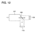
- CCD line sensors 109 and 110 equipped with a shutter function and thereby to control charge accumulation time due to the above-mentioned shutter function so that images without image blur in the secondary scanning direction are obtained.
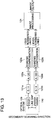
- charge accumulation time is controlled in such a manner as to be less than the frequency (one-line outputting frequency) of control signal SH by means of the above-mentioned signals SHUT 1 and 2, time wherein charge is actually accumulated during aforesaid accumulation time is controlled and thereby accumulation of optical signal for 2 lines can be avoided, though conveyance in a secondary scanning direction for 2 lines in conversion to 400 dpi is being conducted. Therefore, due to synthesizing outputting from each CCD line sensors 109 and 110 as data for odd lines and even lines, a blurless image in the secondary scanning direction can be obtained.
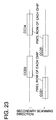
- each CCD line sensor 109 and 110 in the secondary scanning direction is 267 dpi.
- Each CCD line sensor 109 and 110 reads 1.5 lines when converting to 400 dpi.
- light signal accumulation time which is frequency of control signals SH1 and 2
- an optical signal for 1.5 lines is accumulated.
- each of adjoining lines are read at a prescribed resolution. Accordingly, reading speed can be increased.
Landscapes
- Engineering & Computer Science (AREA)
- Multimedia (AREA)
- Signal Processing (AREA)
- Facsimile Scanning Arrangements (AREA)
- Facsimile Image Signal Circuits (AREA)
- Editing Of Facsimile Originals (AREA)
- Storing Facsimile Image Data (AREA)
Applications Claiming Priority (6)
| Application Number | Priority Date | Filing Date | Title |
|---|---|---|---|
| JP17087895 | 1995-07-06 | ||
| JP17087895A JP3458203B2 (ja) | 1995-07-06 | 1995-07-06 | 画像処理装置 |
| JP170878/95 | 1995-07-06 | ||
| JP19059795 | 1995-07-26 | ||
| JP190597/95 | 1995-07-26 | ||
| JP7190597A JPH0946477A (ja) | 1995-07-26 | 1995-07-26 | 画像読取り装置 |
Publications (3)
| Publication Number | Publication Date |
|---|---|
| EP0752784A2 true EP0752784A2 (de) | 1997-01-08 |
| EP0752784A3 EP0752784A3 (de) | 1998-04-15 |
| EP0752784B1 EP0752784B1 (de) | 2002-03-06 |
Family
ID=26493759
Family Applications (1)
| Application Number | Title | Priority Date | Filing Date |
|---|---|---|---|
| EP96110908A Expired - Lifetime EP0752784B1 (de) | 1995-07-06 | 1996-07-05 | Bilderzeugungsgerät |
Country Status (3)
| Country | Link |
|---|---|
| US (1) | US5963344A (de) |
| EP (1) | EP0752784B1 (de) |
| DE (1) | DE69619601T2 (de) |
Cited By (2)
| Publication number | Priority date | Publication date | Assignee | Title |
|---|---|---|---|---|
| EP0969660A3 (de) * | 1998-07-03 | 2000-11-08 | Canon Kabushiki Kaisha | Taktsteuerungsvorrichtung zur Bilderzeugung |
| EP1168814A3 (de) * | 2000-06-27 | 2004-05-19 | Canon Kabushiki Kaisha | Bildverarbeitungsvorrichtung und Verarbeitungsverfahren dafür |
Families Citing this family (15)
| Publication number | Priority date | Publication date | Assignee | Title |
|---|---|---|---|---|
| JPH10173859A (ja) * | 1996-12-09 | 1998-06-26 | Canon Inc | アナログ信号処理回路 |
| JP3453506B2 (ja) * | 1998-01-27 | 2003-10-06 | 富士写真フイルム株式会社 | 画像読取装置 |
| US7315388B2 (en) * | 2001-01-24 | 2008-01-01 | Canon Kabushiki Kaisha | Image input/output control apparatus, image processing apparatus, image processing method, data communication apparatus, and data communication method |
| CN1254079C (zh) * | 2002-01-09 | 2006-04-26 | 索尼公司 | 图像读取设备和方法 |
| JP4278434B2 (ja) * | 2003-05-19 | 2009-06-17 | パナソニック株式会社 | 通信装置、情報共有システムおよび情報共有方法 |
| TWI245538B (en) * | 2004-07-28 | 2005-12-11 | Lite On Technology Corp | A high-speed image scanning system and method thereof |
| US7369151B2 (en) * | 2005-02-24 | 2008-05-06 | Kabushiki Kaisha Toshiba | Laser control circuit and image forming apparatus |
| JP4597932B2 (ja) * | 2006-09-19 | 2010-12-15 | 株式会社リコー | 画像読取信号処理icおよび画像読取装置と画像形成装置 |
| JP5448786B2 (ja) * | 2009-04-06 | 2014-03-19 | キヤノン株式会社 | 画像読取装置及びその制御方法 |
| JP5531690B2 (ja) * | 2010-03-16 | 2014-06-25 | 株式会社リコー | 画像読取装置及び画像形成装置 |
| JP6011247B2 (ja) * | 2012-10-29 | 2016-10-19 | ブラザー工業株式会社 | 画像処理システム,画像処理装置,および情報処理装置 |
| JP6197412B2 (ja) * | 2013-07-01 | 2017-09-20 | 株式会社リコー | 撮像装置、画像読取装置、画像形成装置、および撮像装置の駆動方法 |
| RU2623806C1 (ru) * | 2016-06-07 | 2017-06-29 | Акционерное общество Научно-производственный центр "Электронные вычислительно-информационные системы" (АО НПЦ "ЭЛВИС") | Способ и устройство обработки стереоизображений |
| JP2018195985A (ja) * | 2017-05-17 | 2018-12-06 | キヤノン株式会社 | 画像処理装置、撮像装置、画像処理方法、プログラム、および、記憶媒体 |
| WO2022027155A1 (en) * | 2020-08-01 | 2022-02-10 | Huawei Technologies Co., Ltd. | Device and method for fingerprint sensing |
Family Cites Families (10)
| Publication number | Priority date | Publication date | Assignee | Title |
|---|---|---|---|---|
| US4474422A (en) * | 1979-11-13 | 1984-10-02 | Canon Kabushiki Kaisha | Optical scanning apparatus having an array of light sources |
| US4366509A (en) * | 1981-04-01 | 1982-12-28 | Minnesota Mining And Manufacturing Co. | Facsimile apparatus with multiple scanning and printing elements |
| JPS6411467A (en) * | 1987-07-03 | 1989-01-17 | Minolta Camera Kk | Image input device |
| US5315412A (en) * | 1990-04-06 | 1994-05-24 | Canon Kabushiki Kaisha | Multi-chip color image sensor with light-receiving windows arranged to provide sensor output signals corresponding to the gap between adjacent sensors |
| JP3086696B2 (ja) * | 1990-08-24 | 2000-09-11 | 株式会社東芝 | 画像信号処理装置 |
| JP2856940B2 (ja) * | 1991-05-15 | 1999-02-10 | 株式会社東芝 | 画像読取り装置 |
| JPH05328039A (ja) * | 1992-05-25 | 1993-12-10 | Ricoh Co Ltd | 画像読取装置 |
| JPH07111561A (ja) * | 1993-10-12 | 1995-04-25 | Matsushita Electric Ind Co Ltd | 原稿読み取り装置 |
| US5483053A (en) * | 1994-09-27 | 1996-01-09 | Hewlett-Packard Company | Variable resolution color image scanner having an exposure delay between successive linear photosensors detecting different colors |
| US5550653A (en) * | 1995-06-05 | 1996-08-27 | Xerox Corporation | Color sensor array and system for scanning simple color documents |
-
1996
- 1996-06-28 US US08/671,710 patent/US5963344A/en not_active Expired - Lifetime
- 1996-07-05 EP EP96110908A patent/EP0752784B1/de not_active Expired - Lifetime
- 1996-07-05 DE DE69619601T patent/DE69619601T2/de not_active Expired - Lifetime
Cited By (3)
| Publication number | Priority date | Publication date | Assignee | Title |
|---|---|---|---|---|
| EP0969660A3 (de) * | 1998-07-03 | 2000-11-08 | Canon Kabushiki Kaisha | Taktsteuerungsvorrichtung zur Bilderzeugung |
| US6493830B2 (en) | 1998-07-03 | 2002-12-10 | Canon Kabushiki Kaisha | Clock control device used in image formation |
| EP1168814A3 (de) * | 2000-06-27 | 2004-05-19 | Canon Kabushiki Kaisha | Bildverarbeitungsvorrichtung und Verarbeitungsverfahren dafür |
Also Published As
| Publication number | Publication date |
|---|---|
| DE69619601T2 (de) | 2002-11-07 |
| US5963344A (en) | 1999-10-05 |
| DE69619601D1 (de) | 2002-04-11 |
| EP0752784A3 (de) | 1998-04-15 |
| EP0752784B1 (de) | 2002-03-06 |
Similar Documents
| Publication | Publication Date | Title |
|---|---|---|
| US5963344A (en) | Image forming apparatus | |
| JP6205885B2 (ja) | 光電変換素子、画像読取装置、画像形成装置及び画像読取方法 | |
| US4438457A (en) | High resolution imager employing staggered sensor structure | |
| EP0431159B1 (de) | Verfahren und anordnung zur erzeugung eines hochauflösenden elektronischen signals von der zeilenabtastung einer farbvorlage | |
| US4432017A (en) | Adjacent bilinear photosite imager | |
| JP2907058B2 (ja) | 蓄積手段を持つイメージセンサ及び画像読取装置 | |
| US6118481A (en) | Solid state image pick-up device and image pick-up apparatus | |
| EP1168814B1 (de) | Bildverarbeitungsvorrichtung und Verarbeitungsverfahren dafür | |
| JP2018011328A (ja) | 光電変換素子、画像読取装置、画像形成装置及び画像読取方法 | |
| US8542420B2 (en) | Image reading apparatus, image forming apparatus and method | |
| US5262631A (en) | Color image reading apparatus | |
| JPH10173868A (ja) | 固体撮像素子およびこれを備えた画像読取装置 | |
| US6567189B1 (en) | Image reading apparatus | |
| JPH0946477A (ja) | 画像読取り装置 | |
| US20020030861A1 (en) | Image scanning apparatus | |
| JPH07322151A (ja) | 固体撮像装置 | |
| JP3337055B2 (ja) | 画像読取装置 | |
| GB2370712A (en) | Photosensor array with decreased scan time for decreased resolution | |
| EP1148710A2 (de) | Farbbildaufnahmeelement, Bildleser mit diesem Bildaufnahmeelement, und Bildleseverfahren | |
| JP2563000B2 (ja) | 高速度カラービデオカメラ | |
| JP3829772B2 (ja) | 画像読取装置 | |
| JP2576987B2 (ja) | カラ−画像読取り装置 | |
| JPS6120467A (ja) | 画像形成装置 | |
| JPH0548841A (ja) | Ccdラインセンサ | |
| JPH0923317A (ja) | 画像処理装置 |
Legal Events
| Date | Code | Title | Description |
|---|---|---|---|
| PUAI | Public reference made under article 153(3) epc to a published international application that has entered the european phase |
Free format text: ORIGINAL CODE: 0009012 |
|
| AK | Designated contracting states |
Kind code of ref document: A2 Designated state(s): DE GB |
|
| PUAL | Search report despatched |
Free format text: ORIGINAL CODE: 0009013 |
|
| AK | Designated contracting states |
Kind code of ref document: A3 Designated state(s): DE FR GB IT NL |
|
| 17P | Request for examination filed |
Effective date: 19981006 |
|
| 17Q | First examination report despatched |
Effective date: 20000112 |
|
| GRAG | Despatch of communication of intention to grant |
Free format text: ORIGINAL CODE: EPIDOS AGRA |
|
| GRAG | Despatch of communication of intention to grant |
Free format text: ORIGINAL CODE: EPIDOS AGRA |
|
| GRAH | Despatch of communication of intention to grant a patent |
Free format text: ORIGINAL CODE: EPIDOS IGRA |
|
| GRAH | Despatch of communication of intention to grant a patent |
Free format text: ORIGINAL CODE: EPIDOS IGRA |
|
| REG | Reference to a national code |
Ref country code: GB Ref legal event code: IF02 |
|
| GRAA | (expected) grant |
Free format text: ORIGINAL CODE: 0009210 |
|
| RBV | Designated contracting states (corrected) |
Designated state(s): DE GB |
|
| AK | Designated contracting states |
Kind code of ref document: B1 Designated state(s): DE GB |
|
| REF | Corresponds to: |
Ref document number: 69619601 Country of ref document: DE Date of ref document: 20020411 |
|
| PLBE | No opposition filed within time limit |
Free format text: ORIGINAL CODE: 0009261 |
|
| STAA | Information on the status of an ep patent application or granted ep patent |
Free format text: STATUS: NO OPPOSITION FILED WITHIN TIME LIMIT |
|
| 26N | No opposition filed |
Effective date: 20021209 |
|
| PGFP | Annual fee paid to national office [announced via postgrant information from national office to epo] |
Ref country code: GB Payment date: 20110629 Year of fee payment: 16 |
|
| PGFP | Annual fee paid to national office [announced via postgrant information from national office to epo] |
Ref country code: DE Payment date: 20110629 Year of fee payment: 16 |
|
| GBPC | Gb: european patent ceased through non-payment of renewal fee |
Effective date: 20120705 |
|
| PG25 | Lapsed in a contracting state [announced via postgrant information from national office to epo] |
Ref country code: GB Free format text: LAPSE BECAUSE OF NON-PAYMENT OF DUE FEES Effective date: 20120705 Ref country code: DE Free format text: LAPSE BECAUSE OF NON-PAYMENT OF DUE FEES Effective date: 20130201 |
|
| REG | Reference to a national code |
Ref country code: DE Ref legal event code: R119 Ref document number: 69619601 Country of ref document: DE Effective date: 20130201 |