EP0749161B1 - Integriertes Dünnschicht-Sonnenzellenmodul und Herstellungsverfahren - Google Patents
Integriertes Dünnschicht-Sonnenzellenmodul und Herstellungsverfahren Download PDFInfo
- Publication number
- EP0749161B1 EP0749161B1 EP96109504A EP96109504A EP0749161B1 EP 0749161 B1 EP0749161 B1 EP 0749161B1 EP 96109504 A EP96109504 A EP 96109504A EP 96109504 A EP96109504 A EP 96109504A EP 0749161 B1 EP0749161 B1 EP 0749161B1
- Authority
- EP
- European Patent Office
- Prior art keywords
- layer
- electrically conductive
- layers
- electrode
- electrode layer
- Prior art date
- Legal status (The legal status is an assumption and is not a legal conclusion. Google has not performed a legal analysis and makes no representation as to the accuracy of the status listed.)
- Expired - Lifetime
Links
- 239000010409 thin film Substances 0.000 title claims description 60
- 238000004519 manufacturing process Methods 0.000 title claims description 14
- 239000004065 semiconductor Substances 0.000 claims description 69
- 238000000034 method Methods 0.000 claims description 59
- XLOMVQKBTHCTTD-UHFFFAOYSA-N Zinc monoxide Chemical compound [Zn]=O XLOMVQKBTHCTTD-UHFFFAOYSA-N 0.000 claims description 43
- 239000000758 substrate Substances 0.000 claims description 31
- 239000011787 zinc oxide Substances 0.000 claims description 21
- 239000000463 material Substances 0.000 claims description 17
- XOLBLPGZBRYERU-UHFFFAOYSA-N tin dioxide Chemical compound O=[Sn]=O XOLBLPGZBRYERU-UHFFFAOYSA-N 0.000 claims description 17
- 229910044991 metal oxide Inorganic materials 0.000 claims description 13
- 150000004706 metal oxides Chemical class 0.000 claims description 13
- 229910052751 metal Inorganic materials 0.000 claims description 10
- 239000002184 metal Substances 0.000 claims description 10
- 229910052709 silver Inorganic materials 0.000 claims description 10
- 238000000151 deposition Methods 0.000 claims description 7
- AMGQUBHHOARCQH-UHFFFAOYSA-N indium;oxotin Chemical compound [In].[Sn]=O AMGQUBHHOARCQH-UHFFFAOYSA-N 0.000 claims description 5
- 229910001887 tin oxide Inorganic materials 0.000 claims description 5
- XLYOFNOQVPJJNP-UHFFFAOYSA-N water Substances O XLYOFNOQVPJJNP-UHFFFAOYSA-N 0.000 claims description 5
- 239000004332 silver Substances 0.000 claims description 4
- 239000001257 hydrogen Substances 0.000 claims description 3
- 229910052739 hydrogen Inorganic materials 0.000 claims description 3
- UFHFLCQGNIYNRP-UHFFFAOYSA-N Hydrogen Chemical compound [H][H] UFHFLCQGNIYNRP-UHFFFAOYSA-N 0.000 claims 2
- 239000007769 metal material Substances 0.000 claims 2
- 238000002955 isolation Methods 0.000 claims 1
- 239000010410 layer Substances 0.000 description 256
- 238000004140 cleaning Methods 0.000 description 28
- 239000010408 film Substances 0.000 description 23
- 230000008569 process Effects 0.000 description 23
- 239000007789 gas Substances 0.000 description 16
- 238000010248 power generation Methods 0.000 description 13
- 229910021417 amorphous silicon Inorganic materials 0.000 description 12
- 238000006243 chemical reaction Methods 0.000 description 10
- BLRPTPMANUNPDV-UHFFFAOYSA-N Silane Chemical compound [SiH4] BLRPTPMANUNPDV-UHFFFAOYSA-N 0.000 description 9
- 238000000926 separation method Methods 0.000 description 9
- 239000000853 adhesive Substances 0.000 description 8
- 230000001070 adhesive effect Effects 0.000 description 8
- 230000006872 improvement Effects 0.000 description 8
- 229910052782 aluminium Inorganic materials 0.000 description 6
- 238000004544 sputter deposition Methods 0.000 description 6
- XUIMIQQOPSSXEZ-UHFFFAOYSA-N Silicon Chemical compound [Si] XUIMIQQOPSSXEZ-UHFFFAOYSA-N 0.000 description 5
- 229910052804 chromium Inorganic materials 0.000 description 5
- 230000008021 deposition Effects 0.000 description 5
- 238000002474 experimental method Methods 0.000 description 5
- TWNQGVIAIRXVLR-UHFFFAOYSA-N oxo(oxoalumanyloxy)alumane Chemical compound O=[Al]O[Al]=O TWNQGVIAIRXVLR-UHFFFAOYSA-N 0.000 description 5
- 229910052710 silicon Inorganic materials 0.000 description 5
- 239000010703 silicon Substances 0.000 description 5
- XKRFYHLGVUSROY-UHFFFAOYSA-N Argon Chemical compound [Ar] XKRFYHLGVUSROY-UHFFFAOYSA-N 0.000 description 4
- 230000015572 biosynthetic process Effects 0.000 description 4
- 150000001875 compounds Chemical class 0.000 description 4
- 239000011521 glass Substances 0.000 description 4
- 239000013081 microcrystal Substances 0.000 description 4
- 238000012545 processing Methods 0.000 description 4
- 239000000047 product Substances 0.000 description 4
- 239000004020 conductor Substances 0.000 description 3
- 238000010586 diagram Methods 0.000 description 3
- 230000000694 effects Effects 0.000 description 3
- 230000010354 integration Effects 0.000 description 3
- VNWKTOKETHGBQD-UHFFFAOYSA-N methane Chemical compound C VNWKTOKETHGBQD-UHFFFAOYSA-N 0.000 description 3
- 238000000059 patterning Methods 0.000 description 3
- 238000005268 plasma chemical vapour deposition Methods 0.000 description 3
- 229910000077 silane Inorganic materials 0.000 description 3
- 238000005406 washing Methods 0.000 description 3
- 238000005275 alloying Methods 0.000 description 2
- 229910052786 argon Inorganic materials 0.000 description 2
- 230000015556 catabolic process Effects 0.000 description 2
- 238000007796 conventional method Methods 0.000 description 2
- 239000013078 crystal Substances 0.000 description 2
- 238000006731 degradation reaction Methods 0.000 description 2
- 239000003822 epoxy resin Substances 0.000 description 2
- 239000012467 final product Substances 0.000 description 2
- 238000012986 modification Methods 0.000 description 2
- 230000004048 modification Effects 0.000 description 2
- 238000002161 passivation Methods 0.000 description 2
- 229920000647 polyepoxide Polymers 0.000 description 2
- 238000007740 vapor deposition Methods 0.000 description 2
- VYZAMTAEIAYCRO-UHFFFAOYSA-N Chromium Chemical compound [Cr] VYZAMTAEIAYCRO-UHFFFAOYSA-N 0.000 description 1
- XYFCBTPGUUZFHI-UHFFFAOYSA-N Phosphine Chemical compound P XYFCBTPGUUZFHI-UHFFFAOYSA-N 0.000 description 1
- 229910000577 Silicon-germanium Inorganic materials 0.000 description 1
- BQCADISMDOOEFD-UHFFFAOYSA-N Silver Chemical compound [Ag] BQCADISMDOOEFD-UHFFFAOYSA-N 0.000 description 1
- LEVVHYCKPQWKOP-UHFFFAOYSA-N [Si].[Ge] Chemical compound [Si].[Ge] LEVVHYCKPQWKOP-UHFFFAOYSA-N 0.000 description 1
- 230000002411 adverse Effects 0.000 description 1
- XAGFODPZIPBFFR-UHFFFAOYSA-N aluminium Chemical compound [Al] XAGFODPZIPBFFR-UHFFFAOYSA-N 0.000 description 1
- 238000011161 development Methods 0.000 description 1
- ZOCHARZZJNPSEU-UHFFFAOYSA-N diboron Chemical compound B#B ZOCHARZZJNPSEU-UHFFFAOYSA-N 0.000 description 1
- 229910052732 germanium Inorganic materials 0.000 description 1
- GNPVGFCGXDBREM-UHFFFAOYSA-N germanium atom Chemical compound [Ge] GNPVGFCGXDBREM-UHFFFAOYSA-N 0.000 description 1
- 125000004435 hydrogen atom Chemical class [H]* 0.000 description 1
- 230000001788 irregular Effects 0.000 description 1
- 229910021421 monocrystalline silicon Inorganic materials 0.000 description 1
- 239000011241 protective layer Substances 0.000 description 1
- 238000001552 radio frequency sputter deposition Methods 0.000 description 1
- 239000002994 raw material Substances 0.000 description 1
- 238000012827 research and development Methods 0.000 description 1
- 239000000523 sample Substances 0.000 description 1
- 230000009291 secondary effect Effects 0.000 description 1
- HBMJWWWQQXIZIP-UHFFFAOYSA-N silicon carbide Chemical compound [Si+]#[C-] HBMJWWWQQXIZIP-UHFFFAOYSA-N 0.000 description 1
- 229910010271 silicon carbide Inorganic materials 0.000 description 1
- 239000002356 single layer Substances 0.000 description 1
- 238000009751 slip forming Methods 0.000 description 1
Images

Classifications
-
- H—ELECTRICITY
- H01—ELECTRIC ELEMENTS
- H01L—SEMICONDUCTOR DEVICES NOT COVERED BY CLASS H10
- H01L31/00—Semiconductor devices sensitive to infrared radiation, light, electromagnetic radiation of shorter wavelength or corpuscular radiation and specially adapted either for the conversion of the energy of such radiation into electrical energy or for the control of electrical energy by such radiation; Processes or apparatus specially adapted for the manufacture or treatment thereof or of parts thereof; Details thereof
- H01L31/02—Details
- H01L31/0224—Electrodes
- H01L31/022466—Electrodes made of transparent conductive layers, e.g. TCO, ITO layers
-
- H—ELECTRICITY
- H01—ELECTRIC ELEMENTS
- H01L—SEMICONDUCTOR DEVICES NOT COVERED BY CLASS H10
- H01L31/00—Semiconductor devices sensitive to infrared radiation, light, electromagnetic radiation of shorter wavelength or corpuscular radiation and specially adapted either for the conversion of the energy of such radiation into electrical energy or for the control of electrical energy by such radiation; Processes or apparatus specially adapted for the manufacture or treatment thereof or of parts thereof; Details thereof
- H01L31/02—Details
- H01L31/0224—Electrodes
- H01L31/022466—Electrodes made of transparent conductive layers, e.g. TCO, ITO layers
- H01L31/022475—Electrodes made of transparent conductive layers, e.g. TCO, ITO layers composed of indium tin oxide [ITO]
-
- H—ELECTRICITY
- H01—ELECTRIC ELEMENTS
- H01L—SEMICONDUCTOR DEVICES NOT COVERED BY CLASS H10
- H01L31/00—Semiconductor devices sensitive to infrared radiation, light, electromagnetic radiation of shorter wavelength or corpuscular radiation and specially adapted either for the conversion of the energy of such radiation into electrical energy or for the control of electrical energy by such radiation; Processes or apparatus specially adapted for the manufacture or treatment thereof or of parts thereof; Details thereof
- H01L31/02—Details
- H01L31/0224—Electrodes
- H01L31/022466—Electrodes made of transparent conductive layers, e.g. TCO, ITO layers
- H01L31/022483—Electrodes made of transparent conductive layers, e.g. TCO, ITO layers composed of zinc oxide [ZnO]
-
- H—ELECTRICITY
- H01—ELECTRIC ELEMENTS
- H01L—SEMICONDUCTOR DEVICES NOT COVERED BY CLASS H10
- H01L31/00—Semiconductor devices sensitive to infrared radiation, light, electromagnetic radiation of shorter wavelength or corpuscular radiation and specially adapted either for the conversion of the energy of such radiation into electrical energy or for the control of electrical energy by such radiation; Processes or apparatus specially adapted for the manufacture or treatment thereof or of parts thereof; Details thereof
- H01L31/04—Semiconductor devices sensitive to infrared radiation, light, electromagnetic radiation of shorter wavelength or corpuscular radiation and specially adapted either for the conversion of the energy of such radiation into electrical energy or for the control of electrical energy by such radiation; Processes or apparatus specially adapted for the manufacture or treatment thereof or of parts thereof; Details thereof adapted as photovoltaic [PV] conversion devices
- H01L31/042—PV modules or arrays of single PV cells
- H01L31/0445—PV modules or arrays of single PV cells including thin film solar cells, e.g. single thin film a-Si, CIS or CdTe solar cells
- H01L31/046—PV modules composed of a plurality of thin film solar cells deposited on the same substrate
-
- H—ELECTRICITY
- H01—ELECTRIC ELEMENTS
- H01L—SEMICONDUCTOR DEVICES NOT COVERED BY CLASS H10
- H01L31/00—Semiconductor devices sensitive to infrared radiation, light, electromagnetic radiation of shorter wavelength or corpuscular radiation and specially adapted either for the conversion of the energy of such radiation into electrical energy or for the control of electrical energy by such radiation; Processes or apparatus specially adapted for the manufacture or treatment thereof or of parts thereof; Details thereof
- H01L31/04—Semiconductor devices sensitive to infrared radiation, light, electromagnetic radiation of shorter wavelength or corpuscular radiation and specially adapted either for the conversion of the energy of such radiation into electrical energy or for the control of electrical energy by such radiation; Processes or apparatus specially adapted for the manufacture or treatment thereof or of parts thereof; Details thereof adapted as photovoltaic [PV] conversion devices
- H01L31/054—Optical elements directly associated or integrated with the PV cell, e.g. light-reflecting means or light-concentrating means
- H01L31/056—Optical elements directly associated or integrated with the PV cell, e.g. light-reflecting means or light-concentrating means the light-reflecting means being of the back surface reflector [BSR] type
-
- Y—GENERAL TAGGING OF NEW TECHNOLOGICAL DEVELOPMENTS; GENERAL TAGGING OF CROSS-SECTIONAL TECHNOLOGIES SPANNING OVER SEVERAL SECTIONS OF THE IPC; TECHNICAL SUBJECTS COVERED BY FORMER USPC CROSS-REFERENCE ART COLLECTIONS [XRACs] AND DIGESTS
- Y02—TECHNOLOGIES OR APPLICATIONS FOR MITIGATION OR ADAPTATION AGAINST CLIMATE CHANGE
- Y02E—REDUCTION OF GREENHOUSE GAS [GHG] EMISSIONS, RELATED TO ENERGY GENERATION, TRANSMISSION OR DISTRIBUTION
- Y02E10/00—Energy generation through renewable energy sources
- Y02E10/50—Photovoltaic [PV] energy
- Y02E10/52—PV systems with concentrators
Landscapes
- Engineering & Computer Science (AREA)
- Physics & Mathematics (AREA)
- Condensed Matter Physics & Semiconductors (AREA)
- Electromagnetism (AREA)
- General Physics & Mathematics (AREA)
- Computer Hardware Design (AREA)
- Microelectronics & Electronic Packaging (AREA)
- Power Engineering (AREA)
- Life Sciences & Earth Sciences (AREA)
- Sustainable Development (AREA)
- Sustainable Energy (AREA)
- Photovoltaic Devices (AREA)
Claims (16)
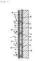
- Integrierte Dünnfilm-Solarbatterie (1), die mehrere in Reihe verbundene Elementeinheiten (15) hat, mit:dadurch gekennzeichnet, daßeinem Substrat (3);mehreren ersten Elektrodenschichten (5) aus transparentem leitendem Oxid, die in mehrere Bereiche aufgeteilt und auf dem Substrat (3) gebildet sind;mehreren Laminaten mit jeweils einer Halbleiterschicht (9) und einer auf die Halbleiterschicht (9) laminierten ersten elektrisch leitenden Schicht (11), die auf den ersten Elektrodenschichten (5) so angeordnet sind, daß jedes der Laminate auf zwei benachbarten ersten Elektroden (5) gebildet ist und eine Verbindungsöffnung (7) auf einer der beiden ersten Elektroden (5) hat, wobei die erste elektrisch leitende Schicht nicht in der Verbindungsöffnung gebildet ist; undzweiten Elektrodenschichten (13) aus metallischem Material, die auf jedem der Laminate in einem Zustand angeordnet sind, in dem die zweiten Elektrodenschichten (13) mit einer der beiden ersten Elektrodenschichten (5) durch die Verbindungsöffnung (7) elektrisch verbunden sind, um einen zwischen der zweiten Elektrodenschicht (13) und der anderen ersten Elektrodenschicht eingefügten Bereich als Elementeinheit (15) zu bilden;
die erste elektrisch leitende Schicht (11) aus einem transparenten Metalloxidmaterial besteht. - Integrierte Dünnfilm-Solarbatterie nach Anspruch 1, wobei die erste elektrisch leitende Schicht (11) eine Dicke in einem Bereich von 600 Å bis 1200 Å (10 Å = 1 nm) hat.
- Integrierte Dünnfilm-Solarbatterie nach Anspruch 1 oder 2, ferner mit einer zweiten elektrisch leitenden Schicht aus transparentem Metalloxid zwischen der ersten transparenten elektrisch leitenden Schicht (11) und der zweiten Elektrodenschicht (13).
- Integrierte Dünnfilm-Solarbatterie nach Anspruch 1, 2 oder 3, wobei die zweite Elektrodenschicht (13) aus Silber besteht.
- Integrierte Dünnfilm-Solarbatterie nach einem der Ansprüche 1 bis 4, wobei das transparente Metalloxidmaterial der ersten und zweiten transparenten elektrisch leitenden Schicht (11) aus Zinkoxid, Zinnoxid oder Indium-Zinn-Oxid besteht.
- Integrierte Dünnfilm-Solarbatterie nach einem der Ansprüche 1 bis 5, wobei die Halbleiterschichten (9) mit Wasserstoff dotiert sind.
- Integrierte Dünnfilm-Solarbatterie nach einem der Ansprüche 3 bis 6, wobei die Gesamtdicke der ersten und zweiten transparenten Metalloxidschicht auf 1000 Å eingestellt ist.
- Verfahren zur Herstellung einer integrierten Dünnfilm-Solarbatterie (1), die mehrere in Reihe verbundene Elementeinheiten (15) hat, mit den folgenden Schritten in der genannten Reihenfolge:dadurch gekennzeichnet, daßBilden mehrerer erster Elektrodenschichten (5) aus transparentem leitendem Oxid auf einem Substrat (3), wobei jede der Schichten (5) die erste Schicht der mehreren Elementeinheiten (15) ist;Bilden eines Laminats mit einer Halbleiterschicht (9) und einer auf die Halbleiterschicht (9) laminierten ersten elektrisch leitenden Schicht (11), das die mehreren ersten Elektrodenschichten (5) bedeckt;Bilden von Verbindungsöffnungen (7), von denen jede das Laminat durchdringt und einen Teil jeder ersten Elektrodenschicht (5) freilegt;Bilden einer zweiten Elektrodenschicht (13) aus metallischem Material auf dem Laminat in einem Zustand, in dem die zweite Elektrodenschicht (13) mit jeder ersten Elektrodenschicht (5) durch die Verbindungsöffnung (7) elektrisch verbunden ist; undBilden von Isoliernuten (19) zum Aufteilen der zweiten Elektrodenschicht (13) in mehrere zweite Elektrodenbereiche (13) in einem Zustand, in dem die zweiten Elektrodenbereiche (13) mit einer von zwei benachbarten ersten Elektrodenschichten (5) durch die Verbindungsöffnung (7) elektrisch verbunden sind, um einen zwischen dem zweiten Elektrodenbereich (13) und der anderen ersten Elektrodenschicht eingefügten Bereich als Elementeinheit (15) zu bilden;
die erste elektrisch leitende Schicht (11) aus einem transparenten Metalloxidmaterial hergestellt ist. - Verfahren nach Anspruch 8, wobei die Dicke der ersten transparenten elektrisch leitenden Schichten (11) in einem Bereich von 600 Å bis 1200 Å eingestellt wird.
- Verfahren nach Anspruch 8 oder 9, wobei die Halbleiterschichten (9) mit Wasserstoff dotiert sind.
- Verfahren nach Anspruch 8, 9 oder 10, wobei die transparenten elektrisch leitenden Schichten (11) gebildet werden, ohne Wasser oder Außenluft nach Bildung der Halbleiterschichten (9) ausgesetzt zu sein.
- Verfahren nach einem der Ansprüche 8 bis 11, ferner mit dem folgenden Schritt:Bilden einer zweiten elektrisch leitenden Schicht aus transparentem Metalloxid zwischen der ersten transparenten elektrisch leitenden Schicht (11) und der zweiten Elektrodenschicht (13).
- Verfahren nach einem der Ansprüche 8 bis 12, wobei die transparenten Metalloxidmaterialien der ersten und zweiten transparenten elektrisch leitenden Schicht aus Zinkoxid, Zinnoxid oder Indium-Zinn-Oxid hergestellt werden.
- Verfahren nach einem der Ansprüche 8 bis 13, wobei die zweiten Elektrodenschichten (13) aus Silber hergestellt werden.
- Verfahren nach Anspruch 14, wobei die zweiten Elektrodenschichten (13) durch Abscheiden der Metallschicht aus Silber im Vakuum nach Abscheiden der ersten und/oder zweiten transparenten Metalloxidschicht aus Zinkoxid, Zinnoxid oder Indium-Zinn-Oxid gebildet werden.
- Verfahren nach einem der Ansprüche 12 bis 15, wobei die Gesamtdicke der ersten und zweiten transparenten Metalloxidschicht auf 1000 Å eingestellt wird.
Applications Claiming Priority (3)
| Application Number | Priority Date | Filing Date | Title |
|---|---|---|---|
| JP14884795 | 1995-06-15 | ||
| JP14884795A JP3653800B2 (ja) | 1995-06-15 | 1995-06-15 | 集積化薄膜太陽電池の製造方法 |
| JP148847/95 | 1995-06-15 |
Publications (3)
| Publication Number | Publication Date |
|---|---|
| EP0749161A2 EP0749161A2 (de) | 1996-12-18 |
| EP0749161A3 EP0749161A3 (de) | 1998-07-15 |
| EP0749161B1 true EP0749161B1 (de) | 2004-12-22 |
Family
ID=15462073
Family Applications (1)
| Application Number | Title | Priority Date | Filing Date |
|---|---|---|---|
| EP96109504A Expired - Lifetime EP0749161B1 (de) | 1995-06-15 | 1996-06-13 | Integriertes Dünnschicht-Sonnenzellenmodul und Herstellungsverfahren |
Country Status (6)
| Country | Link |
|---|---|
| EP (1) | EP0749161B1 (de) |
| JP (1) | JP3653800B2 (de) |
| KR (1) | KR970004102A (de) |
| AU (1) | AU704036B2 (de) |
| DE (1) | DE69634059T2 (de) |
| TW (1) | TW302553B (de) |
Cited By (2)
| Publication number | Priority date | Publication date | Assignee | Title |
|---|---|---|---|---|
| WO2011009860A2 (de) | 2009-07-20 | 2011-01-27 | Q-Cells Se | Dünnschicht-solarmodul mit verbesserter zusammenschaltung von solarzellen sowie verfahren zu dessen herstellung |
| DE102009055675A1 (de) | 2009-11-25 | 2011-05-26 | Calyxo Gmbh | Photovoltaik-Modulstrukturen und Verfahren zum Herstellen einer elektrisch leitenden Verbindung zwischen zwei voneinander beabstandeten Kontaktschichten, insbesondere in der Photovoltaik-Modulstruktur |
Families Citing this family (18)
| Publication number | Priority date | Publication date | Assignee | Title |
|---|---|---|---|---|
| US6265652B1 (en) * | 1995-06-15 | 2001-07-24 | Kanegafuchi Kagaku Kogyo Kabushiki Kabushiki Kaisha | Integrated thin-film solar battery and method of manufacturing the same |
| US6077722A (en) * | 1998-07-14 | 2000-06-20 | Bp Solarex | Producing thin film photovoltaic modules with high integrity interconnects and dual layer contacts |
| US6468828B1 (en) * | 1998-07-14 | 2002-10-22 | Sky Solar L.L.C. | Method of manufacturing lightweight, high efficiency photovoltaic module |
| US6274804B1 (en) | 1999-07-28 | 2001-08-14 | Angewandte Solarenergie - Ase Gmbh | Thin-film solar module |
| JP2001044466A (ja) * | 1999-07-29 | 2001-02-16 | Kanegafuchi Chem Ind Co Ltd | 集積型薄膜太陽電池の洗浄方法及びその装置 |
| AU772539B2 (en) | 1999-07-29 | 2004-04-29 | Kaneka Corporation | Method for cleaning photovoltaic module and cleaning apparatus |
| EP2256824A3 (de) * | 1999-08-25 | 2012-09-12 | Kaneka Corporation | Photoelektrischer Dünnschichtumwandlungsmodul und dessen Herstellungsverfahren |
| KR100416139B1 (ko) * | 2001-04-04 | 2004-01-31 | 삼성에스디아이 주식회사 | 태양 전지 모듈 |
| JP4573162B2 (ja) * | 2004-09-16 | 2010-11-04 | 富士電機システムズ株式会社 | 透明導電膜の製造方法 |
| JP2006339342A (ja) * | 2005-06-01 | 2006-12-14 | Shin Etsu Handotai Co Ltd | 太陽電池および太陽電池の製造方法 |
| KR101144808B1 (ko) * | 2008-09-01 | 2012-05-11 | 엘지전자 주식회사 | 박막형 태양전지 제조방법 및 이를 이용한 박막형 태양전지 |
| JP2012504350A (ja) * | 2008-09-29 | 2012-02-16 | シンシリコン・コーポレーション | 一体的に統合されたソーラーモジュール |
| JP5377520B2 (ja) * | 2009-01-29 | 2013-12-25 | 京セラ株式会社 | 光電変換セル、光電変換モジュールおよび光電変換セルの製造方法 |
| US8993877B2 (en) | 2009-06-23 | 2015-03-31 | Toray Engineering Co., Ltd. | Solar battery |
| WO2011132707A1 (ja) | 2010-04-20 | 2011-10-27 | 京セラ株式会社 | 太陽電池素子およびそれを用いた太陽電池モジュール |
| JP5539081B2 (ja) * | 2010-07-16 | 2014-07-02 | 株式会社カネカ | 集積型薄膜光電変換装置の製造方法 |
| NL2007344C2 (en) * | 2011-09-02 | 2013-03-05 | Stichting Energie | Interdigitated back contact photovoltaic cell with floating front surface emitter regions. |
| KR101370554B1 (ko) * | 2012-06-08 | 2014-03-10 | 재단법인대구경북과학기술원 | 박막 태양전지 |
Family Cites Families (6)
| Publication number | Priority date | Publication date | Assignee | Title |
|---|---|---|---|---|
| JP60041878B2 (en) * | 1979-02-14 | 1985-09-19 | Sharp Kk | Thin film solar cell |
| KR900004824B1 (ko) * | 1982-11-24 | 1990-07-07 | 가부시끼 가이샤 한도 다이 에네르기 겐뀨쇼 | 광전변환 장치 및 그 제조방법 |
| JPS59172274A (ja) * | 1983-03-18 | 1984-09-28 | Sanyo Electric Co Ltd | 光起電力装置の製造方法 |
| US4755475A (en) * | 1986-02-18 | 1988-07-05 | Sanyo Electric Co., Ltd. | Method of manufacturing photovoltaic device |
| DE3714920C1 (de) * | 1987-05-05 | 1988-07-14 | Messerschmitt Boelkow Blohm | Verfahren zur Herstellung einer Duennschicht-Solarzellenanordnung |
| JPH06104465A (ja) * | 1992-09-22 | 1994-04-15 | Fuji Electric Co Ltd | 薄膜太陽電池およびその製造方法 |
-
1995
- 1995-06-15 JP JP14884795A patent/JP3653800B2/ja not_active Expired - Fee Related
-
1996
- 1996-05-09 TW TW085105502A patent/TW302553B/zh not_active IP Right Cessation
- 1996-06-11 KR KR1019960020779A patent/KR970004102A/ko active Search and Examination
- 1996-06-12 AU AU55891/96A patent/AU704036B2/en not_active Ceased
- 1996-06-13 EP EP96109504A patent/EP0749161B1/de not_active Expired - Lifetime
- 1996-06-13 DE DE69634059T patent/DE69634059T2/de not_active Expired - Lifetime
Cited By (3)
| Publication number | Priority date | Publication date | Assignee | Title |
|---|---|---|---|---|
| WO2011009860A2 (de) | 2009-07-20 | 2011-01-27 | Q-Cells Se | Dünnschicht-solarmodul mit verbesserter zusammenschaltung von solarzellen sowie verfahren zu dessen herstellung |
| DE102009027852A1 (de) | 2009-07-20 | 2011-01-27 | Q-Cells Se | Dünnschicht-Solarmodul mit verbesserter Zusammenschaltung von Solarzellen sowie Verfahren zu dessen Herstellung |
| DE102009055675A1 (de) | 2009-11-25 | 2011-05-26 | Calyxo Gmbh | Photovoltaik-Modulstrukturen und Verfahren zum Herstellen einer elektrisch leitenden Verbindung zwischen zwei voneinander beabstandeten Kontaktschichten, insbesondere in der Photovoltaik-Modulstruktur |
Also Published As
| Publication number | Publication date |
|---|---|
| EP0749161A2 (de) | 1996-12-18 |
| AU704036B2 (en) | 1999-04-15 |
| EP0749161A3 (de) | 1998-07-15 |
| JPH098337A (ja) | 1997-01-10 |
| DE69634059D1 (de) | 2005-01-27 |
| AU5589196A (en) | 1997-01-02 |
| DE69634059T2 (de) | 2005-05-19 |
| KR970004102A (ko) | 1997-01-29 |
| TW302553B (de) | 1997-04-11 |
| JP3653800B2 (ja) | 2005-06-02 |
Similar Documents
| Publication | Publication Date | Title |
|---|---|---|
| US6265652B1 (en) | Integrated thin-film solar battery and method of manufacturing the same | |
| EP0749161B1 (de) | Integriertes Dünnschicht-Sonnenzellenmodul und Herstellungsverfahren | |
| US6294722B1 (en) | Integrated thin-film solar battery | |
| EP1032051B1 (de) | Verfahren zur Herstellung einer photovoltaischen Dünnschichtvorrichtung | |
| US6300556B1 (en) | Solar cell module | |
| US6177711B1 (en) | Photoelectric conversion element | |
| JPH10256575A (ja) | 光電気変換体、建材及び発電装置 | |
| JP3755048B2 (ja) | 集積化薄膜タンデム太陽電池とその製造方法 | |
| US20120299142A1 (en) | Photoelectric conversion device | |
| US6348362B1 (en) | Manufacturing method of photovoltaic device | |
| JP3243229B2 (ja) | 太陽電池モジュール | |
| JPH0832094A (ja) | 薄膜半導体太陽電池及びその製造方法 | |
| JP4077456B2 (ja) | 集積化薄膜太陽電池 | |
| US20120090664A1 (en) | Photovoltaic device | |
| JPH09129903A (ja) | 集積化薄膜タンデム太陽電池とその製造方法 | |
| JP3419108B2 (ja) | 薄膜太陽電池の製造方法 | |
| JP2846508B2 (ja) | 光起電力素子 | |
| JP3243227B2 (ja) | 太陽電池モジュール | |
| JP2004260013A (ja) | 光電変換装置及びその製造方法 | |
| JPH0883922A (ja) | 太陽電池およびその製造方法 | |
| JP2713847B2 (ja) | 薄膜太陽電池 | |
| JP3233388B2 (ja) | 太陽電池およびその製造方法 | |
| Hayashi et al. | ZnO-Ag sputtering deposition on a-Si solar cells | |
| JPH08222749A (ja) | 薄膜太陽電池の製造方法 | |
| JPH10200137A (ja) | 集積型薄膜光電変換装置とその製造方法 |
Legal Events
| Date | Code | Title | Description |
|---|---|---|---|
| PUAI | Public reference made under article 153(3) epc to a published international application that has entered the european phase |
Free format text: ORIGINAL CODE: 0009012 |
|
| AK | Designated contracting states |
Kind code of ref document: A2 Designated state(s): DE FR |
|
| PUAL | Search report despatched |
Free format text: ORIGINAL CODE: 0009013 |
|
| AK | Designated contracting states |
Kind code of ref document: A3 Designated state(s): DE FR |
|
| 17P | Request for examination filed |
Effective date: 19980812 |
|
| 17Q | First examination report despatched |
Effective date: 20020729 |
|
| GRAP | Despatch of communication of intention to grant a patent |
Free format text: ORIGINAL CODE: EPIDOSNIGR1 |
|
| GRAS | Grant fee paid |
Free format text: ORIGINAL CODE: EPIDOSNIGR3 |
|
| GRAA | (expected) grant |
Free format text: ORIGINAL CODE: 0009210 |
|
| AK | Designated contracting states |
Kind code of ref document: B1 Designated state(s): DE FR |
|
| REF | Corresponds to: |
Ref document number: 69634059 Country of ref document: DE Date of ref document: 20050127 Kind code of ref document: P |
|
| ET | Fr: translation filed | ||
| PLBE | No opposition filed within time limit |
Free format text: ORIGINAL CODE: 0009261 |
|
| STAA | Information on the status of an ep patent application or granted ep patent |
Free format text: STATUS: NO OPPOSITION FILED WITHIN TIME LIMIT |
|
| 26N | No opposition filed |
Effective date: 20050923 |
|
| PGFP | Annual fee paid to national office [announced via postgrant information from national office to epo] |
Ref country code: DE Payment date: 20120607 Year of fee payment: 17 |
|
| PGFP | Annual fee paid to national office [announced via postgrant information from national office to epo] |
Ref country code: FR Payment date: 20120619 Year of fee payment: 17 |
|
| REG | Reference to a national code |
Ref country code: FR Ref legal event code: ST Effective date: 20140228 |
|
| REG | Reference to a national code |
Ref country code: DE Ref legal event code: R119 Ref document number: 69634059 Country of ref document: DE Effective date: 20140101 |
|
| PG25 | Lapsed in a contracting state [announced via postgrant information from national office to epo] |
Ref country code: DE Free format text: LAPSE BECAUSE OF NON-PAYMENT OF DUE FEES Effective date: 20140101 |
|
| PG25 | Lapsed in a contracting state [announced via postgrant information from national office to epo] |
Ref country code: FR Free format text: LAPSE BECAUSE OF NON-PAYMENT OF DUE FEES Effective date: 20130701 |