EP0749161B1 - Integrated thin-film solar battery and method of manufacturing the same - Google Patents
Integrated thin-film solar battery and method of manufacturing the same Download PDFInfo
- Publication number
- EP0749161B1 EP0749161B1 EP96109504A EP96109504A EP0749161B1 EP 0749161 B1 EP0749161 B1 EP 0749161B1 EP 96109504 A EP96109504 A EP 96109504A EP 96109504 A EP96109504 A EP 96109504A EP 0749161 B1 EP0749161 B1 EP 0749161B1
- Authority
- EP
- European Patent Office
- Prior art keywords
- layer
- electrically conductive
- layers
- electrode
- electrode layer
- Prior art date
- Legal status (The legal status is an assumption and is not a legal conclusion. Google has not performed a legal analysis and makes no representation as to the accuracy of the status listed.)
- Expired - Lifetime
Links
- 239000010409 thin film Substances 0.000 title claims description 60
- 238000004519 manufacturing process Methods 0.000 title claims description 14
- 239000004065 semiconductor Substances 0.000 claims description 69
- 238000000034 method Methods 0.000 claims description 59
- XLOMVQKBTHCTTD-UHFFFAOYSA-N Zinc monoxide Chemical compound [Zn]=O XLOMVQKBTHCTTD-UHFFFAOYSA-N 0.000 claims description 43
- 239000000758 substrate Substances 0.000 claims description 31
- 239000011787 zinc oxide Substances 0.000 claims description 21
- 239000000463 material Substances 0.000 claims description 17
- XOLBLPGZBRYERU-UHFFFAOYSA-N tin dioxide Chemical compound O=[Sn]=O XOLBLPGZBRYERU-UHFFFAOYSA-N 0.000 claims description 17
- 229910044991 metal oxide Inorganic materials 0.000 claims description 13
- 150000004706 metal oxides Chemical class 0.000 claims description 13
- 229910052751 metal Inorganic materials 0.000 claims description 10
- 239000002184 metal Substances 0.000 claims description 10
- 229910052709 silver Inorganic materials 0.000 claims description 10
- 238000000151 deposition Methods 0.000 claims description 7
- AMGQUBHHOARCQH-UHFFFAOYSA-N indium;oxotin Chemical compound [In].[Sn]=O AMGQUBHHOARCQH-UHFFFAOYSA-N 0.000 claims description 5
- 229910001887 tin oxide Inorganic materials 0.000 claims description 5
- XLYOFNOQVPJJNP-UHFFFAOYSA-N water Substances O XLYOFNOQVPJJNP-UHFFFAOYSA-N 0.000 claims description 5
- 239000004332 silver Substances 0.000 claims description 4
- 239000001257 hydrogen Substances 0.000 claims description 3
- 229910052739 hydrogen Inorganic materials 0.000 claims description 3
- UFHFLCQGNIYNRP-UHFFFAOYSA-N Hydrogen Chemical compound [H][H] UFHFLCQGNIYNRP-UHFFFAOYSA-N 0.000 claims 2
- 239000007769 metal material Substances 0.000 claims 2
- 238000002955 isolation Methods 0.000 claims 1
- 239000010410 layer Substances 0.000 description 256
- 238000004140 cleaning Methods 0.000 description 28
- 239000010408 film Substances 0.000 description 23
- 230000008569 process Effects 0.000 description 23
- 239000007789 gas Substances 0.000 description 16
- 238000010248 power generation Methods 0.000 description 13
- 229910021417 amorphous silicon Inorganic materials 0.000 description 12
- 238000006243 chemical reaction Methods 0.000 description 10
- BLRPTPMANUNPDV-UHFFFAOYSA-N Silane Chemical compound [SiH4] BLRPTPMANUNPDV-UHFFFAOYSA-N 0.000 description 9
- 238000000926 separation method Methods 0.000 description 9
- 239000000853 adhesive Substances 0.000 description 8
- 230000001070 adhesive effect Effects 0.000 description 8
- 230000006872 improvement Effects 0.000 description 8
- 229910052782 aluminium Inorganic materials 0.000 description 6
- 238000004544 sputter deposition Methods 0.000 description 6
- XUIMIQQOPSSXEZ-UHFFFAOYSA-N Silicon Chemical compound [Si] XUIMIQQOPSSXEZ-UHFFFAOYSA-N 0.000 description 5
- 229910052804 chromium Inorganic materials 0.000 description 5
- 230000008021 deposition Effects 0.000 description 5
- 238000002474 experimental method Methods 0.000 description 5
- TWNQGVIAIRXVLR-UHFFFAOYSA-N oxo(oxoalumanyloxy)alumane Chemical compound O=[Al]O[Al]=O TWNQGVIAIRXVLR-UHFFFAOYSA-N 0.000 description 5
- 229910052710 silicon Inorganic materials 0.000 description 5
- 239000010703 silicon Substances 0.000 description 5
- XKRFYHLGVUSROY-UHFFFAOYSA-N Argon Chemical compound [Ar] XKRFYHLGVUSROY-UHFFFAOYSA-N 0.000 description 4
- 230000015572 biosynthetic process Effects 0.000 description 4
- 150000001875 compounds Chemical class 0.000 description 4
- 239000011521 glass Substances 0.000 description 4
- 239000013081 microcrystal Substances 0.000 description 4
- 238000012545 processing Methods 0.000 description 4
- 239000000047 product Substances 0.000 description 4
- 239000004020 conductor Substances 0.000 description 3
- 238000010586 diagram Methods 0.000 description 3
- 230000000694 effects Effects 0.000 description 3
- 230000010354 integration Effects 0.000 description 3
- VNWKTOKETHGBQD-UHFFFAOYSA-N methane Chemical compound C VNWKTOKETHGBQD-UHFFFAOYSA-N 0.000 description 3
- 238000000059 patterning Methods 0.000 description 3
- 238000005268 plasma chemical vapour deposition Methods 0.000 description 3
- 229910000077 silane Inorganic materials 0.000 description 3
- 238000005406 washing Methods 0.000 description 3
- 238000005275 alloying Methods 0.000 description 2
- 229910052786 argon Inorganic materials 0.000 description 2
- 230000015556 catabolic process Effects 0.000 description 2
- 238000007796 conventional method Methods 0.000 description 2
- 239000013078 crystal Substances 0.000 description 2
- 238000006731 degradation reaction Methods 0.000 description 2
- 239000003822 epoxy resin Substances 0.000 description 2
- 239000012467 final product Substances 0.000 description 2
- 238000012986 modification Methods 0.000 description 2
- 230000004048 modification Effects 0.000 description 2
- 238000002161 passivation Methods 0.000 description 2
- 229920000647 polyepoxide Polymers 0.000 description 2
- 238000007740 vapor deposition Methods 0.000 description 2
- VYZAMTAEIAYCRO-UHFFFAOYSA-N Chromium Chemical compound [Cr] VYZAMTAEIAYCRO-UHFFFAOYSA-N 0.000 description 1
- XYFCBTPGUUZFHI-UHFFFAOYSA-N Phosphine Chemical compound P XYFCBTPGUUZFHI-UHFFFAOYSA-N 0.000 description 1
- 229910000577 Silicon-germanium Inorganic materials 0.000 description 1
- BQCADISMDOOEFD-UHFFFAOYSA-N Silver Chemical compound [Ag] BQCADISMDOOEFD-UHFFFAOYSA-N 0.000 description 1
- LEVVHYCKPQWKOP-UHFFFAOYSA-N [Si].[Ge] Chemical compound [Si].[Ge] LEVVHYCKPQWKOP-UHFFFAOYSA-N 0.000 description 1
- 230000002411 adverse Effects 0.000 description 1
- XAGFODPZIPBFFR-UHFFFAOYSA-N aluminium Chemical compound [Al] XAGFODPZIPBFFR-UHFFFAOYSA-N 0.000 description 1
- 238000011161 development Methods 0.000 description 1
- ZOCHARZZJNPSEU-UHFFFAOYSA-N diboron Chemical compound B#B ZOCHARZZJNPSEU-UHFFFAOYSA-N 0.000 description 1
- 229910052732 germanium Inorganic materials 0.000 description 1
- GNPVGFCGXDBREM-UHFFFAOYSA-N germanium atom Chemical compound [Ge] GNPVGFCGXDBREM-UHFFFAOYSA-N 0.000 description 1
- 125000004435 hydrogen atom Chemical class [H]* 0.000 description 1
- 230000001788 irregular Effects 0.000 description 1
- 229910021421 monocrystalline silicon Inorganic materials 0.000 description 1
- 239000011241 protective layer Substances 0.000 description 1
- 238000001552 radio frequency sputter deposition Methods 0.000 description 1
- 239000002994 raw material Substances 0.000 description 1
- 238000012827 research and development Methods 0.000 description 1
- 239000000523 sample Substances 0.000 description 1
- 230000009291 secondary effect Effects 0.000 description 1
- HBMJWWWQQXIZIP-UHFFFAOYSA-N silicon carbide Chemical compound [Si+]#[C-] HBMJWWWQQXIZIP-UHFFFAOYSA-N 0.000 description 1
- 229910010271 silicon carbide Inorganic materials 0.000 description 1
- 239000002356 single layer Substances 0.000 description 1
- 238000009751 slip forming Methods 0.000 description 1
Images

Classifications
-
- H—ELECTRICITY
- H01—ELECTRIC ELEMENTS
- H01L—SEMICONDUCTOR DEVICES NOT COVERED BY CLASS H10
- H01L31/00—Semiconductor devices sensitive to infrared radiation, light, electromagnetic radiation of shorter wavelength or corpuscular radiation and specially adapted either for the conversion of the energy of such radiation into electrical energy or for the control of electrical energy by such radiation; Processes or apparatus specially adapted for the manufacture or treatment thereof or of parts thereof; Details thereof
- H01L31/02—Details
- H01L31/0224—Electrodes
- H01L31/022466—Electrodes made of transparent conductive layers, e.g. TCO, ITO layers
-
- H—ELECTRICITY
- H01—ELECTRIC ELEMENTS
- H01L—SEMICONDUCTOR DEVICES NOT COVERED BY CLASS H10
- H01L31/00—Semiconductor devices sensitive to infrared radiation, light, electromagnetic radiation of shorter wavelength or corpuscular radiation and specially adapted either for the conversion of the energy of such radiation into electrical energy or for the control of electrical energy by such radiation; Processes or apparatus specially adapted for the manufacture or treatment thereof or of parts thereof; Details thereof
- H01L31/02—Details
- H01L31/0224—Electrodes
- H01L31/022466—Electrodes made of transparent conductive layers, e.g. TCO, ITO layers
- H01L31/022475—Electrodes made of transparent conductive layers, e.g. TCO, ITO layers composed of indium tin oxide [ITO]
-
- H—ELECTRICITY
- H01—ELECTRIC ELEMENTS
- H01L—SEMICONDUCTOR DEVICES NOT COVERED BY CLASS H10
- H01L31/00—Semiconductor devices sensitive to infrared radiation, light, electromagnetic radiation of shorter wavelength or corpuscular radiation and specially adapted either for the conversion of the energy of such radiation into electrical energy or for the control of electrical energy by such radiation; Processes or apparatus specially adapted for the manufacture or treatment thereof or of parts thereof; Details thereof
- H01L31/02—Details
- H01L31/0224—Electrodes
- H01L31/022466—Electrodes made of transparent conductive layers, e.g. TCO, ITO layers
- H01L31/022483—Electrodes made of transparent conductive layers, e.g. TCO, ITO layers composed of zinc oxide [ZnO]
-
- H—ELECTRICITY
- H01—ELECTRIC ELEMENTS
- H01L—SEMICONDUCTOR DEVICES NOT COVERED BY CLASS H10
- H01L31/00—Semiconductor devices sensitive to infrared radiation, light, electromagnetic radiation of shorter wavelength or corpuscular radiation and specially adapted either for the conversion of the energy of such radiation into electrical energy or for the control of electrical energy by such radiation; Processes or apparatus specially adapted for the manufacture or treatment thereof or of parts thereof; Details thereof
- H01L31/04—Semiconductor devices sensitive to infrared radiation, light, electromagnetic radiation of shorter wavelength or corpuscular radiation and specially adapted either for the conversion of the energy of such radiation into electrical energy or for the control of electrical energy by such radiation; Processes or apparatus specially adapted for the manufacture or treatment thereof or of parts thereof; Details thereof adapted as photovoltaic [PV] conversion devices
- H01L31/042—PV modules or arrays of single PV cells
- H01L31/0445—PV modules or arrays of single PV cells including thin film solar cells, e.g. single thin film a-Si, CIS or CdTe solar cells
- H01L31/046—PV modules composed of a plurality of thin film solar cells deposited on the same substrate
-
- H—ELECTRICITY
- H01—ELECTRIC ELEMENTS
- H01L—SEMICONDUCTOR DEVICES NOT COVERED BY CLASS H10
- H01L31/00—Semiconductor devices sensitive to infrared radiation, light, electromagnetic radiation of shorter wavelength or corpuscular radiation and specially adapted either for the conversion of the energy of such radiation into electrical energy or for the control of electrical energy by such radiation; Processes or apparatus specially adapted for the manufacture or treatment thereof or of parts thereof; Details thereof
- H01L31/04—Semiconductor devices sensitive to infrared radiation, light, electromagnetic radiation of shorter wavelength or corpuscular radiation and specially adapted either for the conversion of the energy of such radiation into electrical energy or for the control of electrical energy by such radiation; Processes or apparatus specially adapted for the manufacture or treatment thereof or of parts thereof; Details thereof adapted as photovoltaic [PV] conversion devices
- H01L31/054—Optical elements directly associated or integrated with the PV cell, e.g. light-reflecting means or light-concentrating means
- H01L31/056—Optical elements directly associated or integrated with the PV cell, e.g. light-reflecting means or light-concentrating means the light-reflecting means being of the back surface reflector [BSR] type
-
- Y—GENERAL TAGGING OF NEW TECHNOLOGICAL DEVELOPMENTS; GENERAL TAGGING OF CROSS-SECTIONAL TECHNOLOGIES SPANNING OVER SEVERAL SECTIONS OF THE IPC; TECHNICAL SUBJECTS COVERED BY FORMER USPC CROSS-REFERENCE ART COLLECTIONS [XRACs] AND DIGESTS
- Y02—TECHNOLOGIES OR APPLICATIONS FOR MITIGATION OR ADAPTATION AGAINST CLIMATE CHANGE
- Y02E—REDUCTION OF GREENHOUSE GAS [GHG] EMISSIONS, RELATED TO ENERGY GENERATION, TRANSMISSION OR DISTRIBUTION
- Y02E10/00—Energy generation through renewable energy sources
- Y02E10/50—Photovoltaic [PV] energy
- Y02E10/52—PV systems with concentrators
Definitions
- the present invention relates to a method of manufacturing an integrated thin-film solar battery for forming a plurality of unit elements connected to each other on a substrate and an integrated thin-film solar battery manufactured by that method, and more particularly to an improvement in the electrical characteristic of the solar battery by improving the quality of an interface between a semiconductor layer and an electrode layer at an opposite side of the light receiving surface, thereby realizing an integrated thin-film solar battery with a high output.
- the thin-film solar battery as in a conventional thin-film device, is manufactured by a manufacturing process in which the deposition of a thin film using the CVD technique, the sputtering technique or the like and patterning of the thin film are repeated so as to obtain a desired structure.
- a manufacturing process in which the deposition of a thin film using the CVD technique, the sputtering technique or the like and patterning of the thin film are repeated so as to obtain a desired structure.
- the power solar battery for use outdoors requires a large area that exceeds, for example, a substrate size 400 x 800 mm.
- Fig. 2 is a cross-sectional view showing the structure of the above-mentioned conventional thin-film solar battery.
- This is the structure of an integrated thin-film solar battery which has been generally adopted until now, in which each unit element 15 has a first electrode layer 5, a semiconductor layer 9 made of amorphous silicon or the like, and a second electrode layer 13, which are stacked one on another in this order.
- the unit elements 15 adjacent to each other are connected in series through a connection opening 7 defined in the semiconductor layer 9.
- the first electrode layer 5 is usually formed of a transparent electrically conductive film such as tin oxide (SnO 2 ), zinc oxide (ZnO) or indium tin oxide (ITO), and the second electrode layer 13 is formed of a metal film such as aluminum (Al), silver (Ag) or chrome (Cr).
- a transparent electrically conductive film such as tin oxide (SnO 2 ), zinc oxide (ZnO) or indium tin oxide (ITO)
- the second electrode layer 13 is formed of a metal film such as aluminum (Al), silver (Ag) or chrome (Cr).
- the above-mentioned conventional integrated thin-film solar battery is manufactured by a method which will be described hereinafter with reference to Fig. 2.
- the transparent electrically conductive film made of SnO 2 , ZnO or ITO is deposited as the first electrode layer 5, and the first electrode layer 5 is divided into a plurality of sections in correspondence with power generation regions for integration by laser-scribing. Then, cleaning is conducted on the first electrode layer 5 in order to remove the remains melted and cut off by laser-scribing.
- the semiconductor layer 9 made of amorphous silicon with the structure of a p-i-n junction is deposited on the entire surface of the first electrode layer 5 through the plasma CVD technique.
- the semiconductor layer 9 after the semiconductor layer 9 has been divided into a plurality of sections through the laser scribing technique, cleaning is conducted on the semiconductor layer 9 in order to remove the remains melted and cut off by laser-scribing.
- a metal film made of Al, Ag, Cr or the like is deposited on the semiconductor layer 9 in a single layer or a plurality of layers, and divided into a plurality of sections through the laser scribing technique as in the first electrode layer 5, thus completing an integrated thin-film solar battery having a large area.
- the present inventors have studied the cause of lowering the FF value in detail with the result that they have proved that the interface between the semiconductor layer 9 and the second electrode layer 13 causes the FF value to be lowered.
- Fig. 3 shows a cross-sectional structure of a thin-film solar battery having a small area, used in the above-mentioned advance experiment.
- the thin-film solar battery having a small area is obtained in such a manner that a first electrode layer 5 made of SnO 2 , ZnO, ITO or the like, a semiconductor layer 9 made of an amorphous silicon or the like, and a second electrode layer 13 made of Al, Ag, Cr or the like are stacked on a substrate 3 in this order, and patterning is finally conducted on the periphery of the second electrode layer 13 and the semiconductor layer 9.
- the characteristics of that solar battery are measured by putting a measuring probe to an exposed portion 5a of the first electrode layer 5 and the second electrode layer 13.
- the thin-film solar battery having a small area is not subjected to a cleaning processing since the semiconductor layer 9 is deposited on the substrate 3 until the second electrode layer 13 is deposited thereon, because the first electrode layer 5, the semiconductor layer 9 and the second electrode layer 13 are continuously formed.
- the laser scribing technique is applied for patterning, the remains melted and cut off by laser-scribing unavoidably occur.
- the cleaning processing for removing the remains melted and cut off by laser-scribing is essential in the process of manufacturing the integrated thin-film solar battery having a large area.
- the above-mentioned conventional method makes it impossible to improve the FF value while conducting the cleaning processing.
- the present invention has been made in view of the above circumstances, and therefore an object of the present invention is to provide an integrated thin-film solar battery as claimed in claim 1 having a structure which is capable of improving the FF value while conducting the cleaning processing, and a method of manufacturing the same as claimed in claim 8.
- the present invention has been achieved by the provision of an integrated thin-film solar battery having a plurality of unit elements connected in series, in which a plurality of semiconductor layers are disposed on a plurality of first electrode layers which are divided into a plurality of regions on a substrate in such a manner that each of the semiconductor layers is formed on two adjacent first electrodes and has a connection opening on one of the two first electrodes, an electrically conductive layer is formed in a region except for the connection opening on each of the semiconductor layers, a second electrode layer is disposed on each of the electrically conductive layers in a state where the second electrode layer is electrically connected to one of the two electrode layers through the connection opening, to thereby form a region interposed between the second electrode layer and the other first electrode layer as the unit element.
- the electrically conductive layer is made of a transparent electrically conductive film material consisting of a transparent metal oxide material, and the transparent electrically conductive film material may mainly contain tin oxide, zinc oxide or indium tin oxide therein.
- the above-mentioned integrated thin-film solar battery can be manufactured by a method of manufacturing the integrated thin-film solar battery in which, after a plurality of first electrode layers corresponding to a plurality of power generation regions have been formed on a substrate, a plurality of semiconductor layers each having a connection opening that permits a part of each first electrode layer to be exposed and a plurality of electrically conductive layers are formed on the first electrode layers over the plurality of power generation regions, and subsequently after a second electrode layer has been formed on the electrically conductive layers, the second electrode layer is divided into a plurality of sections corresponding to the plurality of power generation regions by removing at least the second electrode layer and the electrically conductive layer in the vicinity of each of the connection openings, to thereby form a plurality of unit elements connected in series, each being formed of a region interposed between each first electrode layer and the second electrode layer, on the substrate.
- the above-mentioned integrated thin-film solar battery is so designed that the first electrode layer is divided into a plurality of regions on the substrate through the conventional method, the semiconductor layer is formed into a plurality of regions in such a manner that each of the semiconductor layers is formed on two adjacent first electrodes and has a connection opening on one of the two first electrodes, the electrically conductive layer is formed in a region except for the connection opening on each of the semiconductor layers, and the second electrode layers is disposed on each of the electrically conductive layer in a state where the second electrode layer is electrically connected to one of the two electrode layers through the connection opening.
- the plurality of unit elements connected in series each being formed by a region interposed between the second electrode layer and the other first electrode layer.
- the thin-film solar battery of the present invention has a structure in which the connection opening can be defined through the laser scribing technique after the semiconductor layer and the electrically conductive layer are sequentially deposited since the electrically conductive layer is formed in a region except for the connection opening on the semiconductor layer as described above. That is, the thin-film solar battery of the invention has a structure with which it can be manufactured without the semiconductor layer being in direct contact with water used for cleaning or external air. Hence, in the integrated thin-film solar battery of the present invention, a natural oxide film derived from the cleaning process is not generated on the surface of the semiconductor layer.
- the electrically conductive layer is made of a transparent electrically conductive film material consisting of a transperant method oxide layer such as SnO 2 , ZnO or ITO, no natural oxide film is produced on its surface by the cleaning process, and the interface between the electrically conductive layer and the second electrode layer is also kept in an excellent state. Furthermore, alloying does not occur between the electrically conductive layer and the semiconductor layer. Hence, any factors that lead to the degradation of the FF value can be more completely removed.
- a transperant method oxide layer such as SnO 2 , ZnO or ITO
- the method of manufacturing the integrated thin-film solar battery thus structured is as follows.
- the first electrode layer is formed on the substrate so as to correspond to a plurality of power generation regions.
- the transparent electrically conductive film made of SnO 2 , ZnO, ITO or the like is deposited on the substrate, and for integration, the first electrode layer is then melted and cut off in correspondence with the plurality of power generation regions through the laser scribing technique.
- a cleaning process such as water-washing is conducted on the first electrode layer in order to remove the remains melted and cut off by laser-scribing.
- moisture is attracted onto the surface of the first electrode layer through the cleaning process, no natural oxide film is produced thereon because the first electrode layer is a metal oxide.
- a plurality of semiconductor layers each having a connection opening that permits a part of each first electrode layer to be exposed and a plurality of electrically conductive layers are formed on the first electrode layers over the plurality of power generation regions through the plasma CVD technique.
- the semiconductor layer is formed of an amorphous silicon layer having, for example, a p-i-n junction structure, and the electrically conductive layer may be made of SnO 2 , ZnO, ITO or the like.
- the semiconductor layer is not in direct contact with water because its surface is covered with the electrically conductive layer, with the result that no natural oxide film derived from the cleaning process is generated on the surface of the semiconductor layer.
- the electrically conductive layer is made of a metal oxide such as SnO 2 , ZnO or ITO.
- the electrically conductive layer functions as a protective layer for the semiconductor layer.
- the second electrode layer is divided in correspondence to the plurality of power generation regions by removing at least the second electrode layer and the electrically conductive layer in the vicinity of each of the connection openings, to thereby form a plurality of unit elements connected in series, each being formed of a region interposed between each first electrode layer and the second electrode layer, on the substrate.
- the second electrode layer and the electrically conductive layer are removed through the laser scribing technique, and a cleaning process such water-washing is conducted in order to remove the remains melted and cut off by laser-scribing.
- the semiconductor layer is not in direct contact with cleaning water or external air, the interface between the semiconductor layer and the second electrode layer is improved in quality, thereby contributing to an improvement in the FF value of the solar battery.
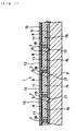
- Fig. 1 shows an example of a cross-sectional structure of an integrated thin-film solar battery 1 in accordance with the present invention.
- an integrated thin-film solar battery 1 having a plurality of unit elements 15 connected in series.
- a plurality of semiconductor layers 9 are disposed on a plurality of first electrode layers 5 which are divided into a plurality of regions on a substrate 3 in such a manner that each of the semiconductor layers 9 is formed on two adjacent first electrodes 5 and has a connection opening 7 on one of the two first electrodes 5.
- An electrically conductive layer 11 is formed in a region except for the connection opening 7 on each of the semiconductor layers 9.
- a second electrode layer 13 is disposed on each of the electrically conductive layers 11 in a state where the second electrode layer 13 is electrically connected to one of the two electrode layers 5 through the connection opening 7, thereby forming, as the unit element 15, a region interposed between the second electrode layer 13 and the other first electrode layer 5.
- a transparent electrically conductive film made of SnO 2 , ZnO, ITO or the like is deposited on the glass substrate 3 as the first electrode layer 5, and for integration, the first electrode layer 5 is then melted and cut off in correspondence with a plurality of power generation regions through the laser scribing technique, to thereby form a plurality of separation grooves 17.
- a plurality of strip-shaped power generation regions are formed along one direction of the substrate 3.
- a glass substrate of 910 x 455 x 4 mm 3 is used, and the surface resistance of the first electrode layer 5 is set to the order of 10 ohms.
- amorphous silicon hydride layer having a p-i-n structure is deposited on the entire surface of the first electrode layers 5 formed in correspondence with the plural power generation regions as a semiconductor layer 9 through the plasma CVD technique.
- the amorphous silicon hydride layer is produced in the manner stated bellow.
- silane gas is introduced into the chamber as the film formation gas, the reaction pressure is set to 0.2 to 0.7 Torr, and i-type amorphous silicon hydride is deposited to a thickness of approximately 3000 ⁇ through RF discharge.
- silane, phosphine (PH 3 ) and hydrogen (H 2 ) are introduced into the chamber as film formation gases, the reaction pressure is set to approximately 1.0 Torr, and n-type microcrystal silicon is deposited to a thickness of approximately 100 to 200 ⁇ through RF discharge.
- the first electrode layers 5 may be also have a n-i-p structure, or a tandem structure.
- the primary material of the semiconductor layer 9 may be not only amorphous silicon hydride but also amorphous silicon, multi-crystal or microcrystal, or a combination thereof.
- silicon may be replaced by silicon carbide, silicon germanium, germanium, a III-V group compound, II-VI group compound, I-III-VI group compound, or the like. Furthermore, it may be replaced by a combination of those compounds.
- An electrically conductive layer 11 is deposited on the semiconductor layers 9 sequentially without conducting a cleaning process through the sputtering technique.
- the substrate 3 on which the semiconductor layers 9 are deposited is introduced into a sputter chamber from which a gas is then exhausted to a high vacuum of 1 x 10 -6 Torr or higher.
- Argon gas (Ar) is introduced into the sputter chamber as a sputter gas, and ZnO doped with aluminum oxide (Al 2 O 3 ) is then deposited to a thickness of 800 to 1000 ⁇ under a pressure of 1 to 5 mTorr through RF discharge.
- the material of the electrically conductive layer 11 is a transparent electrically conductive material consisting of a metal oxide material such as SnO 2 or ITO. Furthermore, that material may be a laminate of those materials. What is important is that the electrically conductive layer 11 is deposited on the semiconductor layers 9 sequentially without conducting a cleaning process. More preferably, the electrically conductive layer 11 may be deposited sequentially, for example, within a device where a CVD chamber is coupled to the sputter chamber, without exposing the conductive layer 11 to the atmosphere after the deposition of the semiconductor layer 9.
- the semiconductor layer 9 and the electrically conductive layer 11 are melted and cut off simultaneously through the laser scribing technique, to thereby define a plurality of connection openings 7 adjacent to the separation grooves 17 of the first electrode layers 5, which have been already formed.
- a metal such as Al, Ag, Cr or the like is deposited on the electrically conductive layers 11 as a second electrode layer 13 through the sputtering technique or the vacuum vapor deposition technique as in the above manner.
- the second electrode layer 13 the electrically conductive layer 11 and the n-type microcrystal silicon layer in the vicinity of each of the connection openings 7 at an opposite side of the separation groove 17 of the first electrode layer 5 with respect to each of the connection openings 7 are removed through the laser scribing technique to thereby form an upper separation groove 19 so that the second electrode layer 13 is divided into a plurality of power generation regions.
- a plurality of unit elements 15 each consisting of a region which is interposed between the first electrode layer 5 and the second electrode layer 13 are connected in series and formed on the substrate 3.
- an electrically conductive layer 11 is deposited on the semiconductor layer 9 sequentially without conducting a cleaning process through the sputtering technique.
- the substrate 3 on which the semiconductor layers 9 are deposited is introduced into a sputter chamber from which a gas is then exhausted to a high vacuum of 1 x 10 -6 Torr or higher.
- Argon gas (Ar) is introduced into the sputter chamber as a sputter gas, and ZnO doped with aluminum oxide (Al 2 O 3 ) is then deposited to a thickness of approximately 500 ⁇ under a pressure of 1 to 5 mtorr through RF discharge.
- the material of the electrically conductive layer 11 may be a transparent electrically conductive material such as SnO 2 or ITO, or a laminate of those materials instead of ZnO. As above, what is important is that the electrically conductive layer 11 is deposited on the semiconductor layers 9 sequentially without conducting a cleaning process. More preferably, the electrically conductive layer 11 may be deposited sequentially, for example, within a device where a CVD chamber is coupled to the sputter chamber, without exposing the conductive layer 11 to the atmosphere after the deposition of the semiconductor layer 9.
- the semiconductor layer 9 and the electrically conductive layer 11 are melted and cut off simultaneously through the laser scribing technique, to thereby define a plurality of connection openings 7 adjacent to the separation grooves 17 of the first electrode layers 5, which have been already formed.
- a multi-layer film consisting of a transparent electrically conductive layer made of ZnO, SnO 2 , ITO or the like and a metal layer made of Al, Ag, Cr or the like is deposited on the electrically conductive layers 11 as a second electrode layer 13 through the sputtering technique or the vacuum vapor deposition technique as in the above manner.
- the substrate 3 on which the electrically conductive layers 11 are deposited is introduced into a sputter chamber from which a gas is then exhausted to a high vacuum of 1 x 10 -5 Torr or higher.
- Ar gas is introduced into the sputter chamber as a sputter gas, and ZnO doped with Al 2 O 3 is then deposited to a thickness of approximately 500 ⁇ under a pressure of 1 to 5 mtorr through RF discharge.
- the substrate 3 is introduced into a sputter chamber from which a gas is then exhausted to a high vacuum of 1 x 10 -5 Torr or higher.
- Ar gas is introduced into the sputter chamber as a sputter gas, and Ag is deposited to a thickness of approximately 3000 A as the metal layer through RF discharge under a pressure of 1 x 10 -5 Torr or higher. It is desirable to deposit ZnO and Ag sequentially without breaking the vacuum. However, if the vacuum is broken in the chamber once, then the layer may be deposited in another chamber or device.
- the metal layer may be of a multi-layer structure such as a laminate of, for example, Ag and Al, and the thickness may be set to at least 1000 ⁇ or more, although this depends on the kind of material.
- the RF sputtering may be replaced by DC sputtering.
- the second electrode layer 13 the electrically conductive layer 11 and the n-type microcrystal silicon layer in the vicinity of each of the connection openings 7 at an opposite side of the separation groove 17 of the first electrode layer 5 with respect to each of the connection openings 7 are removed through the laser scribing technique to thereby form an upper separation groove 19 so that the second electrode layer 13 is divided into a plurality of power generation regions.
- a plurality of unit elements 15 each consisting of a region which is interposed between the first electrode layer 5 and the second electrode layer 13 are connected in series and formed on the substrate 3.
- cleaning is conducted on the unit elements 15 in order to remove the remains melted and cut off by laser-scribing, and as occasion demands, an appropriate passivation layer made of epoxy resin or the like is coated on the final product.
- the thickness of ZnO deposited on the semiconductor layer 9 is set to a range of 600 to 1200 ⁇ , preferably, 800 to 1000 ⁇ . This is because light incident from the side of the glass substrate 3 is effectively reflected at the side of the second electrode layer 13 to obtain "a light shut-up effect".
- ZnO as the electrically conductive layer 11 is deposited to a thickness of 800 to 1000 ⁇ .
- the second electrode layer 13 is of a double-layer structure consisting of the transparent electrically conductive layer and the metal layer
- ZnO as the electrically conductive layer 11 and Ag as the second electrode layer 13 are deposited in a thickness of 500 ⁇ each to provide a thickness of 1000 ⁇ in total.
- the present invention can obtain the following secondary effects.
- Ag has a high reflection factor but not such an excellent adhesion to the underlayer.
- Ag contributes to an improvement of the conversion efficiency but the adhesive strength between Ag and the first electrode is weakened.
- the structure of the present invention is very useful in order to prevent the above problem. In other words, the unevenness of the surface of the electrically conductive layer 11 formed on the semiconductor layer 9 is increased, which can improve the adhesive strength between the electrically conductive layer 11 and the second electrode layer 13 deposited on the conductive layer 11.
- the electrically conductive layer 11 adheres to the second electrode layer 13 with a high adhesive strength on both sides of the connection opening 7, which can prevent the separation between the first electrode layer 5 and the second electrode layer 13 in the connection opening 7.
- one idea could be to roughen the surface of the first electrode layer 5.
- the unevenness of the surface of the first electrode layer 5 is increased, because the thickness of the semiconductor layer 9 is 3000 to 4000 ⁇ , there is a high risk of increasing a leak current flowing between the first electrode layer 5 and the second electrode layer 13. Hence, such an idea is undesirable.
- the unevenness of the surface of the electrically conductive layer 11 is increased can contribute to irregular reflection of incident light at the second electrode layer 13 side, and is very useful in the above-mentioned "light shut-up effect".
- the structure in which the second electrode layer 13 of the present invention is of the double-layer structure consisting of the transparent electrically conductive film and the metal layer is disclosed in Japanese Patent Examined Publication No. Sho 60-41878.
- a primary object of the structure disclosed in that publication is completely different from that of the present invention.
- such a structure does not contribute to an improvement in the adhesive strength between the above first electrode layer 5 and the second electrode layer 13 even from its structural viewpoint.
- the thin-film solar battery of the present invention has a structure in which the connection opening can be defined through the laser scribing technique after the semiconductor layer and the electrically conductive layer are sequentially deposited since the electrically conductive layer is formed in a region except for the connection opening on the semiconductor layer as described above. That is, the thin-film solar battery of the invention has a structure allowing it to be manufactured without the semiconductor layer being in direct contact with water used for cleaning or external air, which is different from the conventional thin-film solar battery.
- the FF value is remarkably improved in comparison with the conventional integrated thin-film solar battery, which can realize a remarkable improvement of the convention efficiency.
- the electrically conductive layer is made of a transparent electrically conductive film material such as SnO 2 , ZnO or ITO, no natural oxide film is produced on its surface by the cleaning process, and the interface between the electrically conductive layer and the second electrode layer is also kept in an excellent state. Furthermore, because alloying does not occur between the electrically conductive layer and the semiconductor layer, any factors that lead to the degradation of the FF value can be more completely removed, thereby being capable of more surely achieving an improvement in the conversion efficiency.
- a transparent electrically conductive film material such as SnO 2 , ZnO or ITO
- the semiconductor layer exists on both sides of each connection opening where the first electrode layer adheres to the second electrode layer, the unevenness of the surface of the electrically conductive layer is increased, and the adhesive strength between the electrically conductive layer and the second electrode layer deposited thereon is improved, even though the adhesive strength between the first electrode layer and the second electrode layer in the connection opening is weakened, the electrically conductive layer adheres to the second electrode layer with a high adhesive strength on both sides of the connection opening, thereby being capable of preventing the separation between the first electrode layer and the second electrode layer in the connection opening.
- the thin-film solar battery in accordance with the present invention is excellent from the viewpoint of reliability.
- the transparent electrically conductive material is used for the electrically conductive layer, light incident from the substrate side is effectively reflected on the second electrode layer side, thereby being capable of obtaining the "light shut-up effect" and contributing to an improvement in output current.
Description
Claims (16)
- An integrated thin-film solar battery (1) having a plurality of unit elements (15) connected in series, comprising:characterized in thata substrate (3);a plurality of first electrode layers (5) of transparent conductive oxide divided into a plurality of regions and formed on the substrate (3);a plurality of laminates each including a semiconductor layer (9) and a first electrically conductive layer (11) laminated on the semiconductor layer (9) disposed on said plurality of first electrode layers (5) in such a manner that each of the laminates is formed on two adjacent first electrodes (5) and has a connection opening (7) on one of the two first electrodes (5) said first electrically conductive layer being not formed in said connection opening; andsecond electrode layers (13) of metallic material disposed on each of the laminates in a state where the second electrode layers (13) are electrically connected to one of the two first electrode layers (5) through the connection opening (7) to form a region interposed between the second electrode layer (13) and the other first electrode layer as the unit element (15);
said first electrically conductive layer (11) consists of a transparent metal oxide material. - The integrated thin-film solar battery as claimed in claim 1, wherein said first electrically conductive layer (11) has a thickness in a range of 600 Å to 1200 Å (10 Å = 1 nm).
- The integrated thin-film solar battery as claimed in claim 1 or 2, further comprising a second electrically conductive layer of transparent metal oxide between the first transparent electrically conductive layer (11) and said second electrode layer (13).
- The integrated thin-film solar battery as claimed in claim 1, 2 or 3, wherein the second electrode layer (13) consists of silver.
- The integrated thin-film solar battery as claimed in any of claims 1 to 4, wherein the transparent metal oxide material of the first and second transparent electrically conductive layers (11) consists of zinc oxide, tin oxide or indium tin oxide.
- The integrated thin-film solar battery as claimed in any of claims 1 to 5, wherein the semiconductor layers (9) are doped with hydrogen.
- The integrated thin-film solar battery as claimed in any of claims 3 to 6, wherein the total thickness of said first and second transparent metal oxide layers is set to 1000 Å.
- A method of manufacturing an integrated thin-film solar battery (1) having a plurality of unit elements (15) connected in series, comprising the steps in the given order of:characterized in thatforming on a substrate (3) a plurality of first electrode layers (5) of transparent conductive oxide, wherein each of said layers (5) is the first layer of the plurality of unit elements (15);forming a laminate including a semiconductor layer (9) and a first electrically conductive layer (11) laminated on the semiconductor layer (9) covering said plurality of first electrode layers (5);forming connection openings (7). each of which penetrates the laminate and exposes a part of each first electrode layer (5);forming a second electrode layer (13) of metallic material on the laminate in a state where the second electrode layer (13) is electrically connected to each first electrode layer (5) through said connection opening (7); andforming isolation grooves (19) for dividing the second electrode layer (13) into a plurality of second electrode regions (13) in a state where the second electrode regions (13) are electrically connected to one of two adjacent first electrode layers (5) through the connection opening (7) to form a region interposed between the second electrode region (13) and the other first electrode layer as the unit element (15);
said first electrically conductive layer (11) is made of a transparent metal oxide material. - The method as claimed in claim 8, wherein the thickness of the first transparent electrically conductive layers (11) is set in a range of 600 Å to 1200 Å.
- The method as claimed in claim 8 or 9, wherein the semiconductor layers (9) are doped with hydrogen.
- The method as claimed in claims 8, 9 or 10, wherein the transparent electrically conductive layers (11) are formed without being exposed to water or external air after forming said semiconductor layers (9).
- A method as claimed in any of claims 8 to 11, further comprising the step of:forming a second electrically conductive layer of transparent metal oxide between the first transparent electrically conductive layer (11) and said second electrode layer (13).
- The method as claimed in any of claims 8 to 12, wherein the transparent metal oxide materials of the first and second transparent electrically conductive layers are made of zinc oxide, tin oxide or indium tin oxide.
- The method as claimed in any of claims 8 to 13, wherein said second electrode layers (13) are made of silver.
- The method as claimed in claim 14, wherein the second electrode layers (13) are formed by depositing said metal layer of silver in a vacuum state after depositing said first and/or second transparent metal oxide layers of zinc oxide, tin oxide or indium tin oxide.
- The method as claimed in any of claims 12 to 15, wherein the total thickness of said first and second transparent metal oxide layers is set to 1000 Å.
Applications Claiming Priority (3)
| Application Number | Priority Date | Filing Date | Title |
|---|---|---|---|
| JP14884795 | 1995-06-15 | ||
| JP14884795A JP3653800B2 (en) | 1995-06-15 | 1995-06-15 | Method for manufacturing integrated thin film solar cell |
| JP148847/95 | 1995-06-15 |
Publications (3)
| Publication Number | Publication Date |
|---|---|
| EP0749161A2 EP0749161A2 (en) | 1996-12-18 |
| EP0749161A3 EP0749161A3 (en) | 1998-07-15 |
| EP0749161B1 true EP0749161B1 (en) | 2004-12-22 |
Family
ID=15462073
Family Applications (1)
| Application Number | Title | Priority Date | Filing Date |
|---|---|---|---|
| EP96109504A Expired - Lifetime EP0749161B1 (en) | 1995-06-15 | 1996-06-13 | Integrated thin-film solar battery and method of manufacturing the same |
Country Status (6)
| Country | Link |
|---|---|
| EP (1) | EP0749161B1 (en) |
| JP (1) | JP3653800B2 (en) |
| KR (1) | KR970004102A (en) |
| AU (1) | AU704036B2 (en) |
| DE (1) | DE69634059T2 (en) |
| TW (1) | TW302553B (en) |
Cited By (2)
| Publication number | Priority date | Publication date | Assignee | Title |
|---|---|---|---|---|
| DE102009027852A1 (en) | 2009-07-20 | 2011-01-27 | Q-Cells Se | Thin-film solar module with improved interconnection of solar cells and method for its production |
| DE102009055675A1 (en) | 2009-11-25 | 2011-05-26 | Calyxo Gmbh | Photovoltaic module structures and method for producing an electrically conductive connection between two spaced-apart contact layers, in particular in the photovoltaic module structure |
Families Citing this family (18)
| Publication number | Priority date | Publication date | Assignee | Title |
|---|---|---|---|---|
| US6265652B1 (en) * | 1995-06-15 | 2001-07-24 | Kanegafuchi Kagaku Kogyo Kabushiki Kabushiki Kaisha | Integrated thin-film solar battery and method of manufacturing the same |
| US6077722A (en) * | 1998-07-14 | 2000-06-20 | Bp Solarex | Producing thin film photovoltaic modules with high integrity interconnects and dual layer contacts |
| US6468828B1 (en) * | 1998-07-14 | 2002-10-22 | Sky Solar L.L.C. | Method of manufacturing lightweight, high efficiency photovoltaic module |
| US6274804B1 (en) | 1999-07-28 | 2001-08-14 | Angewandte Solarenergie - Ase Gmbh | Thin-film solar module |
| JP2001044466A (en) * | 1999-07-29 | 2001-02-16 | Kanegafuchi Chem Ind Co Ltd | Method and system for cleaning integrated thin film solar cell |
| AU772539B2 (en) | 1999-07-29 | 2004-04-29 | Kaneka Corporation | Method for cleaning photovoltaic module and cleaning apparatus |
| EP2256824A3 (en) * | 1999-08-25 | 2012-09-12 | Kaneka Corporation | Thin film photoelectric conversion module and method of manufacturing the same |
| KR100416139B1 (en) * | 2001-04-04 | 2004-01-31 | 삼성에스디아이 주식회사 | Solar battery module |
| JP4573162B2 (en) * | 2004-09-16 | 2010-11-04 | 富士電機システムズ株式会社 | Method for producing transparent conductive film |
| JP2006339342A (en) * | 2005-06-01 | 2006-12-14 | Shin Etsu Handotai Co Ltd | Solar cell and method of manufacturing same |
| KR101144808B1 (en) * | 2008-09-01 | 2012-05-11 | 엘지전자 주식회사 | Manufacturing Method For Thin-Film Type Solar Cell And The Same thereof |
| EP2332177A4 (en) * | 2008-09-29 | 2012-12-26 | Thinsilicon Corp | Monolithically-integrated solar module |
| US20110284051A1 (en) * | 2009-01-29 | 2011-11-24 | Kyocera Corporation | Photoelectric Conversion Cell, Photoelectric Conversion Module, and Method for Manufacturing Photoelectric Conversion Cell |
| US8993877B2 (en) | 2009-06-23 | 2015-03-31 | Toray Engineering Co., Ltd. | Solar battery |
| JPWO2011132707A1 (en) | 2010-04-20 | 2013-07-18 | 京セラ株式会社 | Solar cell element and solar cell module using the same |
| JP5539081B2 (en) * | 2010-07-16 | 2014-07-02 | 株式会社カネカ | Manufacturing method of integrated thin film photoelectric conversion device |
| NL2007344C2 (en) * | 2011-09-02 | 2013-03-05 | Stichting Energie | Interdigitated back contact photovoltaic cell with floating front surface emitter regions. |
| KR101370554B1 (en) * | 2012-06-08 | 2014-03-10 | 재단법인대구경북과학기술원 | Thin film solar cell and method for producing thereof |
Family Cites Families (6)
| Publication number | Priority date | Publication date | Assignee | Title |
|---|---|---|---|---|
| JP60041878B2 (en) * | 1979-02-14 | 1985-09-19 | Sharp Kk | Thin film solar cell |
| GB2133617B (en) * | 1982-11-24 | 1987-07-08 | Semiconductor Energy Lab | Photoelectric conversion device and method of manufacture |
| JPS59172274A (en) * | 1983-03-18 | 1984-09-28 | Sanyo Electric Co Ltd | Manufacture of photovoltage device |
| US4755475A (en) * | 1986-02-18 | 1988-07-05 | Sanyo Electric Co., Ltd. | Method of manufacturing photovoltaic device |
| DE3714920C1 (en) * | 1987-05-05 | 1988-07-14 | Messerschmitt Boelkow Blohm | Method for producing a thin-layer solar cell arrangement |
| JPH06104465A (en) * | 1992-09-22 | 1994-04-15 | Fuji Electric Co Ltd | Thin film solar battery and manufacture thereof |
-
1995
- 1995-06-15 JP JP14884795A patent/JP3653800B2/en not_active Expired - Fee Related
-
1996
- 1996-05-09 TW TW085105502A patent/TW302553B/zh not_active IP Right Cessation
- 1996-06-11 KR KR1019960020779A patent/KR970004102A/en active Search and Examination
- 1996-06-12 AU AU55891/96A patent/AU704036B2/en not_active Ceased
- 1996-06-13 EP EP96109504A patent/EP0749161B1/en not_active Expired - Lifetime
- 1996-06-13 DE DE69634059T patent/DE69634059T2/en not_active Expired - Lifetime
Cited By (3)
| Publication number | Priority date | Publication date | Assignee | Title |
|---|---|---|---|---|
| DE102009027852A1 (en) | 2009-07-20 | 2011-01-27 | Q-Cells Se | Thin-film solar module with improved interconnection of solar cells and method for its production |
| WO2011009860A2 (en) | 2009-07-20 | 2011-01-27 | Q-Cells Se | Thin-layer solar module having improved interconnection of solar cells and method for the production thereof |
| DE102009055675A1 (en) | 2009-11-25 | 2011-05-26 | Calyxo Gmbh | Photovoltaic module structures and method for producing an electrically conductive connection between two spaced-apart contact layers, in particular in the photovoltaic module structure |
Also Published As
| Publication number | Publication date |
|---|---|
| JP3653800B2 (en) | 2005-06-02 |
| EP0749161A2 (en) | 1996-12-18 |
| JPH098337A (en) | 1997-01-10 |
| DE69634059T2 (en) | 2005-05-19 |
| AU5589196A (en) | 1997-01-02 |
| TW302553B (en) | 1997-04-11 |
| EP0749161A3 (en) | 1998-07-15 |
| KR970004102A (en) | 1997-01-29 |
| DE69634059D1 (en) | 2005-01-27 |
| AU704036B2 (en) | 1999-04-15 |
Similar Documents
| Publication | Publication Date | Title |
|---|---|---|
| US6265652B1 (en) | Integrated thin-film solar battery and method of manufacturing the same | |
| EP0749161B1 (en) | Integrated thin-film solar battery and method of manufacturing the same | |
| US6294722B1 (en) | Integrated thin-film solar battery | |
| EP1032051B1 (en) | Method for manufacturing thin film photovoltaic device | |
| US6300556B1 (en) | Solar cell module | |
| US6177711B1 (en) | Photoelectric conversion element | |
| JPH10256575A (en) | Photoelectric converter element, building material and generator | |
| JP3755048B2 (en) | Integrated thin film tandem solar cell and manufacturing method thereof | |
| US20120299142A1 (en) | Photoelectric conversion device | |
| US6348362B1 (en) | Manufacturing method of photovoltaic device | |
| JP3243229B2 (en) | Solar cell module | |
| JPH0832094A (en) | Thin film semiconductor solar cell and manufacture thereof | |
| JP4077456B2 (en) | Integrated thin film solar cell | |
| US20120090664A1 (en) | Photovoltaic device | |
| JPH09129903A (en) | Integrated thin film tandem solar battery and manufacture thereof | |
| JP3419108B2 (en) | Manufacturing method of thin film solar cell | |
| JP2846508B2 (en) | Photovoltaic element | |
| JP3243227B2 (en) | Solar cell module | |
| JP2004260013A (en) | Photoelectric converter and its manufacturing method | |
| JPH0883922A (en) | Solar cell and manufacture thereof | |
| JP2713847B2 (en) | Thin film solar cell | |
| JP3233388B2 (en) | Solar cell and method of manufacturing the same | |
| Hayashi et al. | ZnO-Ag sputtering deposition on a-Si solar cells | |
| JPH08222749A (en) | Method of manufacturing thin film solar battery | |
| JPH10200137A (en) | Integrated thin-film photoelectric converter and its manufacturing method |
Legal Events
| Date | Code | Title | Description |
|---|---|---|---|
| PUAI | Public reference made under article 153(3) epc to a published international application that has entered the european phase |
Free format text: ORIGINAL CODE: 0009012 |
|
| AK | Designated contracting states |
Kind code of ref document: A2 Designated state(s): DE FR |
|
| PUAL | Search report despatched |
Free format text: ORIGINAL CODE: 0009013 |
|
| AK | Designated contracting states |
Kind code of ref document: A3 Designated state(s): DE FR |
|
| 17P | Request for examination filed |
Effective date: 19980812 |
|
| 17Q | First examination report despatched |
Effective date: 20020729 |
|
| GRAP | Despatch of communication of intention to grant a patent |
Free format text: ORIGINAL CODE: EPIDOSNIGR1 |
|
| GRAS | Grant fee paid |
Free format text: ORIGINAL CODE: EPIDOSNIGR3 |
|
| GRAA | (expected) grant |
Free format text: ORIGINAL CODE: 0009210 |
|
| AK | Designated contracting states |
Kind code of ref document: B1 Designated state(s): DE FR |
|
| REF | Corresponds to: |
Ref document number: 69634059 Country of ref document: DE Date of ref document: 20050127 Kind code of ref document: P |
|
| ET | Fr: translation filed | ||
| PLBE | No opposition filed within time limit |
Free format text: ORIGINAL CODE: 0009261 |
|
| STAA | Information on the status of an ep patent application or granted ep patent |
Free format text: STATUS: NO OPPOSITION FILED WITHIN TIME LIMIT |
|
| 26N | No opposition filed |
Effective date: 20050923 |
|
| PGFP | Annual fee paid to national office [announced via postgrant information from national office to epo] |
Ref country code: DE Payment date: 20120607 Year of fee payment: 17 |
|
| PGFP | Annual fee paid to national office [announced via postgrant information from national office to epo] |
Ref country code: FR Payment date: 20120619 Year of fee payment: 17 |
|
| REG | Reference to a national code |
Ref country code: FR Ref legal event code: ST Effective date: 20140228 |
|
| REG | Reference to a national code |
Ref country code: DE Ref legal event code: R119 Ref document number: 69634059 Country of ref document: DE Effective date: 20140101 |
|
| PG25 | Lapsed in a contracting state [announced via postgrant information from national office to epo] |
Ref country code: DE Free format text: LAPSE BECAUSE OF NON-PAYMENT OF DUE FEES Effective date: 20140101 |
|
| PG25 | Lapsed in a contracting state [announced via postgrant information from national office to epo] |
Ref country code: FR Free format text: LAPSE BECAUSE OF NON-PAYMENT OF DUE FEES Effective date: 20130701 |