EP0748113A2 - Schmierkorrektur für einen CCD-Bildaufnehmer mit aktiven Bildelementen - Google Patents
Schmierkorrektur für einen CCD-Bildaufnehmer mit aktiven Bildelementen Download PDFInfo
- Publication number
- EP0748113A2 EP0748113A2 EP96420190A EP96420190A EP0748113A2 EP 0748113 A2 EP0748113 A2 EP 0748113A2 EP 96420190 A EP96420190 A EP 96420190A EP 96420190 A EP96420190 A EP 96420190A EP 0748113 A2 EP0748113 A2 EP 0748113A2
- Authority
- EP
- European Patent Office
- Prior art keywords
- smear
- estimation
- data
- image data
- correction
- Prior art date
- Legal status (The legal status is an assumption and is not a legal conclusion. Google has not performed a legal analysis and makes no representation as to the accuracy of the status listed.)
- Granted
Links
Images


Classifications
-
- H—ELECTRICITY
- H04—ELECTRIC COMMUNICATION TECHNIQUE
- H04N—PICTORIAL COMMUNICATION, e.g. TELEVISION
- H04N25/00—Circuitry of solid-state image sensors [SSIS]; Control thereof
- H04N25/60—Noise processing, e.g. detecting, correcting, reducing or removing noise
- H04N25/63—Noise processing, e.g. detecting, correcting, reducing or removing noise applied to dark current
-
- H—ELECTRICITY
- H04—ELECTRIC COMMUNICATION TECHNIQUE
- H04N—PICTORIAL COMMUNICATION, e.g. TELEVISION
- H04N25/00—Circuitry of solid-state image sensors [SSIS]; Control thereof
- H04N25/60—Noise processing, e.g. detecting, correcting, reducing or removing noise
- H04N25/62—Detection or reduction of noise due to excess charges produced by the exposure, e.g. smear, blooming, ghost image, crosstalk or leakage between pixels
- H04N25/625—Detection or reduction of noise due to excess charges produced by the exposure, e.g. smear, blooming, ghost image, crosstalk or leakage between pixels for the control of smear
-
- H—ELECTRICITY
- H04—ELECTRIC COMMUNICATION TECHNIQUE
- H04N—PICTORIAL COMMUNICATION, e.g. TELEVISION
- H04N25/00—Circuitry of solid-state image sensors [SSIS]; Control thereof
- H04N25/70—SSIS architectures; Circuits associated therewith
- H04N25/71—Charge-coupled device [CCD] sensors; Charge-transfer registers specially adapted for CCD sensors
Definitions
- the invention relates generally to the field of image sensors, and in particular to smear correction techniques employed within image sensors.
- CCD (charge coupled device) imagers are commonly used to capture digital images.
- the CCD imager is a solid state device which consists of an array of photosensors coupled with a CCD shift register.
- the photosensors convert incident photons to electrons resulting in a charge buildup in the photosensor which is proportional to the total amount of light incident over a given period of time.
- the integration time the time over which electrons are collected
- the charge from each photosensor is transferred to a corresponding location in an analog CCD shift register.
- the packets of charge now can be shifted sequentially onto a capacitor, generating a voltage which can be measured at the output of the imager.
- charge from the previous integration time period is shifted out of the device while charge is being integrated in the photosensors, resulting in a delay of one integration time period between integration and readout.
- CCD imagers typically fall into two categories: linear array and area array imagers.
- a linear array imager the pixels (individual photosensor locations are commonly referred to as a "pixels") are arranged in one long row. This type of device is used to capture one line of an image at a time. To capture an entire image, many lines must be captured in succession while either the object or the imager is translated past the other. Sometimes, more than one line of photosensors will be fabricated into the same device. When combined with color filtering, color capture of images is possible. Trilinear (R, G, B) imagers are made this way.
- the photosensors are arranged in a two dimensional pattern, allowing for capture of the entire image during one integration time period.
- Smear occurs when photo-generated electrons not captured by the potential well of the photosensor, become distributed in the substrate and are captured by the potential well of the shift register. The result is an extra charge “offset” which is added equally to each pixel shifted out of the device, and is proportional to the total amount of light incident on the entire array of photosensors. Part of the smear is contributed during integration, as smear charge is deposited into the shift register before photosensor charge is transferred, and part of the smear is contributed during readout of the shift register. Since charge transfer is delayed by one integration time period relative to charge integration, the smear for a given integration time period contains components from the current integration time period as well as the previous integration time period.
- Smear becomes visible in images when both dark and bright regions of the image are captured during a single line.
- the light from the bright regions causes smear to be added to all pixels, including those which should be dark.
- the smear offset for a given line must be measured or calculated and then subtracted from each pixel's readout value.
- a common approach involves the use of "light shield" pixels.
- a light shield pixel is an extra pixel which is fabricated on the device but is completely masked so as not to receive light. Because light is never incident on the photosensor, any charge which accumulates must be from some undesirable source, such as smear. Therefore, the charge from the light shield pixel can be measured in the same way that charge is measured from all other "active" pixels, and then subtracted from the values of the active pixels.
- CCD imagers are inherently noisy devices. Sources of noise include: (1) Dark Noise, which is charge developed as a result of the thermal excitation of free electrons in the photosensor and shift register; (2) Shot Noise, which is a variation in the random arrival of photons as predicted by Poisson statistics; and ( 3) Electronics Noise, which can be any noise introduced by the processing and measuring electronics.
- error average error single /sqrt(number of measurements)
- a smear correction circuit for elimination of smear error within image sensing devices comprising:
- the new approach has been developed which eliminates the need for a large number of light shield pixels, and reduces the error in the smear offset to extremely small levels.
- This approach relies on the fact that the smear offset is linearly proportional to the total amount of light incident on the imager during its integration time.
- the signal values from all active pixel locations are accumulated or averaged, and multiplied by a predetermined scaling factor to produce an estimate of the actual smear offset.
- the scaling factor is simply the worst case smear expressed as a percentage of the maximum signal value, usually between 0 and 10%. Since the number of active pixels is usually large, the error in the accumulated value is very small, even though the error in each individual pixel measurement is larger on average than that of a light shield pixel (because of the additional shot noise component in an illuminated pixel).
- Ws is the worst case scaling factor
- Ns is the amount of shot noise
- the present invention has the advantage of eliminating the need for a large number of light shield pixels and reducing smear error to extremely small levels.
- Fig. 1 is a block diagram of the data processing path.
- Fig. 2 is a graph illustrating the typical pixel response function.
- Fig. 3 is a diagram of a linear CCD imager.
- Fig. 4 is a diagram of a typical scan using the imager of Fig. 3.
- Fig. 5 is an alternative to the processing path of Fig. 1.
- Fig. 6 is another alternative to the processing path of Fig. 1.
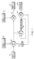
- the image data processing path includes active pixel smear correction. Two types of image data correction are used to obtain the final smear corrected data. As shown in Fig. 1, dark correction 30 and gain correction 60 are directly combined with the image data between the image data input 10 and the image data output 70.
- the preferred embodiment shown in Fig. 1 is only one possible configuration that can be used to acheive the results of the present invention.
- Image Data input 10 provides digitized data, typically from a CCD imager.
- dark correction and smear correction takes place by combining these values with the data from the image data input 10.
- the values used for dark correction come from the dark correction 30.
- the dark correction 30 is a storage device that has been previously loaded with dark corrections values during a calibration cycle.
- the smear correction value for an entire line is provided by latch 40. This value was calculated during the previous line.
- Image data which has been corrected for dark offset and smear offset is sent to the gain correction multiplier 50 and active pixel accumulation 80.
- Active pixel accumulation 80 sums the image data values from all active pixels, multiplies the accumulated value by the smear scaling factor 100 at multiplier 90, and holds the result in latch 40 for use on the next line. Active pixel accumulation occurs before gain correction, so that the contribution from each active pixel towards the total illumination is weighted equally.
- Gain correction is performed at gain correction multiplier 50 by using gain correction values from gain correction storage 60, providing output image data 70 for use by subsequent image processing stages.
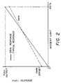
- Fig. 2 shows the typical response function of an individual pixel.
- the dashed line shows the typical response.
- the solid line shows the ideal (desired) response.
- Dark and gain correction are used to produce the desired response from a pixel which exhibits a non ideal response. As stated above, these values are determined during calibration periods.
- the photosensor will produce a small output signal, called the "dark offset”.
- the dark offset can be measured when no light is incident, and be subtracted from all subsequent measurements taken from that pixel. This process is called “dark correction”. If the variation in the dark offset among all pixels is small enough, one dark offset may be used for all pixels, otherwise a separate dark offset must be applied for each pixel.
- each pixel will produce a different output signal (referred to as the "bright point") because of variations in pixel response, illumination uniformity, etc.
- Signal output at all other illumination levels is assumed to fall on a straight line connecting the dark offset to the bright point. The slope of this line is the "gain" of the pixel.
- a gain correction factor can be calculated which will set the bright point to the desired value. All subsequent pixel values are multiplied by the gain correction factor. This process is called “gain correction”.
- image data 10 is digitized from a CCD imager.
- dark correction and smear correction take place.
- the dark correction storage 30 has been previously loaded with dark correction values during a calibration cycle.
- the smear correction for an entire line is provided by latch 40 with the value calculated during the previous line using the values from the equations discussed below.
- Image data that has been corrected for dark offset and smear offset is sent to gain correction 50 and active pixel accumulation 80.
- Active pixel accumulation 80 sums the image data values from all active pixels, multiplies the accumulated value by the smear scaling factor 100 at multiplier 90 and holds the result in latch 40 for use on the next line. Active pixel accumulation occurs before gain correction, so that the contribution from each pixel towards the total illumination is weighted equally.
- Gain correction is performed at gain correction multiplier 50, using gain correction values from gain correction storage 60, providing output image data 70 to subsequent processing stages.
- the per cent smear is determined by average values arrived at using the mathmatical representations discussed below which are best understood while referring to Fig. 3 in conjunction with Fig. 4.
- the numerator of Equation 1 is arrived at by taking the average amount of illumination for light shield pixels for all the light shield pixels during a calibration period.
- FIG. 3 is a functional representation of a linear CCD image sensor 110 having a number "N" image sensing elements comprising photodiodes 112 and CCD shift register 114.
- the photodiodes 112 have incident photons that generate electron hole pairs, within the photodiodes 112, which are transferred to CCD shift register 114.
- the first eight pixels and the last eight pixels, within image sensor 110, are light shield pixels 116, the pixels between the light shield pixels 116 are active pixels 118.
- Equation 2 if p(x, y) is used represent the value for a pixel location, denoted as "x”, within the image sensor 110, then for a multiple lines scanned by that image sensor 110, the value for pixel location "x", in any of the given lines, denoted as “y”, can be averaged. Assuming that L(x) denotes the average value for a pixel location, "x", over all the lines "y” scanned, then Equation 2 would accurately represent the average value, L(x), for that pixel location after line "y"has been scanned M+1 number of times. This relation can be seen by Equation 2 in conjunction with Fig. 4.
- Equation 3 the average light shield value of the light shield pixels contained in M+1 lines scanned as shown in Fig. 4, the average light shield value, LS, is given by Equation 3.
- AP is defined as the accumulation of pixel averages for the active pixels "x" within M+1 lines, this value is represented by AP as seen in Equation 4 below.
- the SSF from Equation 7 is loaded into the register for holding the scaling factor 100, as shown on Fig. 1, after calibration periods.
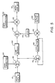
- a data processing path is shown having similarities to that of Fig. 1.
- the basic difference in the path shown in Fig. 5 is that line memory 130 will retain an entire line of data from summation circuit 20.
- This line of data is simultaneously parallel processed to generate a smear estimate as in Fig. 1.
- the smear estimate in Fig. 5 is used to correct for the same line by being made available to summation circuit 140 by latch 40 where it can provide smear correction for the data retained in line memory 130.
- FIG. 6 another alternative processing path provides an additional summation circuit 150 to provide smear corrected data to accumulator 80.
- the smear correction for the accumulated data is delayed by one line as in Fig. 1.
- the processing path in Fig. 6 provides more accuracy than the processing path as shown in Fig. 5.
Landscapes
- Engineering & Computer Science (AREA)
- Multimedia (AREA)
- Signal Processing (AREA)
- Transforming Light Signals Into Electric Signals (AREA)
Applications Claiming Priority (2)
| Application Number | Priority Date | Filing Date | Title |
|---|---|---|---|
| US08/462,414 US5661521A (en) | 1995-06-05 | 1995-06-05 | Smear correction of CCD imager using active pixels |
| US462414 | 1995-06-05 |
Publications (3)
| Publication Number | Publication Date |
|---|---|
| EP0748113A2 true EP0748113A2 (de) | 1996-12-11 |
| EP0748113A3 EP0748113A3 (de) | 1999-04-14 |
| EP0748113B1 EP0748113B1 (de) | 2002-07-24 |
Family
ID=23836350
Family Applications (1)
| Application Number | Title | Priority Date | Filing Date |
|---|---|---|---|
| EP96420190A Expired - Lifetime EP0748113B1 (de) | 1995-06-05 | 1996-05-24 | Schmierkorrektur für einen CCD-Bildaufnehmer mit aktiven Bildelementen |
Country Status (4)
| Country | Link |
|---|---|
| US (1) | US5661521A (de) |
| EP (1) | EP0748113B1 (de) |
| JP (1) | JPH08331463A (de) |
| DE (1) | DE69622475T2 (de) |
Cited By (7)
| Publication number | Priority date | Publication date | Assignee | Title |
|---|---|---|---|---|
| WO1999048286A3 (en) * | 1998-03-19 | 1999-12-16 | Koninkl Philips Electronics Nv | Image pick-up apparatus including a correction unit |
| EP0856990A3 (de) * | 1997-02-03 | 2000-05-10 | Trw Inc. | Korrektion für Frametransferausgabe |
| WO2006123828A1 (en) * | 2005-05-19 | 2006-11-23 | Casio Computer Co., Ltd. | Digital camera comprising smear removal function |
| EP1798956A1 (de) | 2005-12-16 | 2007-06-20 | Perkinelmer Singapore PTE Ltd. | Verfahren zur Verarbeitung von CCD-Daten und CCD-Bildaufnahmevorrichtung |
| EP1942659A1 (de) * | 2006-12-12 | 2008-07-09 | Axis AB | Verbessertes Verfahren zur Erfassung von Bilddaten |
| FR2951311A1 (fr) * | 2009-10-09 | 2011-04-15 | Trixell Sas | Procede de commande d'un dispositif photosensible |
| CN102281377A (zh) * | 2010-06-14 | 2011-12-14 | 佳能株式会社 | 图像读取装置及图像数据处理方法 |
Families Citing this family (15)
| Publication number | Priority date | Publication date | Assignee | Title |
|---|---|---|---|---|
| US6081608A (en) * | 1995-02-09 | 2000-06-27 | Mitsubishi Jukogyo Kabushiki Kaisha | Printing quality examining method |
| US6160578A (en) * | 1998-06-18 | 2000-12-12 | Redlake Imaging Corporation | High speed, increased bandwidth camera |
| JP4503740B2 (ja) * | 1999-10-14 | 2010-07-14 | オリンパス株式会社 | 撮像装置 |
| KR100405150B1 (ko) * | 2001-06-29 | 2003-11-10 | 주식회사 성진씨앤씨 | 시공간 적응적 잡음 제거/고화질 복원 방법 및 이를응용한 고화질 영상 입력 장치 |
| JP3762725B2 (ja) * | 2002-08-22 | 2006-04-05 | オリンパス株式会社 | 撮像システムおよび画像処理プログラム |
| JP2005229307A (ja) * | 2004-02-12 | 2005-08-25 | Sanyo Electric Co Ltd | 撮像装置、撮像装置の制御方法及び撮像装置の制御プログラム |
| CN100531402C (zh) * | 2004-10-15 | 2009-08-19 | 致伸科技股份有限公司 | 光电耦合器响应校正方法 |
| US7847979B2 (en) * | 2006-07-07 | 2010-12-07 | Eastman Kodak Company | Printer having differential filtering smear correction |
| KR100810344B1 (ko) * | 2006-10-10 | 2008-03-04 | 삼성전자주식회사 | 디지털 촬영 장치와 이를 이용한 스미어 현상 검출 및 보정방법 |
| US9053530B2 (en) | 2006-11-27 | 2015-06-09 | Google Inc. | Method for sliced inpainting |
| JP5335356B2 (ja) * | 2008-10-03 | 2013-11-06 | キヤノン株式会社 | 信号処理装置、信号処理方法、及び撮像装置 |
| TWI449412B (zh) * | 2009-05-27 | 2014-08-11 | Altek Corp | 影像資料補正方法 |
| JP6516204B2 (ja) * | 2016-01-19 | 2019-05-22 | 京セラドキュメントソリューションズ株式会社 | 画像読取装置、画像読取方法、画像形成装置及び制御プログラム |
| US11095839B1 (en) * | 2020-06-19 | 2021-08-17 | Shenzhen GOODIX Technology Co., Ltd. | Reducing smear through digital cancellation in image sensor |
| WO2023069916A1 (en) * | 2021-10-20 | 2023-04-27 | Princeton Infrared Technologies, Inc. | Buried photodetector with hetero structure as a gate |
Family Cites Families (13)
| Publication number | Priority date | Publication date | Assignee | Title |
|---|---|---|---|---|
| US4010319A (en) * | 1975-11-20 | 1977-03-01 | Rca Corporation | Smear reduction in ccd imagers |
| GB1526801A (en) * | 1976-01-08 | 1978-10-04 | British Broadcasting Corp | Compensating interference from solid state image sensing devices |
| JPS5814682A (ja) * | 1981-07-20 | 1983-01-27 | Sony Corp | 固体撮像装置 |
| NL8104103A (nl) * | 1981-09-04 | 1983-04-05 | Philips Nv | Televisie-opneeminrichting voorzien van een vaste-stof beeldopnemer. |
| JPS58156272A (ja) * | 1982-03-12 | 1983-09-17 | Sony Corp | スミア補正回路 |
| US4490744A (en) * | 1982-06-30 | 1984-12-25 | Rca Corporation | Smear reduction technique for CCD field-transfer imager system |
| US4594612A (en) * | 1985-01-10 | 1986-06-10 | Rca Corporation | Transfer smear reduction in line transfer CCD imagers |
| DE3821705A1 (de) * | 1988-06-28 | 1990-01-11 | Licentia Gmbh | Verfahren zur reduzierung des smeareffektes bei einer nach dem frame-transfer-prinzip arbeitenden videokamera |
| JP2660585B2 (ja) * | 1989-10-06 | 1997-10-08 | 富士写真フイルム株式会社 | 撮像装置 |
| US5086343A (en) * | 1990-05-11 | 1992-02-04 | Eastman Kodak Company | Method and apparatus for compensating for sensitivity variations in the output of a solid state image sensor |
| JPH04219063A (ja) * | 1990-05-15 | 1992-08-10 | Ricoh Co Ltd | 画像読取装置 |
| FR2662283B1 (fr) * | 1990-05-15 | 1992-07-24 | Thomson Trt Defense | Procede de correction d'images issues de capteur provoquant un bruit periodique, et dispositif de mise en óoeuvre. |
| US5121214A (en) * | 1990-06-29 | 1992-06-09 | The United States Of America As Represented By The United States Department Of Energy | Method for eliminating artifacts in CCD imagers |
-
1995
- 1995-06-05 US US08/462,414 patent/US5661521A/en not_active Expired - Lifetime
-
1996
- 1996-05-24 EP EP96420190A patent/EP0748113B1/de not_active Expired - Lifetime
- 1996-05-24 DE DE69622475T patent/DE69622475T2/de not_active Expired - Lifetime
- 1996-05-30 JP JP8137059A patent/JPH08331463A/ja active Pending
Cited By (14)
| Publication number | Priority date | Publication date | Assignee | Title |
|---|---|---|---|---|
| EP0856990A3 (de) * | 1997-02-03 | 2000-05-10 | Trw Inc. | Korrektion für Frametransferausgabe |
| WO1999048286A3 (en) * | 1998-03-19 | 1999-12-16 | Koninkl Philips Electronics Nv | Image pick-up apparatus including a correction unit |
| US8314864B2 (en) | 2005-05-19 | 2012-11-20 | Casio Computer Co., Ltd. | Digital camera comprising smear removal function |
| WO2006123828A1 (en) * | 2005-05-19 | 2006-11-23 | Casio Computer Co., Ltd. | Digital camera comprising smear removal function |
| US7733393B2 (en) | 2005-05-19 | 2010-06-08 | Casio Computer Co., Ltd. | Digital camera comprising smear removal function |
| CN101180869B (zh) * | 2005-05-19 | 2011-05-25 | 卡西欧计算机株式会社 | 具有拖尾消除功能的数字摄像机 |
| EP1798956A1 (de) | 2005-12-16 | 2007-06-20 | Perkinelmer Singapore PTE Ltd. | Verfahren zur Verarbeitung von CCD-Daten und CCD-Bildaufnahmevorrichtung |
| EP1942659A1 (de) * | 2006-12-12 | 2008-07-09 | Axis AB | Verbessertes Verfahren zur Erfassung von Bilddaten |
| FR2951311A1 (fr) * | 2009-10-09 | 2011-04-15 | Trixell Sas | Procede de commande d'un dispositif photosensible |
| WO2011042204A3 (fr) * | 2009-10-09 | 2011-06-16 | Trixell Sas | Procede pour la reduction du bruit dans le signal d'image d'un dispositif photosensible |
| US8994853B2 (en) | 2009-10-09 | 2015-03-31 | Commissariat A L'energie Atomique Et Aux Energies Alternatives | Method for controlling a light-sensitive device |
| CN102281377A (zh) * | 2010-06-14 | 2011-12-14 | 佳能株式会社 | 图像读取装置及图像数据处理方法 |
| CN102281377B (zh) * | 2010-06-14 | 2014-07-02 | 佳能株式会社 | 图像读取装置及图像数据处理方法 |
| US8953233B2 (en) | 2010-06-14 | 2015-02-10 | Canon Kabushiki Kaisha | Image reading apparatus and image data processing method |
Also Published As
| Publication number | Publication date |
|---|---|
| EP0748113B1 (de) | 2002-07-24 |
| US5661521A (en) | 1997-08-26 |
| DE69622475T2 (de) | 2003-02-20 |
| EP0748113A3 (de) | 1999-04-14 |
| DE69622475D1 (de) | 2002-08-29 |
| JPH08331463A (ja) | 1996-12-13 |
Similar Documents
| Publication | Publication Date | Title |
|---|---|---|
| US5661521A (en) | Smear correction of CCD imager using active pixels | |
| EP3499873B1 (de) | Korrektur für schwankungen in der empfangenen lichtmenge in einem photonenzählenden bildsensor | |
| CN101361360B (zh) | 用于在使用光学黑色像素及束缚像素的成像器中设定黑色电平的方法及设备 | |
| EP1968307B1 (de) | Bilderfassungsvorrichtung und Bilderfassungssystem | |
| JP4351658B2 (ja) | メモリ容量低減化方法、メモリ容量低減化雑音低減化回路及びメモリ容量低減化装置 | |
| GB2328338A (en) | Temperature dependent dark current correction in imaging apparatus | |
| US7196725B1 (en) | Image reading apparatus and computer readable storage medium | |
| US8089533B2 (en) | Fixed pattern noise removal circuit, fixed pattern noise removal method, program, and image pickup apparatus | |
| US20040051797A1 (en) | Fixed pattern noise removal in CMOS imagers across various operational conditions | |
| EP4346225B1 (de) | Lawinenphotoelektrische umwandlungsvorrichtung, steuerungsverfahren und speichermedium | |
| US6522355B1 (en) | Digital nonuniformity correction for image sensors | |
| EP0660596B1 (de) | Digitale Schaltung für automatische Korrektur der Schwarzschattierungseffekte in Kameras | |
| US6295383B1 (en) | Intensity correction in an optical scanner | |
| US20040189836A1 (en) | System and method for compensating for noise in image information | |
| US7991239B2 (en) | Methods, systems and apparatuses for imager row-wise noise correction | |
| JP2003259234A (ja) | Cmosイメージセンサ | |
| JP3642666B2 (ja) | 測光システム | |
| JPH0530350A (ja) | 固体撮像装置 | |
| JP2000228745A (ja) | 映像信号処理装置および映像信号処理方法、画像処理装置および画像処理方法、ならびに撮像装置 | |
| US5963251A (en) | Frame transfer readout correction | |
| JPH09181977A (ja) | 固体撮像装置 | |
| Kamberova | Understanding the systematic and random errors in video sensor data | |
| WO1995027367A1 (en) | Improvements relating to sensor arrays | |
| CN121078337A (zh) | 图像处理方法、成像方法、系统、电子设备和存储介质 | |
| JP3157455B2 (ja) | スミア除去回路 |
Legal Events
| Date | Code | Title | Description |
|---|---|---|---|
| PUAI | Public reference made under article 153(3) epc to a published international application that has entered the european phase |
Free format text: ORIGINAL CODE: 0009012 |
|
| AK | Designated contracting states |
Kind code of ref document: A2 Designated state(s): DE FR GB |
|
| PUAL | Search report despatched |
Free format text: ORIGINAL CODE: 0009013 |
|
| AK | Designated contracting states |
Kind code of ref document: A3 Designated state(s): DE FR GB |
|
| 17P | Request for examination filed |
Effective date: 19990924 |
|
| 17Q | First examination report despatched |
Effective date: 20000216 |
|
| GRAG | Despatch of communication of intention to grant |
Free format text: ORIGINAL CODE: EPIDOS AGRA |
|
| GRAG | Despatch of communication of intention to grant |
Free format text: ORIGINAL CODE: EPIDOS AGRA |
|
| GRAH | Despatch of communication of intention to grant a patent |
Free format text: ORIGINAL CODE: EPIDOS IGRA |
|
| GRAH | Despatch of communication of intention to grant a patent |
Free format text: ORIGINAL CODE: EPIDOS IGRA |
|
| GRAA | (expected) grant |
Free format text: ORIGINAL CODE: 0009210 |
|
| AK | Designated contracting states |
Kind code of ref document: B1 Designated state(s): DE FR GB |
|
| REG | Reference to a national code |
Ref country code: GB Ref legal event code: FG4D |
|
| REF | Corresponds to: |
Ref document number: 69622475 Country of ref document: DE Date of ref document: 20020829 |
|
| ET | Fr: translation filed | ||
| PLBE | No opposition filed within time limit |
Free format text: ORIGINAL CODE: 0009261 |
|
| STAA | Information on the status of an ep patent application or granted ep patent |
Free format text: STATUS: NO OPPOSITION FILED WITHIN TIME LIMIT |
|
| 26N | No opposition filed |
Effective date: 20030425 |
|
| PGFP | Annual fee paid to national office [announced via postgrant information from national office to epo] |
Ref country code: GB Payment date: 20050406 Year of fee payment: 10 |
|
| PGFP | Annual fee paid to national office [announced via postgrant information from national office to epo] |
Ref country code: FR Payment date: 20050517 Year of fee payment: 10 |
|
| PGFP | Annual fee paid to national office [announced via postgrant information from national office to epo] |
Ref country code: DE Payment date: 20050531 Year of fee payment: 10 |
|
| PG25 | Lapsed in a contracting state [announced via postgrant information from national office to epo] |
Ref country code: DE Free format text: LAPSE BECAUSE OF THE APPLICANT RENOUNCES Effective date: 20060222 |
|
| PG25 | Lapsed in a contracting state [announced via postgrant information from national office to epo] |
Ref country code: GB Free format text: LAPSE BECAUSE OF NON-PAYMENT OF DUE FEES Effective date: 20060524 |
|
| GBPC | Gb: european patent ceased through non-payment of renewal fee |
Effective date: 20060524 |
|
| REG | Reference to a national code |
Ref country code: FR Ref legal event code: ST Effective date: 20070131 |
|
| PG25 | Lapsed in a contracting state [announced via postgrant information from national office to epo] |
Ref country code: FR Free format text: LAPSE BECAUSE OF NON-PAYMENT OF DUE FEES Effective date: 20060531 |