CROSS-REFERENCE TO RELATED APPLICATIONS
This application is a National Stage of International patent application PCT/EP2010/006187, filed on Oct. 11, 2010, which claims priority to foreign French patent application No. FR 0904847, filed on Oct. 9, 2009, the disclosures of which are incorporated by reference in their entirety.
FIELD OF THE INVENTION
The present invention relates to a method of controlling a photosensitive device comprising a matrix of photosensitive points which are produced for example by techniques for depositing semi-conducting materials. It applies essentially, but not exclusively, to photosensitive devices used for the detection of radiological images.
BACKGROUND
Technologies using semi-conducting materials such as for example:
-
- hydrogenated amorphous silicon (aSiH), on insulating glass supports,
- CMOS on crystalline silicon substrate,
- charge-coupled circuits (CCD) on crystalline silicon substrate,
make it possible to produce matrices of photosensitive points that are able to produce an image on the basis of visible or near-visible radiation. These matrices can nonetheless be used within the framework of the detection of radiological images. Accordingly, it suffices to interpose a scintillator screen between the X-ray radiation and the matrix so as to convert the X-ray radiation into luminous radiation in the band of wavelengths to which the photosensitive points are sensitive. The X-rays can also be converted directly into electrical charge by virtue of a photoconducting material (e.g.: a-Se, CdTe, PbO, PbI2, etc.). In this case, the photosensitive points each comprise a charge storage capacitor.
The photosensitive points which form these matrices generally comprise a photosensitive element associated with an element fulfilling an on/off switch function. The photosensitive point is mounted between a row conductor and a column conductor. According to requirements, the photosensitive device then comprises a plurality of photosensitive points disposed as a matrix or strip.
The photosensitive element commonly consists of a diode, mounted in series with the on/off switch element. The on/off switch element may be for example a so-called switching diode whose “passing” or “on” state corresponds to the bias which turns it on in the forward direction, and whose “blocked” or “off” state corresponds to the reverse bias thereof. The two diodes are mounted with opposite directions of conduction, in a so-called “head-to-tail” configuration. Such an arrangement is well known, notably from French patent application 86 14058 (Publication No. 2 605 166) in which are described a matrix of photosensitive points of the type with two diodes in “head-to-tail” configuration, a method for reading the photosensitive points and a way of producing a photosensitive device such as this.
The column conductors are linked to a reading circuit converting the charge accumulated in the photosensitive elements into signals and delivering these signals as output. More particularly, the reading circuit can comprise several stages. Among these stages, a first stage can convert the charge into analog signals; a second stage can amplify these signals; a third stage can multiplex the signals so as to deliver “in series” and row after row as output from the reading circuit, a multiplexed signal comprising the signals representative of the charge accumulated in the photosensitive elements; and a fourth stage can convert the analog multiplexed signal into a digital signal. Like any electronic device, the reading circuit introduces electronic noise that gets added to the signals representative of the accumulated charge and limits the signal-to-noise ratio. In this instance, noise is generated at each stage of the reading circuit, and possibly further on in the image acquisition chain. More generally, noise is introduced at each modification or transformation of an analog signal, until this signal is converted into a digital signal. The noise is particularly troublesome insofar as the signals arising from the first stage may have a very small amplitude for certain modes of image acquisition, in particular when the X-ray radiation exposure time is small. The signal-to-noise ratio is then very small, for example close to unity, and the so-called useful signal, that is to say that representative of the charge accumulated in the photosensitive elements, may be difficult to extract from the overall signal, that is to say from the signal comprising at one and the same time the useful signal and the noise.
The generation of noise by the image acquisition chain may be limited by the design of the photosensitive device. However, noise generation depends greatly on the mode of use of the photosensitive device, notably the time for which the photosensitive points are exposed, the speed of reading the charge and the amplification gain applied to the signals. Thus, during the design of the photosensitive device, a compromise must be made between the various possible modes of use.
A solution for decreasing the noise generated during the transfer of the charge accumulated in the various photosensitive points to a charge amplifier is known from the French patent application published under the number FR 2 625 593. This patent describes a method for reading passive photosensitive points where the following is performed N times successively: a transfer of the charge present on each column of the matrix to intermediate storage zones, a duplication of this charge, a column-wise averaging of the duplicated charge and a restoral to the columns of the original charge. The charge averages are thereafter transferred to the following stage. The noise introduced during each transfer to the intermediate storage zones is generally decorrelated from the other noise. The averaging therefore makes it possible to partially cancel said noise. However, though the solution described in this patent does indeed make it possible to globally reduce the noise introduced by the image acquisition chain, it is solely at the level of the transfer of charge between the photosensitive points and the charge amplifier. The noise introduced at all the other stages of the image acquisition chain is not reduced. Moreover, the solution described in this patent applies only to the reading of passive photosensitive points, that is to say photosensitive points where the charge is converted into voltages in the reading circuit and not directly in the photosensitive points, as is the case for active photosensitive points.
SUMMARY OF THE INVENTION
An aim of the invention is notably to alleviate all or some of the aforementioned drawbacks. For this purpose, the subject of the invention is a method of controlling a photosensitive device comprising a matrix of photosensitive points organized in rows and columns, the method comprising a step of acquiring an image in the course of which each photosensitive point is able to accumulate a charge and a step of reading this image, the reading step comprising a prior sub-step of converting the charge accumulated at the various photosensitive points into analog signals representative of this charge and a sub-step of processing these analog signals with a view to obtaining a digital image, the method being characterized in that the processing sub-step is repeated N times for one and the same photosensitive point and for one and the same acquisition step with N an integer greater than or equal to two, and in that the reading step comprises a sub-step of averaging the N signals processed per photosensitive point so as to provide a single digital image per acquisition step.
According to a particular embodiment, the analog signals are voltages.
The processing sub-step can comprise:
-
- a conversion of the analog signals into digital signals;
- a multiplexing of the analog signals;
- a sampling/holding of the analog signals immediately preceding their multiplexing;
- an amplification of the analog signals or, if appropriate, of the digital signals.
According to a particular embodiment, each step of acquiring an image for which the photosensitive points are subjected to an exposure, called the useful image, is preceded by a step of acquiring an image for which the photosensitive points are not subjected to an exposure, called the offset image, and by a step of reading this offset image, the step of reading the offset image being identical to the step of reading the useful image, the useful image being corrected as a function of the offset image.
In a first variant, the processing sub-step is repeated N times for one and the same row before considering the next row.
In a second variant, the processing sub-step considers each row in succession before being repeated.
According to a first embodiment, the analog signals representative of the charge of all the photosensitive points are reset to zero after the N repetitions for each photosensitive point of the processing sub-step.
According to a second embodiment, the analog signals representative of the charge of all the photosensitive points of the row considered are reset to zero before considering the next row.
The advantage of the invention is notably that it makes it possible to decrease the noise generated over almost the entire image acquisition chain. In particular, the noise generated as soon as the charge is converted into analog signals may be reduced.
BRIEF DESCRIPTION OF THE DRAWINGS
The invention will be better understood and other advantages will become apparent on reading the detailed description of an embodiment given by way of example, which description is offered in relation to appended drawings which represent:
FIG. 1, a first exemplary passive photosensitive device to which the invention can be applied;
FIG. 2, a second exemplary passive photosensitive device to which the invention can be applied;
FIG. 3, an exemplary active photosensitive device to which the invention can be applied;
FIG. 4, possible steps for the method according to the invention;
FIGS. 5, 6 and 7, timecharts showing various possibilities for sequencing the processing operations and resets to zero of the signals for the various rows of a matrix of a photosensitive device.
DETAILED DESCRIPTION
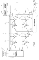
FIG. 1 represents a simplified diagram of a photosensitive device 1 comprising a matrix 2 organized in a conventional manner. The matrix 2 comprises photosensitive points P1 to P9, each formed by a photosensitive diode Dp and a switching diode Dc mounted in series according to a head-to-tail configuration. The matrix comprises row conductors Y1 to Y3 crossed with column conductors X1 to X3, with at each crossover, a photosensitive point P1 to P9 connected between a row conductor Y1 to Y3 and a column conductor X1 to X3. The photosensitive points P1 to P9 are thus arranged according to rows L1 to L3 and columns Cl1 to Cl3. They are also called pixels.
In the example of FIG. 1, only three rows and three columns are represented which define nine photosensitive points P1 to P9, but such a matrix can have a much larger capacity, of possibly as much as several million points. It is commonplace for example to produce such matrices having photosensitive points arranged as 3000 rows and 3000 columns (in an area of the order of 40 cm×40 cm), or indeed arranged as a single row and several columns so as to constitute a detection strip, or else arranged as a single row and a single column so as to constitute a single photosensitive point.
The photosensitive device 1 comprises a row control circuit 3, some of whose outputs SY1, SY2 and SY3 are linked respectively to the row conductors Y2 and Y3. The row control circuit 3 has various elements, not represented, such as for example, a clock circuit, switching circuits, and a shift register, which allow it to carry out sequential addressing of the row conductors Y1 to Y3. The photosensitive device 1 furthermore comprises a voltage source 4, delivering to the row control circuit 3 a voltage VP1 serving to define the amplitude of bias pulses applied to the row conductors Y1, Y2 and Y3 and a voltage source 13, delivering to the row control circuit 3, a voltage VP2 serving to define the amplitude of reading pulses applied to the row conductors Y1, Y2 and Y3. These two sources of voltages 4 and 13 can optionally be merged into one.
In each photosensitive point P1 to P9, the two diodes Dp and Dc are linked together either by their anode, as represented in FIG. 1, or by their cathode. The cathode of the photodiode Dp is linked to a column conductor X1 to X3, and the cathode of the switching diode Dc is linked to a row conductor Y1 to Y3.
In the image acquisition or image capture phase, that is to say during the phase of exposure of the matrix 2 to a so-called “useful” luminous signal, the two diodes Dp and Dc of each photosensitive point P1 to P9 are reverse biased. In this state, they each constitute a capacitance. It should be noted that generally the two diodes Dp and Dc are designed so that the capacitance exhibited by the photodiode Dp is the higher, of the order for example of 50 times.
During the acquisition of an image, charge is engendered in the photodiode Dp by the exposure of the photosensitive point P1 to P9 to which it belongs. This charge, the quantity of which is dependent on the exposure intensity, accumulates at a point A on the node formed at the point joining the two diodes Dp and Dc. The reading of the photosensitive points P1 to P9 is performed row by row, simultaneously for all the photosensitive points linked to one and the same row conductor Y1 to Y3. For this purpose, the row control circuit 3 applies a so-called amplitude reading pulse VP2 to each row conductor to Y3 addressed. The row conductors which are not addressed are kept at a reference potential Vr or quiescent potential. This reference potential Vr is for example earth. It may be the same potential as that which is applied to the column conductors X1 to X3.
The possible accumulation of charge at the point A of a photosensitive point P1 to P9 causes a decrease in the voltage at this point, that is to say a decrease in the reverse bias voltage of the photodiode Dp. With certain modes of operation, the effect of applying the reading pulse to a row conductor Y1 to Y3 is to restore to the potential of the point A of all the photosensitive points linked to this row conductor, the bias level that it possessed before exposure to the useful luminous signal. This results in a flow in each of the column conductors X1 to X3 of a current proportional to the charge accumulated at the corresponding point A.
The column conductors X1 to X3 are linked to a reading circuit CL comprising, in the example of FIG. 1, an integrator circuit 5, a multiplexer circuit 6, a video amplifier 7 and an analog-digital converter 8. The integrator circuit 5 comprises as many amplifiers as column conductors X1 to X3 i.e., in the example of FIG. 1, three amplifiers G1 to G3. It furthermore comprises an integration capacitor C1 to C3 and an on/off switch element I1 to I3 for each amplifier G1 to G3. Each column conductor X1 to X3 is linked to a negative input “−” of an amplifier G1 to G3 mounted as an integrator. An integration capacitor C1 to C3 is mounted between the negative input “−” and an output S1 to S3 of each amplifier. The second input “+” of each amplifier G1 to G3 is linked to a potential which, in the example of FIG. 1, is the reference potential Vr. Accordingly, this potential is imposed on all the column conductors X1 to X3. Each amplifier comprises a so-called reset-to-zero on/off switch element I1 to I3 mounted in parallel with each integration capacitor C1 to C3. The on/off switch elements I1 to I3 are for example transistors of the MOS type. The integrator circuit 5 thus transforms the charge flowing on the column conductors X1 to X3 into voltages.
The outputs S1 to S3 of the amplifiers G1 to G3 are linked to inputs Ent1 to Ent3 of the multiplexer circuit 6. The multiplexer circuit 6 is for example formed of a shift register with parallel inputs and series output possibly being of the charge-coupled type, more commonly called C.C.D. from the English expression “Charged-Coupled Device”. This conventional arrangement makes it possible to deliver “in series” and row after row (from L1 to L3), at the output of the multiplexer 6, voltages which represent the charge accumulated at the points A of all the photosensitive points P1 to P9. These voltages are called multiplexed signal SM.
The multiplexed signal SM can thereafter be amplified by the video amplifier 7 and converted into a digital signal SN by an analog-digital converter 8.
It should be noted that, in order to fulfill the on/off switch function which, in the example of FIG. 1, is achieved by the switching diode Dc, it is also known to use a transistor. The latter exhibits with respect to the diode a greater complexity of connection, but it offers advantages in the quality of its “on” state.
FIG. 2 schematically illustrates a photosensitive device 1′ which differs from that of FIG. 1 mainly in that it comprises a matrix 2′ in which the switching diodes Dc are replaced with transistors T, for example produced by techniques for depositing films in thin layers. Such transistors are known in the English literature by the term “Thin Film Transistor” (TFT). Techniques for depositing films in thin layers can also be used to produce the other elements of the matrices 2 and 2′ represented in FIGS. 1 and 2.
In the diagram shown in FIG. 2 by way of example, in each photosensitive point P1 to P9, the transistor T is linked by its source S to the cathode of the photodiode Dp, that is to say to the point A, its gate G is linked to the row conductor Y1 to Y3 to which the photosensitive point belongs, and its drain D is linked to the column conductor X1 to X3 to which the photosensitive point P1 to P9 belongs. The anodes of all the photodiodes Dp are linked to an output SY4 of the row control circuit 3. The output SY4 delivers a so-called bias voltage Vpolar, negative with respect to the reference potential Vr or earth, of the order for example of −5 volts. This bias voltage Vpolar serves to constitute the reverse bias of the photodiodes Dp. The row control circuit 3 receives for example this bias voltage from the voltage source 4.
For a better understanding of the general operation of the devices represented in FIGS. 1 and 2, reference may be made to the French patent applications published under the Nos. FR 2 760 585 and FR 2 605 166.
FIGS. 1 and 2 describe exemplary embodiments of photosensitive devices 1 and 1′ in which the photosensitive points P1 to P9 are termed passive. The invention applies, however, particularly well to photosensitive devices in which the photosensitive points are termed active, that is to say photosensitive points in which the charge accumulated during an image acquisition phase is converted into voltages at the level of the pixels and not outside the matrix in an integrator circuit.
FIG. 3 illustrates such a photosensitive device 1″ comprising a matrix 2″ of two rows L1 and L2 by two columns Cl1 and Cl2 of photosensitive points P1 to P4. The row control circuit 3 comprises two outputs SY1 and SY2 linked respectively to two row conductors Y1 and Y2. It furthermore comprises two outputs SRAZ1 and SRAZ2 linked respectively to two reset-to-zero conductors YRAZ1 and YRAZ2. Each photosensitive point P1 to P4 comprises a photodiode Dp and three transistors T1, T2 and T3. The first transistor T1 of each photosensitive point P1 to P4 is linked by its gate G to the reset-to-zero conductor YRAZ1 or YRAZ2 of the row L1 or L2 to which the photosensitive point P1 to P4 considered belongs, by its drain D to a voltage source 31 subjecting the drain D to a reset-to-zero potential VRAZ and by its source S to the cathode of the photodiode Dp belonging to the photosensitive point P1 to P4 considered. The anodes of all the photodiodes Dp are linked to a common potential, for example earth. The same point A may be defined between the source S of the transistor T1 and the cathode of the photodiode Dp. This point A is moreover linked to the gate G of the second transistor T2 of the same photosensitive point P1 to P4. The source S of this transistor T2 is linked to the source S of the third transistor T3 of the same photosensitive point P1 to P4 and the drains D of all the transistors T2 are linked to a voltage source 32 subjecting the drains D to a supply potential Vdd. The third transistor T3 of each photosensitive point P1 to P4 is moreover linked by its gate G to the row conductor Y1 or Y2 of the row L1 or L2 to which the photosensitive point P1 to P4 considered belongs and by its drain D to the column conductor X1 or X2 of the column Cl1 or Cl2 to which the photosensitive point P1 to P4 considered belongs.
The transistors T1 make it possible to reset the photosensitive points P1 to P4 into their original state, that is to say into the state that they had before being exposed to radiation. More particularly, the transistors T1 make it possible, when a reset-to-zero pulse is dispatched by the row control circuit 3 on a reset-to-zero conductor YRAZ1 or YRAZ2, to return the potential of the point A of all the photosensitive points P1 to P4 of the row L1 or L2 considered to the starting potential, in this instance the reset-to-zero potential VRAZ. The reset-to-zero pulses dispatched by the row control circuit 3 are for example provided by a voltage source 4″. The transistors T2 make it possible either to isolate the points A from the column conductors X1 and X2 when the transistors T3 are in the off state, or to copy (to within a constant) the values of the voltages at the points A onto the columns X1 and X2 when the transistors T3 are in the on state. The transistors T3 make it possible to select the row L1 or L2 for which it is desired to copy the signals at the points A onto the columns X1 and X2.
The reading of the photosensitive points P1 to P4 is also performed row by row. The row control circuit successively applies a reading pulse to each row conductor Y1 and Y2. The voltages at the point A of the photosensitive points P1 to P4 belonging to the row L1 or L2 which is read are then copied onto the column conductors X1 and X2 by way of the transistors T2. The voltages are copied to within a shift voltage.
In contradistinction to the photosensitive devices 1 and 1′ of FIGS. 1 and 2, the photosensitive device 1″ does not comprise any integrator circuit, the potential developed by the charge accumulated at the point A being copied at the level of the source S of the transistors T2. The column conductors X1 and X2 are linked directly to the inputs Ent1 and Ent2 of the multiplexer 6. The multiplexer 6 generally comprises an input stage consisting of a sample-and-hold stage. The multiplexer 6 delivers as output a multiplexed signal SM which can also be amplified by a video amplifier 7 and digitized by an analog-digital converter 8 so as to provide a digital signal SN.
FIG. 3 is offered with reference to a photosensitive device 1″ comprising solely two rows and two columns of photosensitive points. Of course, the invention applies to matrices of much more significant capacity. Furthermore, each photosensitive point can comprise more than three transistors and the supply voltage Vdd and reset-to-zero voltage VRAZ can differ for each photosensitive point. The electronics of the pixel can also be more complex and comprise for example a charge amplifier in place of the transistor T2.
In the photosensitive devices 1, 1′ and 1″ of FIGS. 1 to 3, it is considered that the charge is accumulated during exposure of the photosensitive points P1 to P9 by photodiodes Dp. However, this charge may be accumulated by any photosensitive element, for example phototransistors.
FIG. 4 illustrates possible steps for the method of controlling a photosensitive device such as for example described with reference to FIGS. 1, 2 and 3. The control method according to the invention can comprise a first step E1, termed the initialization step. According to a particular embodiment, adapted to the photosensitive device 1″ represented in FIG. 3, the photosensitive points P1 to P9 are reset to zero during this step E1; stated otherwise, they are reset to their original state. This particular embodiment is represented in FIGS. 5 and 6 described hereinbelow. For passive photosensitive devices 1 and 1′ such as represented in FIGS. 1 and 2, it is not the photosensitive points P1 to P9 which are reset to zero, but the voltages across the terminals of the integration capacitors C1 to C3 by way of the respective on/off switch elements I1 to I3. The control method comprises a step E2 of acquiring an image in the course of which each photosensitive point P1 to P9 is able to accumulate a charge and a step E3 of reading this image. In the course of step E2, the matrix 2, 2′ or 2″ is exposed to a useful luminous signal, originating for example from a scintillator receiving X-rays that have passed through a part of the body of a patient of whom it is desired to obtain a radiological image. Generally, the reading of the image is carried out row by row, but it can also be carried out pixel by pixel or simultaneously for all the pixels of the image. Step E3 comprises a prior sub-step E31 of converting the charge accumulated at the various photosensitive points of the row considered into analog signals representative of this charge, a sub-step E32 of processing these analog signals repeated N times for each photosensitive point P1 to P9 with N an integer greater than or equal to two, each processing sub-step E32 making it possible to obtain a row of a distinct digital image, and a sub-step E35 of averaging the N signals processed per photosensitive point P1 to P9. The N processed signals are averaged in relation to the photosensitive point P1 to P9 considered so as to provide at the end of the image acquisition chain, a single digital image per acquisition step. The value of N can notably be determined by the user as a function of the exposure time of the photosensitive points P1 to P9 and of the signal-to-noise ratio of the digital image that he desires to obtain. The value of N may be bounded by the time available between two image acquisitions. In a general manner, N is greater than 2, but so as not to slow down the reading rate excessively, N will preferably be chosen between 2 and 10.
Sub-step E31 is carried out in the photosensitive devices 1 and 1′ represented in FIGS. 1 and 2 by the integrator circuit 5 and, in the photosensitive device 1″ represented in FIG. 3, by the transistors T2. The analog signals representative of the charge are then voltages.
Sub-step E32 can comprise a multiplexing 322 of the analog signals so as to provide in series, for each processing sub-step E32, a multiplexed signal SM. The multiplexing 322 is for example carried out by the multiplexer 6 represented in FIGS. 1 to 3. Advantageously, the multiplexer 6 is preceded in the image acquisition chain by a sample/hold unit, not represented in these figures. The sampling/holding 321 then immediately precedes in the method according to the invention the multiplexing 322. According to a particular embodiment, the processing sub-step E32 comprises a digitization 324 of the analog signals, stated otherwise a conversion of the analog signals into digital signals. The analog signals can notably be digitized after the multiplexing 322 by the analog-digital converter 8. Still according to a particular embodiment, sub-step E32 comprises an amplification 323 of the analog and/or digital signals. The amplification 323 relates for example to the multiplexed signals SM. It may be carried out by the video amplifier 7. Although the description offered with reference to sub-step E32 presents a processing operation where the analog signals are firstly multiplexed, amplified, and then digitized, it must obviously be understood that the multiplexing 322, the amplification 323 and the digitization 324 may occur in a different order. Moreover, other processing operations may be carried out on the analog signals arising from the photosensitive points P1 to P9, such as amplifications and filterings. However, it is particularly advantageous to provide for a repetition of the whole of the part of the image acquisition chain which processes analog signals, including the digitization 324, because noise may be introduced at each stage of the image acquisition chain, in this instance during the sampling/holding 321, the multiplexing 322, the amplification 323 and the digitization 324. It is also possible to provide for a repetition of the whole of the image acquisition chain from the conversion of the charge into analog signals and up to the signals received by a display. The averaging of the signals is then performed as close as possible to the display in a part of the image acquisition chain generally comprising at least one microcontroller or a programmable logic circuit.
According to the invention, the processing sub-step E32 is repeated N times after each step E2 of acquiring an image, doing so for each row of photosensitive points. For each step E2, N multiplexed signals SM are therefore obtained per row. According to a particular embodiment, the repetition of sub-step E32 is obtained by way of a counter of readings, the value of which is denoted n. According to this particular embodiment, during the initialization step E1, the value n of the counter of readings is set to the value one. On completion of the processing sub-step E32, it is possible to determine in a sub-step E33 whether the value n of the counter is equal to the value N. If such is not the case, it is possible to increment the value n of the counter by one unit in a sub-step E34 and to repeat sub-step E32 in its entirety. If the value n of the counter is equal to the value N, the N processed signals obtained for each photosensitive point P1 to P9 are then averaged in a sub-step E35. During row-by-row processing, the N processed signals obtained originate from each photosensitive point of one and the same row, for example P1 to P3. Step E3 is repeated for each row (pixels P4 to P6, and then pixels P7 to P9). The averaging is for example an arithmetical or quadratic averaging. It can also be weighted as a function of the value n of the counter of readings or of an amplitude of certain signals. It is also possible to eliminate aberrant values of signals, for example lying outside predetermined brackets. The averaging can notably be performed on the N multiplexed and digitized signals. The signal obtained by the averaging sub-step E35 can then be utilized by the remainder of the image acquisition chain in the same manner as if it entailed a signal arising from a single processing sub-step E32.
The invention makes it possible to reduce the electronic noise introduced in the sub-step E32 of processing the analog signals insofar as the noise is at least partially decorrelated from other noise between two processing operations and is therefore partially cancelled out. More particularly, for completely decorrelated noise, the overall noise for N processing sub-steps E32 is divided by the square root of N (√{square root over (N)}) with respect to the noise which would be introduced for a single sub-step E32. Consequently, it is appreciated that for two processing sub-steps E32 (N=2), the noise is already reduced by more than 40 percent. For real-time processing, the processing sub-steps E32 are not repeated more than a certain number of times so as not to slow down the reading rate. The sub-steps E32 are for example repeated from 2 to 10 times for each row of photosensitive points (2≦N≦10).
On completion of the reading step E3, the signal may optionally undergo a post-processing in a step E4 and be utilized and/or displayed in a step E5. The post-processing can for example relate to a gain correction for each photosensitive point P1 to P9. A gain correction (pixel by pixel) is necessary insofar as the evolution of the ratio of the charge accumulated at a photosensitive point P1 to P9 to the integrated voltage for this charge does not correspond to the same linearity coefficient for all the photosensitive points P1 to P9.
According to a particular embodiment, each step E2 of acquiring a useful image, that is to say an image for which the photosensitive points P1 to P9 have been subjected to an exposure, is preceded by a step of acquiring an offset image, that is to say an image for which the photosensitive points P1 to P9 have not been subjected to an exposure, and by a step of reading this offset image. During the post-processing step E4, it is then possible to correct the useful image as a function of the offset image. An offset correction is generally necessary insofar as the semi-conducting components used in the photosensitive devices 1, 1′ and 1″, in particular the photodiodes Dp, the switching diodes Dc and the transistors T1, T2 and T3, are not all strictly identical. With the useful image encompassing the offset image, the correction of the useful image as a function of the offset image may be performed by pixel-by-pixel subtraction between the useful image and the offset image. In the case where there is no resetting to zero of the charge/voltage conversion stage, the offset correction consists of a correlated double sampling.
Still according to a particular embodiment, the step of reading the offset image is identical to step E3 of reading the useful image. Stated otherwise, the analog signals representative of the charge accumulated in the photosensitive points P1 to P9 in the absence of exposure and called offset signals are processed N times and then averaged pixel by pixel so as to decrease the noise generated by the processing sub-step E32 in the same manner as for the useful signals.
According to a particular embodiment, the control method according to the invention comprises several sequencings of the sub-steps E32 of processing and E35 of averaging, it being possible for the processing sub-steps E32 to differ according to the sequencing. By way of example, a first processing sub-step E32 can comprise a sampling/holding 321 and a multiplexing 322 of the analog signals and a second sub-step E32 can comprise an amplification 323 and a digitization 324 of the multiplexed signal SM, each sub-step E32 being repeated N times before the N signals which arise therefrom are respectively averaged in a first and in a second averaging sub-step E35.
FIGS. 5 and 6 illustrate, by timecharts, two different possibilities of sequencing the operations of processing the analog signals according to the rows of the matrix 2, 2′ or 2″. For the subsequent description, matrices of photosensitive points organized as NI rows by Nc columns are considered. In the timecharts, a high state is considered to be an active state and a low state is considered to be a passive state.
FIG. 5 illustrates a first possibility where the processing sub-step E32 is repeated N times for one and the same row before considering the next row. More precisely, according to this possibility, a row-by-row averaging of N signals originating from the pixels of one and the same row is performed. Stated otherwise, if a given row of pixels is considered, each reading circuit corresponding to a column (one also speaks of the foot of a column) collects N successive signals originating from the pixel situated in said row. It is known that, during the reading of a pixel, the potential read evolves toward an asymptotic value, the latter corresponding to the charge collected by the pixel. By collecting N successive samples of this potential, by means of the sample-and-hold unit 321, each successively collected sample approaches the asymptotic value. Thus, for each pixel of the row considered, the average of these N samples is more representative of the charge collected in the pixel, this in comparison with the case where the N readings are undertaken only by way of N complete acquisitions (on several rows), these N acquisitions being carried out without resetting the photosensitive points to zero. In this example, N has been chosen equal to three but any other integer value greater than or equal to two is of course possible. A first timechart C5RAZ presents the periods TRAZ of resetting the photosensitive points to zero. In relation to FIG. 3, the timechart C5RAZ illustrates a possible shape of signal for the reset-to-zero conductors YRAZ1 and YRAZ2. A second timechart C5expo presents the period Texpo of step E2 of acquiring an image, that is to say the period during which the photosensitive points are subjected to radiation. Three other timecharts C51, C52 and C5NI respectively represent the periods T51, T52 and T5NI during which the signals of the first, of the second and of the last row are processed by sub-step E32. In relation to FIG. 3, the timecharts C51 and C52 illustrate the signals that may possibly be applied to the row conductors Y1 and Y2, respectively. The timecharts C5RAZ, C5expo, C51, C52 and C5NI show that:
-
- each period Texpo is preceded by a period TRAZ;
- on completion of the period Texpo, the Nc signals of the first row are processed three times;
- after the last processing of the signals of the first row, the Nc signals of the second row are in their turn processed three times;
- and so on and so forth until the last row where the corresponding signals are processed three times.
Sub-step E35 and steps E4 and E5 can be carried out thereafter. A new step E2 of acquiring an image may be performed as soon as the last iteration of sub-step E32 of processing the last row finishes.
Of course, for a passive photosensitive device, the charge of the photosensitive points belonging to the row whose signals will be processed must be converted before the first processing sub-step E32, in accordance with the reading step E3 described with reference to FIG. 4.
FIG. 6 illustrates a second possibility of sequencing the operations of processing the analog signals where the processing sub-step E32 considers each row in succession before being repeated. In this example, N has been chosen equal to two. In FIG. 6, the timecharts C6RAZ of resetting the photosensitive points to zero and C6expo of exposing the photosensitive points are respectively identical to the timecharts C5RAZ and C5expo. Three other timecharts C61, C62 and C6NI respectively represent the periods T61, T62 and T6NI during which the signals of the first, of the second and of the last row are processed by sub-step E32. In contradistinction to the timecharts of FIG. 5, the timecharts C6RAZ, C6expo, C61, C62 and C6NI show that, on completion of the exposure period Texpo, the Nc signals of the first row are processed a first time, followed by the Nc signals of the second row, and so on and so forth until the last row where the corresponding signals are also processed a first time. The first row, the second row and the following rows are thereafter processed a second time, up to the last row. After the N iterations of sub-step E32 of processing the last row, the averaging steps E35, and then the post-processing step E4 and the utilization and/or display step E5 may be carried out. A new step E2 of acquiring an image can also be performed.
According to a particular embodiment, represented in FIGS. 5 and 6, the analog signals representative of the charge of all the photosensitive points are reset to zero after the N repetitions for each photosensitive point of the processing sub-step E32. Consequently, by considering two successive useful images, the resetting to zero of the analog signals according to the N repetitions of sub-step E32 for obtaining the first image corresponds to the resetting to zero preceding step E2 of acquiring the next image.
FIG. 7 illustrates, by timecharts, another particular embodiment of the method according to the invention with N equal to two. A first timechart C7expo presents the period Texpo of step E2 of acquiring an image. Three timecharts C71, C72 and C7NI respectively represent the periods T71, T72 and T7NI during which the signals of the first, of the second and of the last row are processed by sub-step E32. Three other timecharts C7RAZ1, C7RAZ2 and C7RAZNI illustrate the periods TRAZ1, TRAZ2 and TRAZNI during which the analog signals of the first, of the second and of the last row are respectively reset to zero. According to this particular embodiment, the analog signals representative of the charge of all the photosensitive points of the row considered are reset to zero before considering the next row. This embodiment is particularly adapted to a continuous exposure period Texpo or, at the very least, to one which is greater than the overall duration of processing of the signals arising from all the photosensitive points. In FIG. 7, it is considered that the step E2 of exposing the photosensitive points is performed in parallel with the reading step E3. The sequencing of the operations of processing the signals is performed in accordance with the possibility described with reference to FIG. 5, that is to say the processing sub-step E32 is repeated N times for one and the same row before considering the next row. On the other hand, after the N sub-steps E32 of processing the signals of the first row, these signals are reset to zero during a period TRAZ1. The signals of the second row are thereafter processed N times before being reset to zero during a period TRAZ2, and so on and so forth for all the rows of the matrix 2, 2′ or 2″, until the last row where the corresponding signals are processed N times before being reset to zero during a period TRAZNI. Then, steps E35, E4 and E5 are carried out. Thereafter, a new image can thus be acquired by a new reading step E3 where the signals of the various rows are processed in succession.
The invention makes it possible to reduce the noise generated by the image acquisition chain in a simple and economical manner, no hardware modification of the image acquisition chain being necessary. The number N of processing operations performed per photosensitive point can easily be adapted as a function of the desired signal-to-noise ratio and of the hardware resources of the image acquisition chain.