EP2486724B1 - Method for reducing noise in the image signal of an image sensor - Google Patents
Method for reducing noise in the image signal of an image sensor Download PDFInfo
- Publication number
- EP2486724B1 EP2486724B1 EP10810960.4A EP10810960A EP2486724B1 EP 2486724 B1 EP2486724 B1 EP 2486724B1 EP 10810960 A EP10810960 A EP 10810960A EP 2486724 B1 EP2486724 B1 EP 2486724B1
- Authority
- EP
- European Patent Office
- Prior art keywords
- image
- photosensitive
- line
- signals
- reading
- Prior art date
- Legal status (The legal status is an assumption and is not a legal conclusion. Google has not performed a legal analysis and makes no representation as to the accuracy of the status listed.)
- Active
Links
- 238000000034 method Methods 0.000 title claims description 26
- 238000012545 processing Methods 0.000 claims description 50
- 239000011159 matrix material Substances 0.000 claims description 19
- 238000012935 Averaging Methods 0.000 claims description 14
- 230000003321 amplification Effects 0.000 claims description 10
- 238000003199 nucleic acid amplification method Methods 0.000 claims description 10
- 238000006243 chemical reaction Methods 0.000 claims description 8
- 238000005070 sampling Methods 0.000 claims description 6
- 230000000903 blocking effect Effects 0.000 claims description 5
- 239000004020 conductor Substances 0.000 description 36
- 101000640246 Homo sapiens SCAN domain-containing protein 1 Proteins 0.000 description 7
- 102100033957 SCAN domain-containing protein 1 Human genes 0.000 description 7
- 230000000875 corresponding effect Effects 0.000 description 6
- 230000010287 polarization Effects 0.000 description 6
- 230000005855 radiation Effects 0.000 description 6
- 238000012937 correction Methods 0.000 description 5
- 238000010586 diagram Methods 0.000 description 4
- 230000010354 integration Effects 0.000 description 4
- 238000012805 post-processing Methods 0.000 description 4
- 238000012546 transfer Methods 0.000 description 4
- 238000011282 treatment Methods 0.000 description 4
- XUIMIQQOPSSXEZ-UHFFFAOYSA-N Silicon Chemical compound [Si] XUIMIQQOPSSXEZ-UHFFFAOYSA-N 0.000 description 3
- 239000003990 capacitor Substances 0.000 description 3
- 230000001276 controlling effect Effects 0.000 description 3
- 238000001514 detection method Methods 0.000 description 3
- 239000000463 material Substances 0.000 description 3
- 239000004065 semiconductor Substances 0.000 description 3
- 229910004613 CdTe Inorganic materials 0.000 description 2
- 229910021419 crystalline silicon Inorganic materials 0.000 description 2
- 238000013461 design Methods 0.000 description 2
- 238000012432 intermediate storage Methods 0.000 description 2
- 238000012986 modification Methods 0.000 description 2
- 230000004048 modification Effects 0.000 description 2
- 238000012163 sequencing technique Methods 0.000 description 2
- 239000000758 substrate Substances 0.000 description 2
- 238000007736 thin film deposition technique Methods 0.000 description 2
- 229920000297 Rayon Polymers 0.000 description 1
- 241001639412 Verres Species 0.000 description 1
- 238000009825 accumulation Methods 0.000 description 1
- 229910021417 amorphous silicon Inorganic materials 0.000 description 1
- 230000002596 correlated effect Effects 0.000 description 1
- 238000000151 deposition Methods 0.000 description 1
- 230000000694 effects Effects 0.000 description 1
- 238000005516 engineering process Methods 0.000 description 1
- 238000001914 filtration Methods 0.000 description 1
- 239000011521 glass Substances 0.000 description 1
- 238000003384 imaging method Methods 0.000 description 1
- 239000002964 rayon Substances 0.000 description 1
- 238000003860 storage Methods 0.000 description 1
- 239000010409 thin film Substances 0.000 description 1
- 230000009466 transformation Effects 0.000 description 1
Images


Classifications
-
- H—ELECTRICITY
- H04—ELECTRIC COMMUNICATION TECHNIQUE
- H04N—PICTORIAL COMMUNICATION, e.g. TELEVISION
- H04N5/00—Details of television systems
- H04N5/14—Picture signal circuitry for video frequency region
- H04N5/21—Circuitry for suppressing or minimising disturbance, e.g. moiré or halo
-
- H—ELECTRICITY
- H04—ELECTRIC COMMUNICATION TECHNIQUE
- H04N—PICTORIAL COMMUNICATION, e.g. TELEVISION
- H04N25/00—Circuitry of solid-state image sensors [SSIS]; Control thereof
-
- H—ELECTRICITY
- H04—ELECTRIC COMMUNICATION TECHNIQUE
- H04N—PICTORIAL COMMUNICATION, e.g. TELEVISION
- H04N23/00—Cameras or camera modules comprising electronic image sensors; Control thereof
- H04N23/80—Camera processing pipelines; Components thereof
- H04N23/81—Camera processing pipelines; Components thereof for suppressing or minimising disturbance in the image signal generation
-
- H—ELECTRICITY
- H04—ELECTRIC COMMUNICATION TECHNIQUE
- H04N—PICTORIAL COMMUNICATION, e.g. TELEVISION
- H04N25/00—Circuitry of solid-state image sensors [SSIS]; Control thereof
- H04N25/60—Noise processing, e.g. detecting, correcting, reducing or removing noise
Definitions
- the present invention relates to a method of controlling a photosensitive device comprising a matrix of photosensitive points, for example made by semiconductor material deposition techniques. It applies mainly, but not exclusively, to the photosensitive devices used for the detection of radiological images.
- the photosensitive spots that form these matrices generally comprise a photosensitive element associated with an element that performs a switch function.
- the photosensitive dot is mounted between an inline conductor and a column conductor.
- the photosensitive device then comprises a plurality of photosensitive points arranged in matrix or bar.
- the photosensitive element is commonly constituted by a diode, connected in series with the switch element.
- the switch element can be for example a so-called switching diode whose "closed” or “on” state corresponds to the polarization which puts it in direct conduction, and whose "open” or “blocked” state corresponds to its polarization in reverse. Both diodes are mounted with opposite directions of conduction, in a so-called "head-to-tail" configuration.
- the column conductors are connected to a read circuit converting the accumulated charges in the photosensitive elements into signals and delivering these signals at the output.
- the reading circuit may comprise several stages. Among these stages, a first stage can convert the charges into analog signals; a second stage can amplify these signals; a third stage can multiplex the signals so as to output "in series" and line after line at the output of the read circuit, a multiplexed signal comprising the signals representative of the charges accumulated in the photosensitive elements; and a fourth stage can convert the analog multiplexed signal to a digital signal.
- the reading circuit introduces an electronic noise in addition to the signals representative of the accumulated charges and limiting the signal-to-noise ratio.
- a noise is generated at each stage of the read circuit, and possibly further down the image acquisition chain. More generally, a noise is introduced at each modification or transformation of an analog signal, until this signal is converted into a digital signal.
- the noise is particularly troublesome in that the signals from the first stage can have a very low amplitude for certain image acquisition modes, in particular when the exposure time to X-radiation is low.
- the signal-to-noise ratio is then very low, for example close to unity and the so-called useful signal, that is to say representative of the charges accumulated in the photosensitive elements, can be difficult to extract from the overall signal, it being that is, the signal comprising both the wanted signal and the noise.
- the noise generation by the image acquisition chain can be limited by the design of the photosensitive device.
- the noise generation depends largely on the mode of use of the photosensitive device, especially the time during which the points photosensitive are exposed, the speed of reading of the charges and the gain of amplification applied to the signals.
- a compromise must be made between the various possible modes of use.
- the solution described in this patent makes it possible to reduce overall the noise introduced by the acquisition chain of the image, it is only at the level of the charge transfer between the photosensitive points and the charge amplifier. The noise introduced at all other stages of the image acquisition chain is not reduced. Furthermore, the solution described in this patent applies only to the reading of passive photosensitive points, that is to say photosensitive points where the charges are converted into voltages in the read circuit and not directly in the photosensitive spots, as is the case for active photosensitive spots.
- Patent applications EP-A-1874040 and US Patent 5946033 may also be usefully consulted for knowledge of the state of the art prior to the present invention.
- the analog signals are voltages.
- each step of acquisition of an image for which the photosensitive points are subjected to an exposure is preceded by a step of acquiring an image for which the photosensitive pixels are not subjected to an exposure, called an offset image, and a step of reading this offset image, the step of reading the offset image being identical to the reading step of the useful image, the useful image being corrected according to the offset image.
- the processing sub-step considers each line successively before being repeated.
- the analog signals representative of the charges of all the photosensitive points of the considered line are reset before considering the next line.
- the possible accumulation of charges at the point A of a photosensitive point P 1 to P 9 causes at this point a decrease in the voltage, that is to say a decrease in the reverse bias voltage of the photodiode Dp.
- the application of the read pulse to an on-line conductor Y 1 to Y 3 has the effect of restoring to the potential of point A of all the photosensitive points connected to this line conductor, the level of polarization it possessed before exposure to the useful light signal. This results in a circulation in each of the conductors in column X 1 to X 3 of a current proportional to the accumulated charges at the corresponding point A.
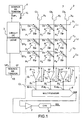
- Column conductors X 1 to X 3 are connected to a read circuit CL comprising, in the example of FIG. figure 1 , an integrator circuit 5, a multiplexer circuit 6, a video amplifier 7 and a converter analog-digital 8.
- the integrator circuit 5 comprises as many amplifiers as conductors in column X 1 to X 3 is, in the example of the figure 1 , three amplifiers G 1 to G 3 . It further comprises an integration capacitor C 1 to C 3 and a switch element I 1 to I 3 for each amplifier G 1 to G 3 .
- Each column conductor X 1 to X 3 is connected to a negative input "-" of an amplifier G 1 to G 3 mounted as an integrator.
- An integration capacitance C 1 to C 3 is connected between the negative input "-" and an output S 1 to S 3 of each amplifier.
- the second input "+” of each amplifier G 1 to G 3 is connected to a potential which, in the example of the figure 1 , is the reference potential Vr.
- Vr the reference potential
- Each amplifier comprises a reset switch element I 1 to I 3, connected in parallel with each integration capacitor C 1 to C 3 .
- the switch elements I 1 to I 3 are, for example, MOS type transistors.
- the integrator circuit 5 thus transforms the charges flowing on the conductors in column X 1 to X 3 in voltages.
- the outputs S 1 to S 3 of the amplifiers G 1 to G 3 are connected to inputs Ent 1 to Ent 3 of the multiplexer circuit 6.
- the multiplexer circuit 6 is for example formed of a parallel input shift register and a serial output be of the charge-coupled type, more commonly called CCD of the English expression "Charged-Coupled Device”. This conventional arrangement makes it possible to deliver "in series” and line after line (from L 1 to L 3 ), at the output of the multiplexer 6, voltages which represent the charges accumulated at the points A of all the photosensitive points P 1 to P 9 . These voltages are called multiplexed signal SM.
- the figures 1 and 2 describe exemplary embodiments of photosensitive devices 1 and 1 'in which the photosensitive points P 1 to P 9 are said to be passive.
- the invention is particularly applicable to photosensitive devices in which the photosensitive spots are said to be active, ie photosensitive spots in which the charges accumulated during an acquisition phase of an image are converted into voltages at the pixels and not outside the matrix in an integrator circuit.
- the figure 3 illustrates such a photosensitive device 1 "having a matrix 2" of two lines L 1 and L 2 by two columns Cl 1 and Cl 2 of points photosensitive P 1 to P 4 .
- the line control circuit 3 has two outputs SY 1 and SY 2 respectively connected to two line conductors Y 1 and Y 2 . It furthermore comprises two outputs S RAZ1 and S RAZ2 respectively connected to two resetting conductors Y RAZ1 , and Y RAZ2 .
- Each photosensitive point P 1 to P 4 comprises a photodiode Dp and three transistors T 1 , T 2 and T 3 .
- the first transistor T 1 of each photosensitive point P 1 to P 4 is connected by its gate G to the resetting conductor Y RAZ1 or Y RAZ2 of the line L 1 or L 2 to which the photosensitive point P 1 to P 4 belongs. considered by its drain D to a voltage source 31 subjecting the drain D to a resetting potential V RAZ and its source S to the cathode of the photodiode Dp belonging to the photosensitive point P 1 to P 4 considered.
- the anodes of all the photodiodes Dp are connected to a common potential, for example the mass.
- the same point A can be defined between the source S of the transistor T 1 and the cathode of the photodiode Dp.
- the transistors T 1 make it possible to return the photosensitive points P 1 to P 4 in their original state, that is to say in the state they had before being exposed to radiation. More particularly, the transistors T 1 make it possible, when a reset pulse is sent by the line control circuit 3 on a resetting conductor Y RAZ1 or Y RAZ2 , to reduce the potential of the point A of all the points. photosensitive P 1 to P 4 of the line L 1 or L 2 considered at the starting potential, in this case the resetting potential V RAZ .
- the reset pulses sent by the line control circuit 3 are for example provided by a voltage source 4 "
- the transistors T 2 make it possible to isolate the points A of the conductors in columns X 1 and X 2 when the transistors T 3 are in the off state, that is to copy (to a constant close) the values of the voltages at the points A on the columns X 1 and X 2 when the transistors T 3 are in the on state.
- the transistors T 3 make it possible to select the line L 1 or L 2 for which it is desired to copy the signals to the points A on the columns X 1 and X 2 .
- the reading of the photosensitive points P 1 to P 4 is also performed line by line.
- the line control circuit successively applies a read pulse to each line conductor Y 1 and Y 2 .
- the voltages at the point A of the photosensitive points P 1 to P 4 belonging to the line L 1 or L 2 which is read are then copied onto the conductors in columns X 1 and X 2 via the transistors T 2 .
- the voltages are copied to a near offset voltage.
- photosensitive devices 1, 1 'and 1 "of Figures 1 to 3 it is considered that the charges are accumulated during an exposure of the photosensitive points P 1 to P 9 by photodiodes Dp.
- these charges can be accumulated by any photosensitive element, for example phototransistors.
- the figure 4 illustrates possible steps for the method of controlling a photosensitive device as for example described with reference to figures 1 , 2 and 3 .
- the control method according to the invention may comprise a first step E 1 , said initialization step.
- the photosensitive points P 1 to P 9 are reset during this step E 1 ; in other words, they are restored to their original state.
- This particular embodiment is shown in Figures 5 and 6 described below.
- photosensitive devices 1 and 1 'passive as represented in figures 1 and 2 it is not the photosensitive points P 1 to P 9 which are reset, but the voltages at the terminals of the integration capacitors C 1 to C 3 via the respective switch elements I 1 to I 3 .
- the value of N may in particular be determined by the user as a function of the exposure time of the photosensitive points P 1 to P 9 and the signal-to-noise ratio of the digital image that he wishes to obtain.
- the value of N can be bounded by the time available between two acquisitions of images. In general, N is greater than 2, but in order not to slow down the reading rate excessively, N will preferably be chosen between 2 and 10.
- the substep E 31 is carried out in the photosensitive devices 1 and 1 'shown in FIGS. figures 1 and 2 by the integrator circuit 5 and in the photosensitive device 1 "shown in FIG. figure 3 , by the transistors T 2 .
- the analog signals representative of the charges are then voltages.
- the signal may optionally undergo a post-processing in a step E 4 and be operated and / or displayed in a step E 5 .
- the post-processing may for example relate to a gain correction for each photosensitive point P 1 to P 9 .
- a gain correction (pixel by pixel) is necessary insofar as the evolution of the ratio between the charges accumulated at a photosensitive point P 1 to P 9 and the integrated voltage for these charges do not correspond to the same coefficient of linearity for all the photosensitive points P 1 to P 9 .
- FIGS. 5 and 6 illustrate, by means of chronograms, two different possibilities of sequencing the processing of the analog signals according to the lines of the matrix 2, 2 'or 2 "For the rest of the description, we consider matrices of photosensitive points organized in Nl lines by Nc columns On the timing charts, a high state is considered as an active state and a low state as a passive state.
- the charges of the photosensitive points belonging to the line whose signals will be processed must be converted before the first processing sub-step E 32 , in accordance with the reading step E 3 described with reference. to the figure 4 .
- the chronograms C 6RAZ , C 6expo , C 61 , C 62 and C 6 N 1 show that, at the end of the exposure period T expo , the first Nc signals are processed for the first time and then the Nc signals from the second line, and so on to the last line where the corresponding signals are also processed a first time.
- the first line, the second line and the following lines are then treated a second time until the last line.
- the steps E 35 of averaging, then the step E 4 of post-processing and the step E 5 of operation and / or display can be realized.
- a new step E 2 acquisition of an image can also be performed.
Description
La présente invention concerne un procédé de commande d'un dispositif photosensible comportant une matrice de points photosensibles, par exemple réalisés par des techniques de dépôt de matériaux semi-conducteurs. Elle s'applique essentiellement, mais non exclusivement, aux dispositifs photosensibles utilisés pour la détection d'images radiologiques.The present invention relates to a method of controlling a photosensitive device comprising a matrix of photosensitive points, for example made by semiconductor material deposition techniques. It applies mainly, but not exclusively, to the photosensitive devices used for the detection of radiological images.
Les technologies utilisant des matériaux semi-conducteurs tels que par exemple :
- le silicium amorphe hydrogéné (aSiH), sur des supports isolants en verre,
- le CMOS sur substrat en silicium cristallin,
- les circuits à couplage de charge (CCD) sur substrat en silicium cristallin,
- hydrogenated amorphous silicon (aSiH), on insulating glass supports,
- CMOS on crystalline silicon substrate,
- charge-coupled circuits (CCD) on a crystalline silicon substrate,
Les points photosensibles qui forment ces matrices comprennent généralement un élément photosensible associé à un élément remplissant une fonction d'interrupteur. Le point photosensible est monté entre un conducteur en ligne et un conducteur en colonne. Selon les besoins, le dispositif photosensible comporte alors une pluralité de points photosensibles agencés en matrice ou en barrette.The photosensitive spots that form these matrices generally comprise a photosensitive element associated with an element that performs a switch function. The photosensitive dot is mounted between an inline conductor and a column conductor. Depending on the needs, the photosensitive device then comprises a plurality of photosensitive points arranged in matrix or bar.
L'élément photosensible est couramment constitué par une diode, montée en série avec l'élément interrupteur. L'élément interrupteur peut être par exemple une diode dite de commutation dont l'état "fermé" ou "passant" correspond à la polarisation qui la met en conduction directe, et dont l'état "ouvert" ou "bloqué" correspond à sa polarisation en inverse. Les deux diodes sont montées avec des sens de conduction opposés, dans une configuration dite "tête-bêche". Une telle disposition est bien connue, notamment de la demande de brevet français
Les conducteurs en colonne sont reliés à un circuit de lecture convertissant les charges accumulées dans les éléments photosensibles en signaux et délivrant ces signaux en sortie. Plus particulièrement, le circuit de lecture peut comporter plusieurs étages. Parmi ces étages, un premier étage peut convertir les charges en signaux analogiques ; un deuxième étage peut amplifier ces signaux ; un troisième étage peut multiplexer les signaux de façon à délivrer "en série" et ligne après ligne en sortie du circuit de lecture, un signal multiplexé comportant les signaux représentatifs des charges accumulées dans les éléments photosensibles ; et un quatrième étage peut convertir le signal multiplexé analogique en signal numérique. Comme tout dispositif électronique, le circuit de lecture introduit un bruit électronique venant s'ajouter aux signaux représentatifs des charges accumulées et limitant le rapport signal sur bruit. En l'occurrence, un bruit est généré à chaque étage du circuit de lecture, et éventuellement plus loin dans la chaîne d'acquisition de l'image. Plus généralement, un bruit est introduit à chaque modification ou transformation d'un signal analogique, jusqu'à ce que ce signal soit converti en signal numérique. Le bruit est particulièrement gênant dans la mesure où les signaux issus du premier étage peuvent avoir une amplitude très faible pour certains modes d'acquisition de l'image, en particulier lorsque le temps d'exposition au rayonnement X est faible. Le rapport signal sur bruit est alors très faible, par exemple proche de l'unité et le signal dit utile, c'est-à-dire représentatif des charges accumulées dans les éléments photosensibles, peut être difficile à extraire du signal global, c'est-à-dire du signal comportant à la fois le signal utile et le bruit.The column conductors are connected to a read circuit converting the accumulated charges in the photosensitive elements into signals and delivering these signals at the output. More particularly, the reading circuit may comprise several stages. Among these stages, a first stage can convert the charges into analog signals; a second stage can amplify these signals; a third stage can multiplex the signals so as to output "in series" and line after line at the output of the read circuit, a multiplexed signal comprising the signals representative of the charges accumulated in the photosensitive elements; and a fourth stage can convert the analog multiplexed signal to a digital signal. Like any electronic device, the reading circuit introduces an electronic noise in addition to the signals representative of the accumulated charges and limiting the signal-to-noise ratio. In this case, a noise is generated at each stage of the read circuit, and possibly further down the image acquisition chain. More generally, a noise is introduced at each modification or transformation of an analog signal, until this signal is converted into a digital signal. The noise is particularly troublesome in that the signals from the first stage can have a very low amplitude for certain image acquisition modes, in particular when the exposure time to X-radiation is low. The signal-to-noise ratio is then very low, for example close to unity and the so-called useful signal, that is to say representative of the charges accumulated in the photosensitive elements, can be difficult to extract from the overall signal, it being that is, the signal comprising both the wanted signal and the noise.
La génération de bruit par la chaîne d'acquisition de l'image peut être limitée par la conception du dispositif photosensible. Cependant, la génération de bruit dépend largement du mode d'utilisation du dispositif photosensible, notamment du temps pendant lequel les points photosensibles sont exposés, de la vitesse de lecture des charges et du gain d'amplification appliqué aux signaux. Ainsi, lors de la conception du dispositif photosensible, un compromis doit être fait entre les différents modes d'utilisation possibles.The noise generation by the image acquisition chain can be limited by the design of the photosensitive device. However, the noise generation depends largely on the mode of use of the photosensitive device, especially the time during which the points photosensitive are exposed, the speed of reading of the charges and the gain of amplification applied to the signals. Thus, during the design of the photosensitive device, a compromise must be made between the various possible modes of use.
Une solution pour diminuer le bruit généré lors du transfert des charges accumulées dans les différents points photosensibles vers un amplificateur de charge est connue de la demande de brevet français publiée sous le numéro
Les demandes de brevets
Un but de l'invention est notamment de pallier tout ou partie des inconvénients précités. A cet effet, l'invention a pour objet procédé de commande d'un dispositif photosensible comprenant une matrice de pixels organisée en lignes et en colonnes, le procédé comprenant une étape d'acquisition d'une image au cours de laquelle chaque pixel est susceptible d'accumuler une charge et une étape de lecture ligne par ligne de cette image, l'étape de lecture comportant :
- une sous-étape de conversion des charges accumulées par chaque pixel de la ligne considérée en signaux analogiques représentatifs de ces charges, et
- une sous-étape de traitement de ces signaux analogiques, ladite sous-étape comprenant une numérisation desdits signaux analogiques, le procédé étant caractérisé en ce que :
- la sous-étape de traitement comprend un multiplexage desdits signaux analogiques de la ligne considérée pour fournir en série un signal multiplexé pour chaque sous-étape de traitement,
- en ce que la sous-étape de traitement est exécutée N fois pour chaque ligne de pixels et pour une même étape d'acquisition, avec N entier supérieur ou égal à deux, et
- en ce que l'étape de lecture comporte une sous-étape de moyennage des N signaux traités pour chaque pixel afin de fournir une seule image numérique par étape d'acquisition.
- a substep of conversion of the charges accumulated by each pixel of the line considered into analog signals representative of these charges, and
- a sub-step of processing these analog signals, said substep comprising digitizing said analog signals, the method being characterized in that:
- the processing sub-step comprises a multiplexing of said analog signals of the line in question to provide a multiplexed signal in series for each sub-step of processing,
- in that the processing sub-step is executed N times for each pixel line and for the same acquisition step, with N being greater than or equal to two, and
- in that the reading step includes a substep of averaging the processed N signals for each pixel to provide a single digital image per acquisition step.
Selon une forme particulière de réalisation, les signaux analogiques sont des tensions.According to a particular embodiment, the analog signals are voltages.
La sous-étape de traitement peut comprendre :
- une conversion des signaux analogiques en signaux numériques ;
- un multiplexage des signaux analogiques ;
- un échantillonnage/blocage des signaux analogiques précédant immédiatement leur multiplexage ;
- une amplification des signaux analogiques ou, le cas échéant, des signaux numériques.
- conversion of the analog signals into digital signals;
- multiplexing the analog signals;
- a sampling / blocking of analog signals immediately preceding their multiplexing;
- amplification of the analog signals or, where appropriate, digital signals.
Selon une forme particulière de réalisation, chaque étape d'acquisition d'une image pour laquelle les points photosensibles sont soumis à une exposition, appelée image utile, est précédée d'une étape d'acquisition d'une image pour laquelle les points photosensibles ne sont pas soumis à une exposition, appelée image d'offset, et d'une étape de lecture de cette image d'offset, l'étape de lecture de l'image d'offset étant identique à l'étape de lecture de l'image utile, l'image utile étant corrigée en fonction de l'image d'offset.According to a particular embodiment, each step of acquisition of an image for which the photosensitive points are subjected to an exposure, called a useful image, is preceded by a step of acquiring an image for which the photosensitive pixels are not subjected to an exposure, called an offset image, and a step of reading this offset image, the step of reading the offset image being identical to the reading step of the useful image, the useful image being corrected according to the offset image.
Dans une première variante, la sous-étape de traitement est répétée N fois pour une même ligne avant de considérer la ligne suivante.In a first variant, the processing sub-step is repeated N times for the same line before considering the next line.
Dans une deuxième variante, la sous-étape de traitement considère chaque ligne successivement avant d'être répétée.In a second variant, the processing sub-step considers each line successively before being repeated.
Selon une première forme de réalisation, les signaux analogiques représentatifs des charges de tous les points photosensibles sont remis à zéro après les N répétitions pour chaque point photosensible de la sous-étape de traitement.According to a first embodiment, the analog signals representative of the charges of all the photosensitive points are reset after the N repetitions for each photosensitive point of the processing sub-step.
Selon une deuxième forme de réalisation, les signaux analogiques représentatifs des charges de tous les points photosensibles de la ligne considérée sont remis à zéro avant de considérer la ligne suivante.According to a second embodiment, the analog signals representative of the charges of all the photosensitive points of the considered line are reset before considering the next line.
L'invention a notamment pour avantage qu'elle permet de diminuer le bruit généré sur la quasi-totalité de la chaîne d'acquisition de l'image. En particulier, le bruit généré dès que les charges sont converties en signaux analogiques peut être réduit.The invention has the particular advantage that it reduces the noise generated on almost the entire image acquisition chain. In particular, the noise generated as soon as the charges are converted into analog signals can be reduced.
L'invention sera mieux comprise et d'autres avantages apparaîtront à la lecture de la description détaillée d'un mode de réalisation donné à titre d'exemple, description faite en regard de dessins annexés qui représentent :
- la
figure 1 , un premier exemple de dispositif photosensible passif auquel peut s'appliquer l'invention ; - la
figure 2 , un deuxième exemple de dispositif photosensible passif auquel peut s'appliquer l'invention ; - la
figure 3 , un exemple de dispositif photosensible actif auquel peut s'appliquer l'invention ; - la
figure 4 , des étapes possibles pour le procédé selon l'invention ; - les
figures 5, 6 et7 , des chronogrammes montrant différentes possibilités d'enchaînement des traitements et des remises à zéro des signaux pour les différentes lignes d'une matrice d'un dispositif photosensible.
- the
figure 1 a first example of a passive photosensitive device to which the invention can be applied; - the
figure 2 a second example of passive photosensitive device to which the invention can be applied; - the
figure 3 an example of an active photosensitive device to which the invention can be applied; - the
figure 4 possible steps for the process according to the invention; - the
Figures 5, 6 and7 , chronograms showing different possibilities of concatenation of processing and resetting of the signals for the different lines of a matrix of a photosensitive device.
La
Dans l'exemple de la
Le dispositif photosensible 1 comporte un circuit de commande ligne 3, dont des sorties SY1, SY2 et SY3 sont reliées respectivement aux conducteurs en ligne Y1, Y2 et Y3. Le circuit de commande ligne 3 dispose de différents éléments, non représentés, tels que par exemple, circuit d'horloge, circuits de commutation, registre à décalage, qui lui permettent de réaliser un adressage séquentiel des conducteurs en ligne Y1 à Y3. Le dispositif photosensible 1 comporte en outre une source de tension 4, délivrant au circuit de commande ligne 3 une tension VP1 servant à définir l'amplitude d'impulsions de polarisation appliquées aux conducteurs en ligne Y1, Y2 et Y3 et une source de tension 13, délivrant au circuit de commande ligne 3 une tension VP2 servant à définir l'amplitude d'impulsions de lecture appliquées aux conducteurs en ligne Y1, Y2 et Y3. Ces deux sources de tensions 4 et 13 peuvent éventuellement être confondues.The
Dans chaque point photosensible P1 à P9, les deux diodes Dp et Dc sont reliées entre elles soit par leur anode, comme représenté à la
Dans la phase d'acquisition d'image ou de prise d'image, c'est-à-dire pendant la phase d'exposition de la matrice 2 à un signal lumineux dit "utile", les deux diodes Dp et Dc de chaque point photosensible P1 à P9 sont polarisées en inverse. Dans cet état, elles constituent chacune une capacité. Il est à noter que généralement les deux diodes Dp et Dc sont conçues pour que la capacité présentée par la photodiode Dp soit la plus forte, de l'ordre par exemple de 50 fois.In the image acquisition or imaging phase, that is to say during the exposure phase of the
Lors de l'acquisition d'une image, des charges sont engendrées dans la photodiode Dp par l'exposition du point photosensible P1 à P9 auquel elle appartient. Ces charges, dont la quantité est fonction de l'intensité d'exposition, s'accumulent en un point A sur le noeud formé au point de jonction des deux diodes Dp et Dc. La lecture des points photosensibles P1 à P9 s'effectue ligne par ligne, simultanément pour tous les points photosensibles reliés à un même conducteur en ligne Y1 à Y3. A cet effet, le circuit de commande ligne 3 applique à chaque conducteur en ligne Y1 à Y3 adressé, une impulsion dite de lecture d'amplitude VP2. Les conducteurs en ligne qui ne sont pas adressés sont maintenus à un potentiel de référence Vr ou potentiel de repos. Ce potentiel de référence Vr est par exemple la masse. Il peut être le même potentiel que celui qui est appliqué aux conducteurs en colonne X1 à X3.During the acquisition of an image, charges are generated in the photodiode Dp by the exposure of the photosensitive point P 1 to P 9 to which it belongs. These charges, whose quantity is a function of the intensity of exposure, accumulate at a point A on the node formed at the junction point of the two diodes Dp and Dc. The photosensitive points P 1 to P 9 are read line by line, simultaneously for all the photosensitive points connected to the same line conductor Y 1 to Y 3 . For this purpose, the
L'éventuelle accumulation de charges au point A d'un point photosensible P1 à P9 entraîne en ce point une diminution de la tension, c'est-à-dire une diminution de la tension de polarisation inverse de la photodiode Dp. Avec certains modes de fonctionnement, l'application de l'impulsion de lecture à un conducteur en ligne Y1 à Y3 a pour effet de restituer au potentiel du point A de tous les points photosensibles reliés à ce conducteur en ligne, le niveau de polarisation qu'il possédait avant l'exposition au signal lumineux utile. Il en résulte une circulation dans chacun des conducteurs en colonne X1 à X3 d'un courant proportionnel aux charges accumulées au point A correspondant.The possible accumulation of charges at the point A of a photosensitive point P 1 to P 9 causes at this point a decrease in the voltage, that is to say a decrease in the reverse bias voltage of the photodiode Dp. With certain operating modes, the application of the read pulse to an on-line conductor Y 1 to Y 3 has the effect of restoring to the potential of point A of all the photosensitive points connected to this line conductor, the level of polarization it possessed before exposure to the useful light signal. This results in a circulation in each of the conductors in column X 1 to X 3 of a current proportional to the accumulated charges at the corresponding point A.
Les conducteurs en colonne X1 à X3 sont reliés à un circuit de lecture CL comprenant, dans l'exemple de la
Les sorties S1 à S3 des amplificateurs G1 à G3 sont reliées à des entrées Ent1 à Ent3 du circuit multiplexeur 6. Le circuit multiplexeur 6 est par exemple formé d'un registre à décalage à entrées parallèles et sortie série pouvant être du type à couplage de charges, plus communément appelé C.C.D. de l'expression anglo-saxonne "Charged-Coupled Device". Cette disposition classique permet de délivrer "en série" et ligne après ligne (de L1 à L3), en sortie du multiplexeur 6, des tensions qui représentent les charges accumulées aux points A de tous les points photosensibles P1 à P9. Ces tensions sont appelées signal multiplexé SM.The outputs S 1 to S 3 of the amplifiers G 1 to G 3 are connected to inputs Ent 1 to Ent 3 of the
Le signal multiplexé SM peut ensuite être amplifié par l'amplificateur vidéo 7 et converti en un signal numérique SN par un convertisseur analogique-numérique 8.The multiplexed signal SM can then be amplified by the video amplifier 7 and converted into a digital signal SN by an analog-to-
Il est à noter qu'il est connu aussi, pour remplir la fonction d'interrupteur qui, dans l'exemple de la
La
Dans le schéma montré à la
Pour mieux comprendre le fonctionnement général des dispositifs représentés aux
Les
La
Les transistors T1 permettent de remettre les points photosensibles P1 à P4 dans leur état d'origine, c'est-à-dire dans l'état qu'ils avaient avant d'être exposés à un rayonnement. Plus particulièrement, les transistors T1 permettent, lorsqu'une impulsion de remise à zéro est envoyée par le circuit de commande ligne 3 sur un conducteur de remise à zéro YRAZ1 ou YRAZ2, de ramener le potentiel du point A de tous les points photosensibles P1 à P4 de la ligne L1 ou L2 considérée au potentiel de départ, en l'occurrence le potentiel de remise à zéro VRAZ. Les impulsions de remise à zéro envoyées par le circuit de commande ligne 3 sont par exemple fournies par une source de tension 4". Les transistors T2 permettent soit d'isoler les points A des conducteurs en colonne X1 et X2 lorsque les transistors T3 sont à l'état bloqué, soit de copier (à une constante près) les valeurs des tensions aux points A sur les colonnes X1 et X2 lorsque les transistors T3 sont à l'état passant. Les transistors T3 permettent de sélectionner la ligne L1 ou L2 pour laquelle on souhaite copier les signaux aux points A sur les colonnes X1 et X2.The transistors T 1 make it possible to return the photosensitive points P 1 to P 4 in their original state, that is to say in the state they had before being exposed to radiation. More particularly, the transistors T 1 make it possible, when a reset pulse is sent by the
La lecture des points photosensibles P1 à P4 s'effectue également ligne par ligne. Le circuit de commande ligne applique successivement une impulsion de lecture à chaque conducteur en ligne Y1 et Y2. Les tensions au point A des points photosensibles P1 à P4 appartenant à la ligne L1 ou L2 qui est lue sont alors recopiées sur les conducteurs en colonne X1 et X2 par l'intermédiaire des transistors T2. Les tensions sont recopiées à une tension de décalage près.The reading of the photosensitive points P 1 to P 4 is also performed line by line. The line control circuit successively applies a read pulse to each line conductor Y 1 and Y 2 . The voltages at the point A of the photosensitive points P 1 to P 4 belonging to the line L 1 or L 2 which is read are then copied onto the conductors in columns X 1 and X 2 via the transistors T 2 . The voltages are copied to a near offset voltage.
Contrairement aux dispositifs photosensibles 1 et 1' des
La
Dans les dispositifs photosensibles 1, 1' et 1 " des
La
La sous-étape E31 est réalisée dans les dispositifs photosensibles 1 et 1' représentés aux
La sous-étape E32 peut comporter un multiplexage 322 des signaux analogiques afin de fournir en série, pour chaque sous-étape E32 de traitement, un signal multiplexé SM. Le multiplexage 322 est par exemple réalisé par le multiplexeur 6 représenté aux
Selon l'invention, la sous-étape E32 de traitement est répétée N fois après chaque étape E2 d'acquisition d'une image et ce, pour chaque ligne de points photosensibles. Pour chaque étape E2, on obtient donc N signaux multiplexés SM par ligne. Selon une forme particulière de réalisation, la répétition de la sous-étape E32 est obtenue par l'intermédiaire d'un compteur de lectures dont la valeur est notée n. Selon cette forme particulière de réalisation, durant l'étape E1 d'initialisation, la valeur n du compteur de lectures est mise à la valeur un. A l'issue de la sous-étape E32 de traitement, on peut déterminer dans une sous-étape E33 si la valeur n du compteur est égale à la valeur N. Si tel n'est pas le cas, on peut incrémenter d'une unité la valeur n du compteur dans une sous-étape E34 et réitérer la sous-étape E32 dans son intégralité. Si la valeur n du compteur est égale à la valeur N, on moyenne alors dans une sous-étape E35 les N signaux traités obtenus pour chaque point photosensible P1 à P9. Lors d'un traitement ligne par ligne, les N signaux traités obtenus proviennent de chaque point photosensible d'une même ligne, par exemple P1 à P3. L'étape E3 est répétée pour chaque ligne (pixels P4 à P6, puis pixels P7 à P9). Le moyennage est par exemple un moyennage arithmétique ou quadratique. Il peut également être pondéré en fonction de la valeur n du compteur de lectures ou d'une amplitude de certains signaux. Il est également possible d'éliminer des valeurs aberrantes de signaux, par exemple situées en dehors de fourchettes prédéterminées. Le moyennage peut notamment être effectué sur les N signaux multiplexés et numérisés. Le signal obtenu par la sous-étape E35 de moyennage peut alors être exploité par le reste de la chaîne d'acquisition d'une image de la même façon que s'il s'agissait d'un signal issu d'une seule sous-étape E32 de traitement.According to the invention, the processing sub-step E 32 is repeated N times after each image acquisition step E 2 and for each line of photosensitive points. For each step E 2 , N multiplexed signals SM per line are thus obtained. According to a particular embodiment, the repetition of the substep E 32 is obtained by means of a read counter whose value is denoted n. According to this particular embodiment, during the initialization step E 1 , the value n of the read counter is set to one. At the end of the processing sub-step E 32 , it can be determined in a substep E 33 whether the value n of the counter is equal to the value N. If this is not the case, it is possible to increment a unit the value n of the counter in a substep E 34 and reiterate substep E 32 in its entirety. If the value n of the counter is equal to the value N, then the processed N signals obtained for each photosensitive point P 1 to P 9 are averaged in a substep E 35 . During line-by-line processing, the N processed signals obtained come from each photosensitive point of the same line, for example P 1 to P 3 . Step E 3 is repeated for each line (pixels P 4 to P 6 , then pixels P 7 to P 9 ). The averaging is for example an arithmetic or quadratic averaging. It can also be weighted according to the value n of the reading counter or an amplitude of certain signals. It is also possible to eliminate outliers of signals, for example located outside predetermined ranges. The averaging can in particular be carried out on the N multiplexed and digitized signals. The signal obtained by the substep E 35 of averaging can then be exploited by the rest of the acquisition chain of an image in the same way as if it were a signal coming from a single slot. step E 32 of treatment.
L'invention permet de réduire les bruits électroniques introduits dans la sous-étape E32 de traitement des signaux analogiques dans la mesure où ces bruits sont au moins partiellement décorrélés les uns des autres entre deux traitements et s'annulent donc partiellement. Plus particulièrement, pour des bruits complètement décorrélés, le bruit global pour N sous-étapes E32 de traitement est divisé par la racine carrée de N ![]()
![]()
A l'issue de l'étape E3 de lecture, le signal peut éventuellement subir un post-traitement dans une étape E4 et être exploité et/ou affiché dans une étape E5. Le post-traitement peut par exemple concerner une correction de gain pour chaque point photosensible P1 à P9. Une correction de gain (pixel à pixel) est nécessaire dans la mesure où l'évolution du rapport entre les charges accumulées en un point photosensible P1 à P9 et la tension intégrée pour ces charges ne correspond pas au même coefficient de linéarité pour tous les points photosensibles P1 à P9.At the end of the reading step E 3 , the signal may optionally undergo a post-processing in a step E 4 and be operated and / or displayed in a step E 5 . The post-processing may for example relate to a gain correction for each photosensitive point P 1 to P 9 . A gain correction (pixel by pixel) is necessary insofar as the evolution of the ratio between the charges accumulated at a photosensitive point P 1 to P 9 and the integrated voltage for these charges do not correspond to the same coefficient of linearity for all the photosensitive points P 1 to P 9 .
Selon une forme particulière de réalisation, chaque étape E2 d'acquisition d'une image utile, c'est-à-dire d'une image pour laquelle les points photosensibles P1 à P9 ont été soumis à une exposition, est précédée d'une étape d'acquisition d'une image d'offset, c'est-à-dire d'une image pour laquelle les points photosensibles P1 à P9 n'ont pas été soumis à une exposition, et d'une étape de lecture de cette image d'offset. Lors de l'étape E4 de post-traitement, il est alors possible de corriger l'image utile en fonction de l'image d'offset. Une correction d'offset est généralement nécessaire dans la mesure où les composants semi-conducteurs utilisés dans les dispositifs photosensibles 1, 1' et 1 ", en particulier les photodiodes Dp, les diodes de commutation Dc et les transistors T1, T2 et T3 ne sont pas tous strictement identiques. L'image utile englobant l'image d'offset, la correction de l'image utile en fonction de l'image d'offset peut être effectuée par une soustraction pixel par pixel entre l'image utile et l'image d'offset. Dans le cas où il n'y a pas de remise à zéro de l'étage de conversion charges/tension, la correction d'offset consiste en un double échantillonnage corrélé.According to a particular embodiment, each step E 2 of acquisition of a useful image, that is to say of an image for which the photosensitive points P 1 to P 9 have been subjected to an exposure, is preceded a step of acquiring an offset image, that is to say an image for which the photosensitive points P 1 to P 9 have not been subjected to an exposure, and a reading step of this offset image. During the post-processing step E 4 , it is then possible to correct the useful image as a function of the offset image. An offset correction is generally necessary insofar as the semiconductor components used in the
Toujours selon une forme particulière de réalisation, l'étape de lecture de l'image d'offset est identique à l'étape E3 de lecture de l'image utile. En d'autres termes, les signaux analogiques représentatifs des charges accumulées dans les points photosensibles P1 à P9 en l'absence d'exposition et appelés signaux d'offset sont traités N fois puis moyennés pixel par pixel afin de diminuer le bruit généré par la sous-étape E32 de traitement de la même manière que pour les signaux utiles.Still according to a particular embodiment, the step of reading the offset image is identical to the step E 3 for reading the useful image. In other words, the analog signals representative of the charges accumulated in the photosensitive points P 1 to P 9 in the absence of exposure and called offset signals are processed N times and averaged pixel by pixel in order to reduce the noise generated. by the processing sub-step E 32 in the same way as for the useful signals.
Selon une forme particulière de réalisation, le procédé de commande selon l'invention comporte plusieurs enchaînements des sous-étapes E32 de traitement et E35 de moyennage, les sous-étapes E32 de traitement pouvant différer selon l'enchaînement. A titre d'exemple, une première sous-étape E32 de traitement peut comporter un échantillonnage/blocage 321 et un multiplexage 322 des signaux analogiques et une deuxième sous-étape E32 peut comporter une amplification 323 et une numérisation 324 du signal multiplexé SM, chaque sous-étape E32 étant répétée N fois avant que les N signaux qui en sont issus soient respectivement moyennés dans une première et dans une deuxième sous-étape de moyennage E35.According to one particular embodiment, the control method according to the invention comprises several sequences of the processing sub-steps E 32 and averaging E 35 , the processing sub-steps E 32 being able to differ according to the sequence. By way of example, a first processing sub-step E 32 may comprise a sampling / blocking 321 and a multiplexing 322 of the analog signals and a second substep E 32 may include an
Les
La
- chaque période Texpo est précédée d'une période TRAZ ;
- à l'issue de la période Texpo, les Nc signaux de la première ligne sont traités trois fois ;
- après le dernier traitement des signaux de la première ligne, les Nc signaux de la deuxième ligne sont à leur tour traités trois fois ;
- et ainsi de suite jusqu'à la dernière ligne où les signaux correspondants sont traités trois fois.
- each period T expo is preceded by a period T RAZ ;
- at the end of the period T expo , the Nc signals of the first line are processed three times;
- after the last signal processing of the first line, the Nc signals of the second line are in turn processed three times;
- and so on until the last line where the corresponding signals are processed three times.
La sous-étape E35 et les étapes E4 et E5 peuvent ensuite être réalisées. Une nouvelle étape E2 d'acquisition d'une image peut être effectuée dès la fin de la dernière itération de la sous-étape E32 de traitement de la dernière ligne.Sub-step E 35 and steps E 4 and E 5 can then be performed. A new step E 2 acquisition of an image can be performed at the end of the last iteration of the substep E 32 processing of the last line.
Bien entendu, pour un dispositif photosensible passif, les charges des points photosensibles appartenant à la ligne dont les signaux vont être traités doivent être converties avant la première sous-étape E32 de traitement, conformément à l'étape E3 de lecture décrite en référence à la
La
Selon une forme particulière de réalisation, représentée aux
La
L'invention permet de réduire le bruit généré par la chaîne d'acquisition de l'image de façon simple et économique, aucune modification matérielle de la chaîne d'acquisition de l'image n'étant nécessaire. Le nombre N de traitements effectué par point photosensible peut facilement être adapté en fonction du rapport signal sur bruit souhaité et des ressources matérielles de la chaîne d'acquisition de l'image.The invention makes it possible to reduce the noise generated by the acquisition chain of the image simply and economically, no hardware modification of the image acquisition chain being necessary. The number N of treatments performed by photosensitive dot can easily be adapted according to the desired signal-to-noise ratio and hardware resources of the image acquisition chain.
Claims (10)
- A method for controlling a photosensitive device (1, 1', 1") comprising a matrix (2, 2', 2") of pixels (P1 to P9) organised in rows (L1 to L3) and columns (Cl1 to Cl3), the method comprising
a step (E2) of acquiring an image in the course of which each pixel (P1 to P9) is able to accumulate a charge and
a step (E3) of reading this image row by row, the reading step (E3) comprising:a sub-step (E31) of converting the charges accumulated by each pixel (P1 to P9) of the row being considered into analogue signals representative of these charges, anda sub-step (E32) of processing these analogue signals, said sub-step comprising digitisation (324) of said analogue signals,the method being characterised in that:the processing sub-step (E32) comprises multiplexing (322) of said analogue signals of the row being considered so as to provide in series a multiplexed signal for each processing sub-step (E32),in that the processing sub-step (E32) is executed N times for each row of pixels (P1 to P9) and for each acquisition step (E2), with N an integer greater than or equal to two, andin that the reading step (E3) comprises a sub-step (E35) of averaging the N signals processed for each pixel (P1 to P9) so as to provide a single digital image for each acquisition step (E2). - The method according to Claim 1, characterised in that the analogue signals are voltages.
- The method according to either of Claims 1 or 2, characterised in that the processing sub-step (E32) comprises a conversion (324) of the analogue signals (SM) into digital signals (SN).
- The method according to any of the preceding claims, characterised in that the processing sub-step (E32) comprises sampling/blocking (321) of the analogue signals immediately preceding their multiplexing (322).
- The method according to any of the preceding claims, characterised in that the processing sub-step (E32) comprises amplification (323) of the analogue signals or, if appropriate, of the digital signals (SN).
- The method according to any of the preceding claims, characterised in that each step (E2) of acquiring an image for which the pixels (P1 to P9) are subjected to exposure, called a useful image, is preceded by a step (E2) of acquiring an image for which the pixels (P1 to P9) are not subjected to exposure, called an offset image, and by a step (E3) of reading this offset image, the step (E3) of reading the offset image being identical to the step (E3) of reading the useful image, the useful image being corrected as a function of the offset image.
- The method according to any of the preceding claims, characterised in that the processing sub-step (E32) is executed N times for each row before considering the next row.
- The method according to any of Claims 1 to 6, characterised in that the processing sub-step (E32) considers each row in succession before being repeated.
- The method according to any of the preceding claims, characterised in that the analogue signals representative of the charges of all of the pixels are re-set to zero after the N executions for each pixel (P1 to P9) of the processing sub-step (E32).
- The method according to Claim 7, characterised in that the analogue signals representative of the charges of all of the pixels (P1 to P9) of the row being considered are re-set to zero before considering the next row.
Applications Claiming Priority (2)
| Application Number | Priority Date | Filing Date | Title |
|---|---|---|---|
| FR0904847A FR2951311A1 (en) | 2009-10-09 | 2009-10-09 | METHOD FOR CONTROLLING A PHOTOSENSITIVE DEVICE |
| PCT/EP2010/006187 WO2011042204A2 (en) | 2009-10-09 | 2010-10-11 | Method for controlling a light-sensitive device |
Publications (2)
| Publication Number | Publication Date |
|---|---|
| EP2486724A2 EP2486724A2 (en) | 2012-08-15 |
| EP2486724B1 true EP2486724B1 (en) | 2015-09-16 |
Family
ID=42111167
Family Applications (1)
| Application Number | Title | Priority Date | Filing Date |
|---|---|---|---|
| EP10810960.4A Active EP2486724B1 (en) | 2009-10-09 | 2010-10-11 | Method for reducing noise in the image signal of an image sensor |
Country Status (7)
| Country | Link |
|---|---|
| US (1) | US8994853B2 (en) |
| EP (1) | EP2486724B1 (en) |
| JP (1) | JP6177525B2 (en) |
| CN (1) | CN102763403B (en) |
| CA (1) | CA2777080A1 (en) |
| FR (1) | FR2951311A1 (en) |
| WO (1) | WO2011042204A2 (en) |
Families Citing this family (1)
| Publication number | Priority date | Publication date | Assignee | Title |
|---|---|---|---|---|
| US9752929B2 (en) * | 2014-05-08 | 2017-09-05 | Pinnacle Imaging Corporation | Light-detecting device and method for converting optical radiation on switched conductivity diodes |
Family Cites Families (19)
| Publication number | Priority date | Publication date | Assignee | Title |
|---|---|---|---|---|
| JPS6386976A (en) | 1986-09-30 | 1988-04-18 | Nec Corp | Noise eliminating circuit |
| FR2605166B1 (en) | 1986-10-09 | 1989-02-10 | Thomson Csf | SOLID PHOTOSENSITIVE DEVICE, READING METHOD, AND MANUFACTURING METHOD |
| FR2625593B1 (en) | 1988-01-05 | 1990-05-04 | Thomson Csf | LOW NOISE READING METHOD AND CIRCUIT FOR LINE TRANSFER PHOTOSENSITIVE MATRIX |
| US5276508A (en) * | 1992-11-05 | 1994-01-04 | Eastman Kodak Company | Analog signal processor for electronic imaging system providing highly accurate reproduction of images |
| US5661521A (en) * | 1995-06-05 | 1997-08-26 | Eastman Kodak Company | Smear correction of CCD imager using active pixels |
| US5946033A (en) * | 1996-05-28 | 1999-08-31 | Gatan, Inc. | Method and apparatus for multiple read-out speeds for a CTD |
| FR2760585B1 (en) | 1997-03-07 | 1999-05-28 | Thomson Tubes Electroniques | METHOD FOR CONTROLLING A LOW RETENTION PHOTOSENSITIVE DEVICE, AND PHOTOSENSITIVE DEVICE IMPLEMENTING THE METHOD |
| FR2772161B1 (en) | 1997-12-09 | 2000-02-25 | Trixell Sas | CORRECTION METHOD FOR THE NOISE LEVEL OF A DIGITAL IMAGE DETECTOR |
| US7054474B1 (en) * | 2001-07-25 | 2006-05-30 | 3D Sharp, Inc. | Image noise reduction |
| US7068319B2 (en) * | 2002-02-01 | 2006-06-27 | Micron Technology, Inc. | CMOS image sensor with a low-power architecture |
| US6904126B2 (en) * | 2002-06-19 | 2005-06-07 | Canon Kabushiki Kaisha | Radiological imaging apparatus and method |
| CN101305397B (en) | 2005-10-12 | 2012-09-19 | 有源光学有限公司 | Method for forming image based on a plurality of image frames, image processing system and digital camera |
| WO2007099620A1 (en) * | 2006-03-01 | 2007-09-07 | Fujitsu Limited | Semiconductor integrated circuit |
| JP2008011284A (en) | 2006-06-30 | 2008-01-17 | Fujitsu Ltd | Image processing circuit, imaging circuit and electronic apparatus |
| JP2008124527A (en) | 2006-11-08 | 2008-05-29 | Sony Corp | Solid-state imaging device and imaging apparatus |
| US20080122962A1 (en) * | 2006-11-29 | 2008-05-29 | Omnivision Technologies, Inc. | Image sensors with output noise reduction mechanisms |
| KR101448917B1 (en) | 2007-09-11 | 2014-10-13 | 삼성전자주식회사 | Apparatus and Method for converting Analogue to Digital using pseudo multiple sampling |
| JP4553949B2 (en) | 2008-03-07 | 2010-09-29 | 大阪瓦斯株式会社 | grill |
| JP5347341B2 (en) | 2008-06-06 | 2013-11-20 | ソニー株式会社 | Solid-state imaging device, imaging device, electronic device, AD conversion device, AD conversion method |
-
2009
- 2009-10-09 FR FR0904847A patent/FR2951311A1/en active Pending
-
2010
- 2010-10-11 EP EP10810960.4A patent/EP2486724B1/en active Active
- 2010-10-11 CA CA2777080A patent/CA2777080A1/en not_active Abandoned
- 2010-10-11 US US13/501,055 patent/US8994853B2/en active Active
- 2010-10-11 CN CN201080054461.7A patent/CN102763403B/en active Active
- 2010-10-11 WO PCT/EP2010/006187 patent/WO2011042204A2/en active Application Filing
- 2010-10-11 JP JP2012532495A patent/JP6177525B2/en active Active
Also Published As
| Publication number | Publication date |
|---|---|
| JP6177525B2 (en) | 2017-08-09 |
| WO2011042204A2 (en) | 2011-04-14 |
| WO2011042204A3 (en) | 2011-06-16 |
| US20120314112A1 (en) | 2012-12-13 |
| FR2951311A1 (en) | 2011-04-15 |
| CN102763403B (en) | 2015-08-19 |
| CA2777080A1 (en) | 2011-04-14 |
| CN102763403A (en) | 2012-10-31 |
| JP2013507805A (en) | 2013-03-04 |
| EP2486724A2 (en) | 2012-08-15 |
| US8994853B2 (en) | 2015-03-31 |
Similar Documents
| Publication | Publication Date | Title |
|---|---|---|
| EP2567541B1 (en) | Image sensor having a sampler array | |
| EP2567540B1 (en) | Swipe linear image sensor with analog and digital summation and corresponding method | |
| EP1265291A1 (en) | CMOS image sensor and method for driving a CMOS image sensor with increased dynamic range | |
| EP3122035B1 (en) | Active pixel image sensor with operation in global shutter mode, reset noise subtraction and non-destructive reading | |
| FR2961019A1 (en) | LINEAR IMAGE SENSOR IN CMOS TECHNOLOGY | |
| FR2973162A1 (en) | VERY HIGH DYNAMIC IMAGE SENSOR | |
| EP2064868A1 (en) | Cmos linear image sensor operating by charge transfer | |
| EP2486724B1 (en) | Method for reducing noise in the image signal of an image sensor | |
| EP1673932B1 (en) | Control method for a photosensitive device | |
| EP1290869A1 (en) | Method for converting an analog signal into a digital signal and electromagnetic radiation sensor using same | |
| EP2394424B1 (en) | Method of correcting images obtained from an array of photosensitive point | |
| CA2449939C (en) | Method for controlling a photosensitive device | |
| WO2014096433A1 (en) | Method for reading an imaging device | |
| WO2017125316A1 (en) | Control method for an active pixel image sensor | |
| EP3026890B1 (en) | Control of the integration time in a photosensitive device | |
| FR3131421A1 (en) | Image sensor and method for controlling such a sensor | |
| EP3005684A1 (en) | Cmos sensor with standard photosites | |
| FR3119707A1 (en) | Digital detector with digital integration of charges | |
| WO2020049460A1 (en) | Imaging device with a high acquisition speed and an extended dynamic range | |
| EP2664132A1 (en) | Cmos linear image sensor with motion-blur compensation |
Legal Events
| Date | Code | Title | Description |
|---|---|---|---|
| PUAI | Public reference made under article 153(3) epc to a published international application that has entered the european phase |
Free format text: ORIGINAL CODE: 0009012 |
|
| 17P | Request for examination filed |
Effective date: 20120416 |
|
| AK | Designated contracting states |
Kind code of ref document: A2 Designated state(s): AL AT BE BG CH CY CZ DE DK EE ES FI FR GB GR HR HU IE IS IT LI LT LU LV MC MK MT NL NO PL PT RO RS SE SI SK SM TR |
|
| DAX | Request for extension of the european patent (deleted) | ||
| 17Q | First examination report despatched |
Effective date: 20130206 |
|
| REG | Reference to a national code |
Ref country code: DE Ref legal event code: R079 Ref document number: 602010027619 Country of ref document: DE Free format text: PREVIOUS MAIN CLASS: H04N0005335000 Ipc: H04N0005210000 |
|
| GRAP | Despatch of communication of intention to grant a patent |
Free format text: ORIGINAL CODE: EPIDOSNIGR1 |
|
| RIC1 | Information provided on ipc code assigned before grant |
Ipc: H04N 5/357 20110101ALI20150326BHEP Ipc: H04N 5/335 20110101ALI20150326BHEP Ipc: H04N 5/217 20110101ALI20150326BHEP Ipc: H04N 5/21 20060101AFI20150326BHEP |
|
| INTG | Intention to grant announced |
Effective date: 20150417 |
|
| GRAS | Grant fee paid |
Free format text: ORIGINAL CODE: EPIDOSNIGR3 |
|
| GRAA | (expected) grant |
Free format text: ORIGINAL CODE: 0009210 |
|
| AK | Designated contracting states |
Kind code of ref document: B1 Designated state(s): AL AT BE BG CH CY CZ DE DK EE ES FI FR GB GR HR HU IE IS IT LI LT LU LV MC MK MT NL NO PL PT RO RS SE SI SK SM TR |
|
| REG | Reference to a national code |
Ref country code: GB Ref legal event code: FG4D Free format text: NOT ENGLISH |
|
| REG | Reference to a national code |
Ref country code: CH Ref legal event code: EP |
|
| REG | Reference to a national code |
Ref country code: IE Ref legal event code: FG4D Free format text: LANGUAGE OF EP DOCUMENT: FRENCH |
|
| REG | Reference to a national code |
Ref country code: AT Ref legal event code: REF Ref document number: 750587 Country of ref document: AT Kind code of ref document: T Effective date: 20151015 |
|
| REG | Reference to a national code |
Ref country code: DE Ref legal event code: R096 Ref document number: 602010027619 Country of ref document: DE |
|
| PG25 | Lapsed in a contracting state [announced via postgrant information from national office to epo] |
Ref country code: GR Free format text: LAPSE BECAUSE OF FAILURE TO SUBMIT A TRANSLATION OF THE DESCRIPTION OR TO PAY THE FEE WITHIN THE PRESCRIBED TIME-LIMIT Effective date: 20151217 Ref country code: LT Free format text: LAPSE BECAUSE OF FAILURE TO SUBMIT A TRANSLATION OF THE DESCRIPTION OR TO PAY THE FEE WITHIN THE PRESCRIBED TIME-LIMIT Effective date: 20150916 Ref country code: NO Free format text: LAPSE BECAUSE OF FAILURE TO SUBMIT A TRANSLATION OF THE DESCRIPTION OR TO PAY THE FEE WITHIN THE PRESCRIBED TIME-LIMIT Effective date: 20151216 Ref country code: FI Free format text: LAPSE BECAUSE OF FAILURE TO SUBMIT A TRANSLATION OF THE DESCRIPTION OR TO PAY THE FEE WITHIN THE PRESCRIBED TIME-LIMIT Effective date: 20150916 Ref country code: LV Free format text: LAPSE BECAUSE OF FAILURE TO SUBMIT A TRANSLATION OF THE DESCRIPTION OR TO PAY THE FEE WITHIN THE PRESCRIBED TIME-LIMIT Effective date: 20150916 |
|
| REG | Reference to a national code |
Ref country code: LT Ref legal event code: MG4D Ref country code: NL Ref legal event code: FP |
|
| REG | Reference to a national code |
Ref country code: AT Ref legal event code: MK05 Ref document number: 750587 Country of ref document: AT Kind code of ref document: T Effective date: 20150916 |
|
| PG25 | Lapsed in a contracting state [announced via postgrant information from national office to epo] |
Ref country code: HR Free format text: LAPSE BECAUSE OF FAILURE TO SUBMIT A TRANSLATION OF THE DESCRIPTION OR TO PAY THE FEE WITHIN THE PRESCRIBED TIME-LIMIT Effective date: 20150916 Ref country code: RS Free format text: LAPSE BECAUSE OF FAILURE TO SUBMIT A TRANSLATION OF THE DESCRIPTION OR TO PAY THE FEE WITHIN THE PRESCRIBED TIME-LIMIT Effective date: 20150916 Ref country code: SE Free format text: LAPSE BECAUSE OF FAILURE TO SUBMIT A TRANSLATION OF THE DESCRIPTION OR TO PAY THE FEE WITHIN THE PRESCRIBED TIME-LIMIT Effective date: 20150916 |
|
| PG25 | Lapsed in a contracting state [announced via postgrant information from national office to epo] |
Ref country code: CZ Free format text: LAPSE BECAUSE OF FAILURE TO SUBMIT A TRANSLATION OF THE DESCRIPTION OR TO PAY THE FEE WITHIN THE PRESCRIBED TIME-LIMIT Effective date: 20150916 Ref country code: IS Free format text: LAPSE BECAUSE OF FAILURE TO SUBMIT A TRANSLATION OF THE DESCRIPTION OR TO PAY THE FEE WITHIN THE PRESCRIBED TIME-LIMIT Effective date: 20160116 Ref country code: SK Free format text: LAPSE BECAUSE OF FAILURE TO SUBMIT A TRANSLATION OF THE DESCRIPTION OR TO PAY THE FEE WITHIN THE PRESCRIBED TIME-LIMIT Effective date: 20150916 Ref country code: ES Free format text: LAPSE BECAUSE OF FAILURE TO SUBMIT A TRANSLATION OF THE DESCRIPTION OR TO PAY THE FEE WITHIN THE PRESCRIBED TIME-LIMIT Effective date: 20150916 Ref country code: EE Free format text: LAPSE BECAUSE OF FAILURE TO SUBMIT A TRANSLATION OF THE DESCRIPTION OR TO PAY THE FEE WITHIN THE PRESCRIBED TIME-LIMIT Effective date: 20150916 Ref country code: IT Free format text: LAPSE BECAUSE OF FAILURE TO SUBMIT A TRANSLATION OF THE DESCRIPTION OR TO PAY THE FEE WITHIN THE PRESCRIBED TIME-LIMIT Effective date: 20150916 |
|
| REG | Reference to a national code |
Ref country code: DE Ref legal event code: R119 Ref document number: 602010027619 Country of ref document: DE |
|
| PG25 | Lapsed in a contracting state [announced via postgrant information from national office to epo] |
Ref country code: PL Free format text: LAPSE BECAUSE OF FAILURE TO SUBMIT A TRANSLATION OF THE DESCRIPTION OR TO PAY THE FEE WITHIN THE PRESCRIBED TIME-LIMIT Effective date: 20150916 Ref country code: PT Free format text: LAPSE BECAUSE OF FAILURE TO SUBMIT A TRANSLATION OF THE DESCRIPTION OR TO PAY THE FEE WITHIN THE PRESCRIBED TIME-LIMIT Effective date: 20160118 Ref country code: RO Free format text: LAPSE BECAUSE OF FAILURE TO SUBMIT A TRANSLATION OF THE DESCRIPTION OR TO PAY THE FEE WITHIN THE PRESCRIBED TIME-LIMIT Effective date: 20150916 Ref country code: AT Free format text: LAPSE BECAUSE OF FAILURE TO SUBMIT A TRANSLATION OF THE DESCRIPTION OR TO PAY THE FEE WITHIN THE PRESCRIBED TIME-LIMIT Effective date: 20150916 |
|
| REG | Reference to a national code |
Ref country code: CH Ref legal event code: PL |
|
| PG25 | Lapsed in a contracting state [announced via postgrant information from national office to epo] |
Ref country code: MC Free format text: LAPSE BECAUSE OF FAILURE TO SUBMIT A TRANSLATION OF THE DESCRIPTION OR TO PAY THE FEE WITHIN THE PRESCRIBED TIME-LIMIT Effective date: 20150916 |
|
| PLBE | No opposition filed within time limit |
Free format text: ORIGINAL CODE: 0009261 |
|
| STAA | Information on the status of an ep patent application or granted ep patent |
Free format text: STATUS: NO OPPOSITION FILED WITHIN TIME LIMIT |
|
| REG | Reference to a national code |
Ref country code: IE Ref legal event code: MM4A |
|
| PG25 | Lapsed in a contracting state [announced via postgrant information from national office to epo] |
Ref country code: DE Free format text: LAPSE BECAUSE OF NON-PAYMENT OF DUE FEES Effective date: 20160503 Ref country code: LI Free format text: LAPSE BECAUSE OF NON-PAYMENT OF DUE FEES Effective date: 20151031 Ref country code: CH Free format text: LAPSE BECAUSE OF NON-PAYMENT OF DUE FEES Effective date: 20151031 |
|
| 26N | No opposition filed |
Effective date: 20160617 |
|
| GBPC | Gb: european patent ceased through non-payment of renewal fee |
Effective date: 20151216 |
|
| PG25 | Lapsed in a contracting state [announced via postgrant information from national office to epo] |
Ref country code: DK Free format text: LAPSE BECAUSE OF FAILURE TO SUBMIT A TRANSLATION OF THE DESCRIPTION OR TO PAY THE FEE WITHIN THE PRESCRIBED TIME-LIMIT Effective date: 20150916 |
|
| REG | Reference to a national code |
Ref country code: FR Ref legal event code: PLFP Year of fee payment: 7 |
|
| PG25 | Lapsed in a contracting state [announced via postgrant information from national office to epo] |
Ref country code: GB Free format text: LAPSE BECAUSE OF NON-PAYMENT OF DUE FEES Effective date: 20151216 Ref country code: IE Free format text: LAPSE BECAUSE OF NON-PAYMENT OF DUE FEES Effective date: 20151011 |
|
| PG25 | Lapsed in a contracting state [announced via postgrant information from national office to epo] |
Ref country code: SI Free format text: LAPSE BECAUSE OF FAILURE TO SUBMIT A TRANSLATION OF THE DESCRIPTION OR TO PAY THE FEE WITHIN THE PRESCRIBED TIME-LIMIT Effective date: 20150916 |
|
| PG25 | Lapsed in a contracting state [announced via postgrant information from national office to epo] |
Ref country code: BG Free format text: LAPSE BECAUSE OF FAILURE TO SUBMIT A TRANSLATION OF THE DESCRIPTION OR TO PAY THE FEE WITHIN THE PRESCRIBED TIME-LIMIT Effective date: 20150916 Ref country code: SM Free format text: LAPSE BECAUSE OF FAILURE TO SUBMIT A TRANSLATION OF THE DESCRIPTION OR TO PAY THE FEE WITHIN THE PRESCRIBED TIME-LIMIT Effective date: 20150916 Ref country code: HU Free format text: LAPSE BECAUSE OF FAILURE TO SUBMIT A TRANSLATION OF THE DESCRIPTION OR TO PAY THE FEE WITHIN THE PRESCRIBED TIME-LIMIT; INVALID AB INITIO Effective date: 20101011 |
|
| PG25 | Lapsed in a contracting state [announced via postgrant information from national office to epo] |
Ref country code: CY Free format text: LAPSE BECAUSE OF FAILURE TO SUBMIT A TRANSLATION OF THE DESCRIPTION OR TO PAY THE FEE WITHIN THE PRESCRIBED TIME-LIMIT Effective date: 20150916 |
|
| PG25 | Lapsed in a contracting state [announced via postgrant information from national office to epo] |
Ref country code: TR Free format text: LAPSE BECAUSE OF FAILURE TO SUBMIT A TRANSLATION OF THE DESCRIPTION OR TO PAY THE FEE WITHIN THE PRESCRIBED TIME-LIMIT Effective date: 20150916 Ref country code: MT Free format text: LAPSE BECAUSE OF FAILURE TO SUBMIT A TRANSLATION OF THE DESCRIPTION OR TO PAY THE FEE WITHIN THE PRESCRIBED TIME-LIMIT Effective date: 20150916 |
|
| REG | Reference to a national code |
Ref country code: FR Ref legal event code: PLFP Year of fee payment: 8 |
|
| PG25 | Lapsed in a contracting state [announced via postgrant information from national office to epo] |
Ref country code: LU Free format text: LAPSE BECAUSE OF NON-PAYMENT OF DUE FEES Effective date: 20151011 |
|
| PG25 | Lapsed in a contracting state [announced via postgrant information from national office to epo] |
Ref country code: MK Free format text: LAPSE BECAUSE OF FAILURE TO SUBMIT A TRANSLATION OF THE DESCRIPTION OR TO PAY THE FEE WITHIN THE PRESCRIBED TIME-LIMIT Effective date: 20150916 |
|
| REG | Reference to a national code |
Ref country code: FR Ref legal event code: PLFP Year of fee payment: 9 |
|
| PG25 | Lapsed in a contracting state [announced via postgrant information from national office to epo] |
Ref country code: AL Free format text: LAPSE BECAUSE OF FAILURE TO SUBMIT A TRANSLATION OF THE DESCRIPTION OR TO PAY THE FEE WITHIN THE PRESCRIBED TIME-LIMIT Effective date: 20150916 |
|
| PGFP | Annual fee paid to national office [announced via postgrant information from national office to epo] |
Ref country code: NL Payment date: 20210928 Year of fee payment: 12 |
|
| PGFP | Annual fee paid to national office [announced via postgrant information from national office to epo] |
Ref country code: BE Payment date: 20210928 Year of fee payment: 12 |
|
| REG | Reference to a national code |
Ref country code: NL Ref legal event code: MM Effective date: 20221101 |
|
| REG | Reference to a national code |
Ref country code: BE Ref legal event code: MM Effective date: 20221031 |
|
| PG25 | Lapsed in a contracting state [announced via postgrant information from national office to epo] |
Ref country code: NL Free format text: LAPSE BECAUSE OF NON-PAYMENT OF DUE FEES Effective date: 20221101 |
|
| PG25 | Lapsed in a contracting state [announced via postgrant information from national office to epo] |
Ref country code: BE Free format text: LAPSE BECAUSE OF NON-PAYMENT OF DUE FEES Effective date: 20221031 |
|
| PGFP | Annual fee paid to national office [announced via postgrant information from national office to epo] |
Ref country code: FR Payment date: 20230921 Year of fee payment: 14 |