EP1265291A1 - CMOS image sensor and method for driving a CMOS image sensor with increased dynamic range - Google Patents
CMOS image sensor and method for driving a CMOS image sensor with increased dynamic range Download PDFInfo
- Publication number
- EP1265291A1 EP1265291A1 EP01202211A EP01202211A EP1265291A1 EP 1265291 A1 EP1265291 A1 EP 1265291A1 EP 01202211 A EP01202211 A EP 01202211A EP 01202211 A EP01202211 A EP 01202211A EP 1265291 A1 EP1265291 A1 EP 1265291A1
- Authority
- EP
- European Patent Office
- Prior art keywords
- transistor
- photodiode
- voltage
- supply voltage
- memory node
- Prior art date
- Legal status (The legal status is an assumption and is not a legal conclusion. Google has not performed a legal analysis and makes no representation as to the accuracy of the status listed.)
- Withdrawn
Links
- 238000000034 method Methods 0.000 title claims abstract description 55
- 230000015654 memory Effects 0.000 claims abstract description 75
- 238000003860 storage Methods 0.000 claims abstract description 47
- 230000008878 coupling Effects 0.000 claims abstract description 41
- 238000010168 coupling process Methods 0.000 claims abstract description 41
- 238000005859 coupling reaction Methods 0.000 claims abstract description 41
- 230000004044 response Effects 0.000 claims abstract description 37
- 238000005286 illumination Methods 0.000 claims abstract description 28
- 239000002800 charge carrier Substances 0.000 claims abstract description 22
- 238000005259 measurement Methods 0.000 claims description 32
- 238000009877 rendering Methods 0.000 claims 2
- 230000006870 function Effects 0.000 abstract description 13
- 238000012546 transfer Methods 0.000 abstract description 6
- 239000003990 capacitor Substances 0.000 abstract description 5
- 238000010586 diagram Methods 0.000 description 19
- 230000008569 process Effects 0.000 description 12
- 230000010354 integration Effects 0.000 description 7
- 239000011159 matrix material Substances 0.000 description 7
- 230000007423 decrease Effects 0.000 description 6
- 230000008901 benefit Effects 0.000 description 5
- 238000004519 manufacturing process Methods 0.000 description 5
- 230000035945 sensitivity Effects 0.000 description 5
- 238000005516 engineering process Methods 0.000 description 4
- 238000005070 sampling Methods 0.000 description 4
- 238000009792 diffusion process Methods 0.000 description 3
- 230000000694 effects Effects 0.000 description 3
- 238000010409 ironing Methods 0.000 description 3
- 230000006835 compression Effects 0.000 description 2
- 238000007906 compression Methods 0.000 description 2
- 230000001419 dependent effect Effects 0.000 description 2
- 230000006872 improvement Effects 0.000 description 2
- 238000005036 potential barrier Methods 0.000 description 2
- 238000009825 accumulation Methods 0.000 description 1
- 239000000969 carrier Substances 0.000 description 1
- 238000006243 chemical reaction Methods 0.000 description 1
- 230000000295 complement effect Effects 0.000 description 1
- 230000001276 controlling effect Effects 0.000 description 1
- 230000002596 correlated effect Effects 0.000 description 1
- 230000000875 corresponding effect Effects 0.000 description 1
- 238000001514 detection method Methods 0.000 description 1
- 238000002347 injection Methods 0.000 description 1
- 239000007924 injection Substances 0.000 description 1
- 238000002955 isolation Methods 0.000 description 1
- 230000007246 mechanism Effects 0.000 description 1
- 238000012986 modification Methods 0.000 description 1
- 230000004048 modification Effects 0.000 description 1
- 238000012545 processing Methods 0.000 description 1
- 238000005096 rolling process Methods 0.000 description 1
- 239000004065 semiconductor Substances 0.000 description 1
- 238000000926 separation method Methods 0.000 description 1
- 239000000243 solution Substances 0.000 description 1
- 239000000758 substrate Substances 0.000 description 1
- 230000001629 suppression Effects 0.000 description 1
Images


Classifications
-
- H—ELECTRICITY
- H01—ELECTRIC ELEMENTS
- H01L—SEMICONDUCTOR DEVICES NOT COVERED BY CLASS H10
- H01L27/00—Devices consisting of a plurality of semiconductor or other solid-state components formed in or on a common substrate
- H01L27/14—Devices consisting of a plurality of semiconductor or other solid-state components formed in or on a common substrate including semiconductor components sensitive to infrared radiation, light, electromagnetic radiation of shorter wavelength or corpuscular radiation and specially adapted either for the conversion of the energy of such radiation into electrical energy or for the control of electrical energy by such radiation
- H01L27/144—Devices controlled by radiation
- H01L27/146—Imager structures
- H01L27/14601—Structural or functional details thereof
- H01L27/14609—Pixel-elements with integrated switching, control, storage or amplification elements
-
- H—ELECTRICITY
- H04—ELECTRIC COMMUNICATION TECHNIQUE
- H04N—PICTORIAL COMMUNICATION, e.g. TELEVISION
- H04N25/00—Circuitry of solid-state image sensors [SSIS]; Control thereof
- H04N25/50—Control of the SSIS exposure
- H04N25/57—Control of the dynamic range
- H04N25/571—Control of the dynamic range involving a non-linear response
- H04N25/573—Control of the dynamic range involving a non-linear response the logarithmic type
-
- H—ELECTRICITY
- H04—ELECTRIC COMMUNICATION TECHNIQUE
- H04N—PICTORIAL COMMUNICATION, e.g. TELEVISION
- H04N25/00—Circuitry of solid-state image sensors [SSIS]; Control thereof
- H04N25/70—SSIS architectures; Circuits associated therewith
- H04N25/76—Addressed sensors, e.g. MOS or CMOS sensors
- H04N25/77—Pixel circuitry, e.g. memories, A/D converters, pixel amplifiers, shared circuits or shared components
- H04N25/771—Pixel circuitry, e.g. memories, A/D converters, pixel amplifiers, shared circuits or shared components comprising storage means other than floating diffusion
Definitions
- the present invention generally relates to an integrated image sensor and a method for operating such an integrated image sensor. More specifically, the The present invention relates to an image sensor integrated in CMOS technology and a method for operating such a CMOS image sensor with increased dynamics. Such CMOS image sensors are in particular intended for the production of devices integrated photographic and video.
- Such an integrated device of image taking incorporates, on the same chip, a photo-detector component formed by a set of photo-detector elements typically organized in the form of a matrix, and a processing component intended to ensure the operations of taking images and reading of the information captured by the photo-detector component.
- This document describes an image sensor integrated in CMOS technology under form of a single chip.
- the architecture of this sensor which is similar to that of RAM memories, is illustrated in FIG. 1.
- This sensor generally indicated by the reference numeral 1, comprises a matrix 10 of pixels arranged in M lines and N columns. This matrix 10 occupies most of the surface of the sensor. Reading of a particular pixel of the matrix 10 is effected by addressing the line and the corresponding column. To this end, the sensor further comprises an addressing circuit line 20 coupled to the matrix lines 10 and an output bus 30 coupled to the columns of the matrix 10, both controlled by a control circuit 40.
- Each pixel of the matrix 10 has a structure in accordance with the illustration of the Figure 2a.
- This pixel generally indicated by the reference numeral 50 in FIG. 2a, includes a photo-detector element PD, a first stage A1, a storage means C1 and a second stage A2.
- the photodetector element PD is formed by a photodiode reverse polarized which typically operates by collecting photo-generated electrons during a so-called integration period.
- the first stage A1 is a "sample-and-hold" type circuit ensuring the sampling, at a determined time, of the voltage value present across the PD photodiode. This sampled value is stored in the storage means C1 which is typically formed of a capacity.
- the value of the voltage stored on the capacitor C1 depends on the transfer function of the first stage A1 and in particular of the ratio between the value of the capacity of the photodiode PD and of the capacity of the storage means C1.
- the second stage A2 allows read the sampled voltage stored in the storage means C1.
- the general structure of the pixel illustrated in FIG. 2a thus makes it possible to achieve a so-called electronic shutter function allowing simultaneous exposure of all pixels of the sensor and memorize, in each pixel, the signal representative of this exhibition for later reading.
- this structure we can thus create an image sensor capable of allowing the acquisition of snapshots (or "Snap-shots") of a scene, that is to say a sensor perfectly suited for the acquisition images of objects in relative motion relative to the sensor.
- FIG. 2b shows in particular one of these embodiments in which the pixel 50 comprises the reverse polarized photodiode PD and five transistors M1 to M5 of n-MOS type.
- Each pixel 50 comprises a memory node, designated B, formed of a capacity (capacity C1) and protected from light, for example by a layer of metallic protection.
- the pixel operates according to an integration mode and the transistor M1 initializes the photodiode PD at a determined voltage before each integration period.
- the transistor M2 ensures the sampling of the charge accumulated by the photodiode PD and the storage of the signal thus sampled on the memory node B. This transistor M2 moreover ensures an isolation or decoupling of the photodiode PD and the memory node B.
- the transistor M3 ensures in particular the initialization of the memory node B at a determined voltage.
- the transistor M4 is a "follower source transistor" and the transistor M5 is a line selection transistor and ensures, during the reading process, the transfer of the voltage from the transistor M4 on a bus.
- the signals applied to this structure include a high supply voltage V DD and a low supply voltage V SS forming mass, a first initialization signal TI, a coupling signal SH, a second initialization signal RST, and an RSEL line selection signal.
- a first terminal of the photodiode PD is connected to the ground V SS and the other terminal is connected to the source terminals of the transistors M1 and M2 whose gate terminals are respectively controlled by the signals TI and SH.
- the connection node between the photodiode PD and the source terminals of the transistors M1 and M2 will be designated by the reference A in the following description.
- the drain terminals of the transistors M1, M3 and M4 are connected to the high supply voltage V DD .
- the second initialization signal RST is applied to the gate terminal of the transistor M3.
- the source terminal of transistor M3, the drain terminal of transistor M2 and the gate terminal of transistor M4 are connected together to memory node B of the pixel.
- the source terminal of the transistor M4 is connected, via the line selection transistor M5, to the output bus common to all the pixels in a column.
- the RSEL line selection signal is applied to the gate terminal of transistor M5.
- CMOS image sensors adopt a technique so-called rolling shutter exposure, that is to say that the exposure is carried out online after line. This non-simultaneous exposure inevitably leads to a distortion of the image, especially when acquiring an image of a moving object.
- the pixel structure illustrated in Figures 2a and 2b is typically operated according to a mode of integration, that is to say that the photo-detector elements are all first initialized at a determined voltage and then subjected to illumination during a determined period of time, the charges produced by the photo-detector elements being accumulated or integrated during this period.
- the pixel response can be called linear.
- a disadvantage of this mode of how it works is that the pixel dynamics are reduced.
- FIG. 3 presents a diagram of such a pixel arranged to present a logarithmic response.
- This pixel indicated overall by the reference numeral 50, comprises a reverse polarized photodiode PD, and a first and second transistor Q1 and Q2 of the n-MOS type.
- a first terminal of the photodiode PD is connected to the ground V SS and its other terminal to the source terminal of the transistor Q1.
- the gate and drain terminals of transistor Q1 are connected together to a supply potential V DD .
- the transistor Q1 connected in resistance, is crossed by the current of low intensity (of the order of fA to nA) generated by the photodiode PD and operates consequently in weak inversion (it is also said that this transistor operates in infraseuil conduction or "subthreshold conduction").
- the voltage V OS at the terminals of the photodiode PD, at the connection node between the photodiode PD and the transistor Q1 thus has a logarithmic dependence on the current generated under the effect of an illumination.
- the transistor Q2 forms a pixel reading stage (similar to the transistor M4 in FIG. 2b) and its gate terminal is connected to the connection node between the photodiode PD and the transistor Q1.
- the configuration illustrated in FIG. 3 is said to be continuous conversion, that is to say that the voltage V OS , which is a logarithmic function of the current generated by the photodiode PD, is directly converted and is representative of the illumination of the pixel. .
- the charges produced by the photo-detector element are not "integrated" during a so-called integration or exposure period of determined duration.
- a problem with the configuration illustrated in FIG. 3 resides in the fact that the variation in voltage produced as a function of illumination tends to be relatively small (from on the order of a few hundred mV). This makes it difficult to use such a pixel to the implementation of a sensor with a high signal-to-noise ratio, in particular for reduced levels of illumination. In addition, the response time of this type of pixel becomes very long for weak illuminations where the photo-generated current is weak.
- this pixel further comprises a third transistor Q3 connected by its source terminal to the connection node between the photodiode PD and the first transistor Q1 and, by its drain terminal, to a potential. said initialization or reset V BIAS .
- the conduction state of transistor Q3 is controlled by the signal ⁇ RST applied to its gate terminal.
- the initialization potential V BIAS is greater than the supply potential V DD so that when the signal ⁇ RST is in the high logic state, the voltage V OS at the terminals of the photodiode PD is brought to a voltage such that the gate-source voltage of the transistor Q1 is lower than the voltage necessary to allow the infra-threshold conduction of this transistor Q1.
- the voltage V OS decreases linearly under the effect of the illumination until the gate-source voltage of the transistor Q1 reaches a level such that this transistor operates. in low inversion. Beyond this level, the pixel response becomes logarithmic in a manner analogous to what has already been mentioned with reference to FIG. 3.
- the voltage V OS at the terminals of the photodiode PD is directly applied to the input of the reading stage. It is therefore not possible to directly use these structures to produce an electronically shuttered image sensor suitable for the acquisition of snapshots or "snap-shots".
- An object of the present invention is thus to propose a method allowing to operate an electronic shutter image sensor of the aforementioned type having a pixel structure in accordance with the illustrations in FIGS. 2a and 2b and this with a increased dynamics.
- the present invention relates to a method allowing to operate a CMOS image sensor whose characteristics are stated in claim 1.
- the present invention also relates to a CMOS image sensor whose Features are set out in independent claim 15.
- an image sensor as well as a method for operating such a sensor at electronic shutter so that each pixel has a combined response linear-logarithmic as well as increased sensitivity.
- An advantage of the present invention lies in the fact that the dynamics of a electronically shuttered image sensor using in particular a pixel structure such that the structure illustrated in Figure 2b is increased.
- the transistor M1 or transistor M3 can be configured to operate in low mode inversion, the transistor M1 being directly connected to the photodiode PD while the transistor M3 is connected to this photodiode PD via the coupling transistor M2.
- this possibility of independently using the transistor M1 or M3 ensures a great flexibility of use.
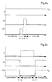
- FIG. 5a thus shows a time diagram of the evolution of the control signals TI, SH and RST applied respectively to the transistors M1, M2 and M3 of the pixel structure of FIG. 2b illustrating a first variant of the method according to the invention .
- the transistor M1 is connected in resistance configuration, the gate terminal of this transistor M1 being connected continuously to the supply voltage V DD .
- the signal TI is thus maintained at the voltage value applied to the drain of the transistor M1.
- the coupling signal SH is maintained in the high logic state so as to couple the memory node B to the source terminal of the transistor M1 (node A) during the exposure.
- the voltage present on the memory node B is therefore representative of the voltage present at the node A at the terminals of the photodiode PD.
- the signal RST applied to the gate of the transistor M3 is here continuously maintained at a low logic level so as to make this transistor M3 non-conductive and thus decouple the memory node B from the supply voltage V DD .
- the pixel thus behaves in a manner analogous to the structure illustrated in FIG. 3, that is to say that the transistor M1 behaves like a high impedance resistance crossed by the current generated by the photodiode PD.
- the current generated being of the order of fA to nA, transistor M1 operates in low mode inversion and the response of this pixel is thus also logarithmic.
- FIG. 5b shows a time diagram of the evolution of the control signals TI, SH and RST applied to the pixel structure of FIG. 2b illustrating a second variant of the method according to the invention making it possible to operate the pixel so that it presents a logarithmic response.
- the transistor M1 is also connected in resistance configuration, the gate terminal of this transistor M1 being connected to the supply voltage V DD .
- the signal TI is therefore continuously maintained at the voltage value applied to the drain of the transistor M1.
- the coupling signal SH is here maintained in the low logic state so as to decouple the memory node B from the source terminal of the transistor M1 (node A) during the exposure. As illustrated in the diagram in FIG.
- the signal SH is briefly pulsed in the high logic state (instants t3 to t4) so as to sample and store the measurement signal on the memory node B.
- the signal RST applied to the transistor M3 is also briefly pulsed in the high logic state (instants t1 to t2) so as to initialize the memory node B at a determined initialization voltage.
- the read operation according to this second variant can be undertaken in parallel with a subsequent exhibition, from when the measurement signal has been stored on memory node B.
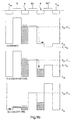
- FIG. 5c shows a time diagram of the evolution of the control signals TI, SH and RST applied to the pixel structure of FIG. 2b illustrating a third variant of the method according to the invention also making it possible to operate the pixel so that 'it presents a logarithmic response.
- the transistor M3 is connected in the resistance configuration during exposure, the gate terminal of this transistor M3 being connected to the supply voltage V DD .
- the signal RST is therefore maintained, during the exposure phase, at the voltage value applied to the drain of the transistor M3.
- the coupling signal SH is maintained in the high logic state so as to couple the memory node B to the source terminal of the transistor M1 (node A) during the exposure.
- the TI signal is kept at the low logic level during the exposure.
- the exposure continues until time t1 when the coupling signal SH as well as the signal RST are brought to a low level in order to isolate the memory node B and memorize the measurement signal on this node.
- the SH and RST signals should be simultaneously brought to the low level at time t1. Since the switching simultaneous transistors M2 and M3 is difficult to achieve in practice, we will arrange preferably so that the RST signal first goes to the low level followed by the SH signal. This would induce a slight offset on the measurement signal present on the node memory B which can be considered and tolerated during reading.
- the TI signal applied to the gate terminal of transistor M1 at a high level as soon as the measurement signal has been memorized on the memory node B (instant t2 in FIG. 5c). Indeed, the photodiode PD being decoupled, it continues to produce charge carriers which could possibly disturb the signal present on the memory node B.
- the transistor M1 operated in this way thus makes it possible to drain the charge carriers produced by the photodiode PD.
- the read operation can be undertaken using the transistors M4 and M5.
- the signal TI is brought back to its low level (time t3) then the SH and RST signals are brought back to the previous levels for the next exhibition.
- FIG. 6a thus presents a fourth variant of the method according to the present invention according to which transistor M1 is configured so that it operates at less partially at low inversion so that the pixel presents, during the phase exposure of the photodetector element, a logarithmic response for levels of illumination higher than a determined level of illumination.
- the signal TI applied to the gate terminal of the transistor M1 is switched between a first analog level, designated V 1 , greater than the supply voltage V DD plus the threshold voltage, designated V TH , of the transistor M1, and a second analog level, designated V 2 , less than or equal to the supply voltage V DD but greater than the threshold voltage V TH of the transistor M1.
- the first analog level V 1 is applied during an initialization phase forcing the voltage across the photodiode PD to the voltage V DD .
- the second analog level V 2 is applied for a determined period of time ⁇ T (instants t1 to t5) during the exposure phase.
- the nodes A and B of the pixel are decoupled during the exposure phase (and during the initialization phase), the signal SH thus being maintained at a low logic level.
- This signal SH is briefly pulsed at a high level at the end of the exposure phase (instants t4 to t5) in order to sample and store the measurement signal on the memory node B.
- the signal RST applied to the transistor M3 is also briefly pulsed in the high logic state (times t2 to t3) so as to initialize the memory node B at a determined initialization voltage.
- the read operation is undertaken in parallel with a subsequent exposure, as soon as the measurement signal has been stored on the memory node B.
- the photodiode PD is firstly released from its initialization voltage V DD .
- the gate-source voltage of the transistor M1 is such that this transistor is not conductive.
- the pixel response is thus of the linear type and the voltage V OS at the terminals of the photodiode PD decreases linearly with a slope dependent on the illumination of the pixel. If the illumination is such that the voltage V OS decreases and becomes lower than the voltage applied to the gate terminal of the transistor M1, namely the second analog level V 2 of the signal TI, the transistor M1 enters the low inversion mode and the pixel response then becomes logarithmic. In a way, a signal compression operation is performed on the pixel.
- FIG. 6b presents a fifth variant of the method according to the present invention, analogous to the variant illustrated in FIG. 6a but according to which the transistor M3 is configured so that it works at least partially in low inversion so that the pixel exhibits, during the exposure phase of the photo-detector element, a logarithmic response for levels of illumination above a level of determined illumination.
- the two analog levels V 1 and V 2 are applied to the gate terminal of the transistor M3 respectively during an initialization phase and during an exposure phase for a determined period of time ⁇ T (instants t1 to t2).
- the nodes A and B of the pixel are coupled during the exposure phase, the signal SH thus being maintained at a high logic level during this phase.
- This signal SH is brought to a low logic level (as is the signal RST) at the end of the exposure phase (instants t2 to t5) in order to isolate the memory node B and memorize the measurement signal on this memory node B.
- the signal TI applied to the gate terminal of the transistor M1 is preferably brought to a high level (at least higher than the voltage applied to the gate of transistor M2) as soon as the measurement signal has been stored on the node memory B (instant t3 in FIG. 6b) this allowing drainage, via the transistor M1, charge carriers produced by the photodiode PD.
- the read operation can be undertaken using the transistors M4 and M5.
- the signal TI is brought back to its low level (instant t4) then the SH and RST signals are brought back to the previous levels for the next exhibition as illustrated.
- the photodiode PD is first released of its initialization voltage substantially equal to V DD .
- the gate-source voltage of the transistor M3 is such that this transistor is not conductive.
- the pixel response is thus of the linear type and the voltage V OS at the terminals of the photodiode PD decreases linearly with a slope depending on the illumination of the pixel, the voltage present on the memory node B being representative of the voltage V OS .
- the transistor M3 enters low mode inversion and the pixel response then becomes logarithmic, a signal compression operation is then performed on the pixel.
- a variant of the principles of Figures 6a and 6b may consist of not switch the voltage applied to the gate terminal of transistor M1 or M3, but at switch the voltage applied to the drain of these transistors.
- Figures 7a and 7b thus illustrate first and second variants of the pixel structure of FIG. 2b can be operated so that they have a combined linear-logarithmic response.
- FIG. 7a differs in particular from the structure of FIG. 2b in that the drain terminal of the transistor M3 is connected to a supply potential V BIAS greater than the supply potential V DD .
- the structure of Figure 7b differs from the structure of Figure 2b in particular in that the drain terminal of the transistor M1 is connected to the supply potential V BIAS .
- FIG. 8a illustrates the evolution of the signals TI, SH and RST applied to the pixel structure of FIG. 7a.
- the transistor M1 is connected continuously in resistance configuration, the gate terminal of this transistor M1 being connected to the supply voltage V DD .
- the signal RST is brought to its high logic level so as to apply to the source terminal of transistor M1 a determined initialization voltage greater than the voltage d 'V DD power supply.
- the signal SH is maintained at a high logic level so as to couple the nodes A and B of the pixel.
- the nodes A and B are thus both initialized by means of the transistor M3.
- the exposure phase begins with the passage of the signal RST at the low logic level (time t1) and continues until the moment (time t2) when the signal SH is brought to a low logic level in order to isolate the memory node B and thus memorize the measurement signal on this memory node B.
- the pixel exhibits a linear response as a function of the illumination and, as soon as the voltage V OS at the terminals of the photodiode PD becomes less than the gate voltage of the transistor M1 (namely the voltage V DD ), the transistor M1 enters the low inversion mode and the pixel then has a logarithmic response.
- the measurement signal is therefore stored on the memory node B and the reading process can then start using the transistors M4 and M5.
- the charge carriers produced by the photodiode PD are drained via the transistor M1, the voltage V OS being maintained at its equilibrium level defined by the current generated by the photodiode PD.
- the signal SH is brought back to its previous high logic level, followed (instant t4) by the initialization signal RST. The the entire process is then repeated for the next acquisition.
- FIG. 8b illustrates the evolution of the signals TI, SH and RST applied to the pixel structure of FIG. 7b.
- the transistor M3 is connected in resistance configuration during the exposure phase, the gate terminal of this transistor M3 being connected to the supply voltage V DD .
- the signal TI is brought to its high logic level so as to apply, to the source terminal of the transistor M3 (at the memory node B), a voltage d 'initialization determined higher than the supply voltage V DD .
- the signal SH is maintained at a high logic level so as to couple the nodes A and B.
- the nodes A and B are thus both initialized by means of the transistor M1.
- the exposure phase begins with the passage of the signal TI at the low logic level (instant t1) and continues until the moment (instant t2) when the signals SH and RST are brought to a low logic level in order to isolate the node. memory B and thus memorize the measurement signal on this memory node B.
- the pixel exhibits a linear response as a function of the illumination and, as soon as the voltage of the memory node B becomes lower than the voltage of the gate of the transistor M3 (namely the voltage V DD ), the transistor enters the low inversion mode and the pixel then has a logarithmic response.
- the measurement signal is therefore stored on memory node B and the reading process can then begin using transistors M4 and M5. preferably as soon as the measurement signal is memorized on memory node B, it is advantageous to bring the signal TI to the high logic level (instant t3) in order to drain the carriers of charge which are produced continuously by the photodiode PD via the transistor M1.
- FIGS. 9a and 9b A particularly advantageous variant of the method according to the present invention will now be described with reference to FIGS. 9a and 9b. Besides the shutter function electronics and increased pixel dynamics, this variant also allows to increase the sensitivity of this pixel.
- this variant is analogous to the variant illustrated in FIG. 6b, with the difference that the transistor M2 is no longer operated as a switch in order to couple and decouple the nodes A and B of the pixel.
- the signal SH is brought, preferably continuously, to an intermediate analog level, designated V INT , that is to say a level located between the logic levels normally applied to switch the transistor M2.
- V INT is chosen to be lower than the analog level V 2 applied to the transistor M3 during the exposure.
- the signals TI and RST are operated in a manner essentially similar to the variant of FIG. 6b, as illustrated in the diagram of FIG. 9a.
- the signal RST is brought to its first logic level V 1 greater than the supply voltage V DD plus the threshold voltage V TH of the transistor M3, the signal TI being maintained in the logic state low during this phase.
- the photodiode PD is initialized via the transistor M3 and the transistor M2 at a voltage substantially equal to the gate voltage of the transistor M2, that is to say V INT , minus the threshold voltage V TH of this transistor M2.
- the exposure begins with the passage (instant t1) of the signal RST to its second analog level V 2 less than or equal to the supply voltage V DD but greater than the threshold voltage V TH .
- the TI signal is always kept low.
- the charge carriers produced by the photodiode PD are thus completely transferred, during the exposure phase, to the memory node B and this provided that the potential of the memory node B does not reach the level of the potential barrier defined by the transistor M2. Since these charge carriers "see” only the capacity of memory node B, they generate a greater voltage variation. By this mechanism, the sensitivity of the pixel is thus increased.
- the signal RST is brought to the low logic level in order to decouple the memory node B from the supply voltage V DD and the signal TI is simultaneously brought to a high logic level (at least higher than the voltage grid applied on the transistor M2) in order to interrupt the exposure of the pixel, or more exactly, the accumulation of charge carriers produced by the photodiode PD.
- the signal TI is at the high level, the charge carriers produced by the photodiode PD are drained via the transistor M1 and the measurement signal is stored on the memory node B.
- the transistor M1 controlled by the signal TI plays here the role of shutter control similar to the function which was fulfilled hitherto by the transistor M2.
- the read operation is undertaken as soon as the signal TI is brought to the high logic level and is followed by the ironing of the signal TI at its low level (instant t3) then (instant t4) the ironing of the signal RST to its first level analog V 1 .
- the process is then repeated according to the chronology set out above.
- FIG. 9b schematically illustrates the level of the potentials defined by the voltages applied to the gate terminals of the transistors M1, M2 and M3 during the initialization, exposure and reading phases.
- the nodes A and B are respectively initialized at voltages substantially equal to V INT - V TH and V DD .
- the exposure phase (t1 ⁇ t ⁇ t2), the charge carriers produced by the photodiode PD at node A are completely transferred to memory node B and accumulate there.
- the pixel response is first of all linear then logarithmic if the illumination is such that the voltage of the memory node B decreases and becomes lower than the gate voltage of the transistor M3, this the latter then enters the low inversion mode.
- the charge carriers produced by the photodiode PD are drained via the transistor M1 and the transfer of these charges to the memory node B is interrupted, this memory node also being decoupled from the supply voltage V DD by the transistor M3.
- the reading operation can be carried out according to a technique known to those skilled in the art under the denomination "Correlated Double Sampling" or CDS.
- CDS Code Division Multiple Sampling
- the reading operation of each line is broken down into a first reading phase of the voltage present on the memory nodes B of the pixels in a line followed by a second reading phase during which the memory nodes of the pixels in the line are reset, in principle by means of transistor M3.
- a signal formed by difference between the measured sampled voltage and the initialization voltage of the memory node is then produced for each pixel.
- the variants presented use either the transistor M1 or transistor M3 (designated as "first transistor” in the claims) for generate an at least partially logarithmic response.
- the other transistor that is to say the transistor which is not operated in low inversion mode, may not be necessary.
- the variant of FIG. 5a does not necessarily require the presence of the transistor M3.
- the transistor M1 in the variants of FIGS. 5c and 6b is not strictly necessary.
- the present invention is therefore applicable to any type of structure of pixels having an overall architecture as illustrated in FIG. 2a and which comprises at least one transistor connected, directly or indirectly, to the photo-detector element, i.e.
- n-well type photodiodes i.e. photodiodes formed in n-type wells.
- This structure offers the advantage of constitute a better obstacle to the diffusion of charge carriers than a structure of photodiode formed conventionally, for example of a simple region of diffusion of type n.
- the pixel structure used as an example to illustrate the process according to the present invention could in principle be carried out by means of a complementary p-MOS technology or if necessary include transistors additional.
- the sampling transistor M2 has essentially for the purpose of decoupling the photodiode and the memory node from the pixel and that other arrangements can be provided to fulfill this function.
Abstract
Description
La présente invention concerne généralement un capteur d'image intégré et un procédé permettant d'opérer un tel capteur d'image intégré. Plus particulièrement, la présente invention concerne un capteur d'image intégré en technologie CMOS et un procédé permettant d'opérer un tel capteur d'image CMOS avec une dynamique accrue. De tels capteurs d'image CMOS sont en particulier destinés à la réalisation de dispositifs photographiques et vidéos intégrés.The present invention generally relates to an integrated image sensor and a method for operating such an integrated image sensor. More specifically, the The present invention relates to an image sensor integrated in CMOS technology and a method for operating such a CMOS image sensor with increased dynamics. Such CMOS image sensors are in particular intended for the production of devices integrated photographic and video.
Grâce aux technologies actuelles d'intégration, il est possible de réaliser sous forme intégrée un dispositif opérationnel de prise d'images. Un tel dispositif intégré de prise d'images incorpore, sur une même puce, un composant photo-détecteur formé d'un ensemble d'éléments photo-détecteurs organisés typiquement sous forme de matrice, et un composant de traitement destiné à assurer les opérations de prise d'images et de lecture de l'information capturée par le composant photo-détecteur.Thanks to current integration technologies, it is possible to realize under integrated form an operational device for taking images. Such an integrated device of image taking incorporates, on the same chip, a photo-detector component formed by a set of photo-detector elements typically organized in the form of a matrix, and a processing component intended to ensure the operations of taking images and reading of the information captured by the photo-detector component.
Traditionnellement, les dispositifs intégrés de prise d'images font appel à des techniques de transfert de charge. Selon ces techniques, des charges photo-générées sont collectées et transférées d'une manière déterminée. Les techniques de transfert de charge les plus communes utilisent des composants CCD ("charge-coupled devices") ou des composants CID ("charge injection devices"). Bien que ces dispositifs employant ces composants aient trouvé de nombreuses applications commerciales, ceux-ci présentent néanmoins de sérieux désavantages. En particulier, ces composants font appel à des techniques de fabrication non standards, et en particulier incompatibles avec les processus de fabrication CMOS standards. Des tels composants sont donc des obstacles, en termes de coût et de facilité de fabrication, à l'intégration totale de capteurs d'images.Traditionally, integrated image capture devices have used load transfer techniques. According to these techniques, photo-generated charges are collected and transferred in a specific manner. Transfer techniques most common charges use CCD (charge-coupled devices) or CID components ("charge injection devices"). Although these devices employing these components have found many commercial applications, these present nevertheless serious disadvantages. In particular, these components use non-standard manufacturing techniques, and in particular incompatible with standard CMOS manufacturing process. Such components are therefore obstacles, in terms of cost and ease of manufacture, the full integration of image sensors.
En complément des techniques susmentionnées, un concept a été développé autour de l'utilisation de jonctions p-n semi-conducteurs comme éléments photo-détecteurs, ces jonctions étant communément dénommées photodiodes. L'avantage essentiel de tels éléments est leur parfaite compatibilité avec les processus de fabrication CMOS standard. On connaít ainsi de l'art antérieur, notamment du document "A Random Access Photodiode Array for Intelligent Image Capture" de Orly Yadid-Pecht, Ran Ginosar et Yosi Shacham Diamand, IEEE Transactions On Electron Devices, Vol. 38, no. 8, août 1991, pp. 1772-1780, incorporé ici par référence, des solutions faisant appel à des photodiodes comme éléments photo-détecteurs.In addition to the above techniques, a concept has been developed around the use of semiconductor p-n junctions as photo-detector elements, these junctions being commonly called photodiodes. The advantage essential of such elements is their perfect compatibility with manufacturing processes Standard CMOS. We thus know from the prior art, in particular from the document "A Random Access Photodiode Array for Intelligent Image Capture "by Orly Yadid-Pecht, Ran Ginosar and Yosi Shacham Diamand, IEEE Transactions On Electron Devices, Vol. 38, no. 8 August 1991, pp. 1772-1780, incorporated here by reference, solutions calling on photodiodes as photodetector elements.
Ce document décrit ainsi un capteur d'image intégré en technologie CMOS sous
forme d'une unique puce. L'architecture de ce capteur, qui est similaire à celle de
mémoires RAM, est illustrée à la figure 1. Ce capteur, indiqué généralement par la
référence numérique 1, comporte une matrice 10 de pixels agencés en M lignes et N
colonnes. Cette matrice 10 occupe la majeure partie de la surface du capteur. La lecture
d'un pixel particulier de la matrice 10 est effectué par l'adressage de la ligne et de la
colonne correspondantes. A cet effet, le capteur comprend en outre un circuit d'adressage
de ligne 20 couplé aux lignes de la matrice 10 et un bus de sortie 30 couplé aux colonnes
de la matrice 10, tous deux commandés par un circuit de commande 40.This document describes an image sensor integrated in CMOS technology under
form of a single chip. The architecture of this sensor, which is similar to that of
RAM memories, is illustrated in FIG. 1. This sensor, generally indicated by the
Chaque pixel de la matrice 10 possède une structure conforme à l'illustration de la
figure 2a. Ce pixel, indiqué généralement par la référence numérique 50 dans la figure 2a,
comporte un élément photo-détecteur PD, un premier étage A1, un moyen de stockage
C1 et un second étage A2. L'élément photo-détecteur PD est formé d'une photodiode
polarisée inverse qui opère typiquement par collecte des électrons photo-générés durant
une période dite d'intégration. Le premier étage A1 est un circuit de type "sample-and-hold"
assurant l'échantillonnage, à un temps déterminé, de la valeur de tension présente
aux bornes de la photodiode PD. Cette valeur échantillonnée est mémorisée dans le
moyen de stockage C1 qui est typiquement formé d'une capacité. On notera que la valeur
de la tension stockée sur la capacité C1 dépend de la fonction de transfert du premier
étage A1 et en particulier du rapport entre la valeur de la capacité de la photodiode PD et
de la capacité du moyen de stockage C1. Le second étage A2 permet quant à lui
d'assurer la lecture de la tension échantillonnée mémorisée dans le moyen de stockage
C1. La structure schématiquement décrite dans la figure 2a permet avantageusement la
séparation des processus de détection et de lecture.Each pixel of the
La structure générale du pixel illustrée dans la figure 2a permet ainsi de réaliser une fonction dite d'obturation électronique permettant d'exposer simultanément tous les pixels du capteur et de mémoriser, dans chaque pixel, le signal représentatif de cette exposition en vue d'une lecture ultérieure. Au moyen de cette structure, on peut ainsi réaliser un capteur d'image susceptible de permettre l'acquisition d'instantanés (ou « snap-shots ») d'une scène, c'est-à-dire un capteur parfaitement adapté pour l'acquisition d'images d'objets en mouvement relatif par rapport au capteur.The general structure of the pixel illustrated in FIG. 2a thus makes it possible to achieve a so-called electronic shutter function allowing simultaneous exposure of all pixels of the sensor and memorize, in each pixel, the signal representative of this exhibition for later reading. By means of this structure, we can thus create an image sensor capable of allowing the acquisition of snapshots (or "Snap-shots") of a scene, that is to say a sensor perfectly suited for the acquisition images of objects in relative motion relative to the sensor.
Diverses réalisations sont envisagées et présentées dans le document de l'art
antérieur susmentionné. La figure 2b montre en particulier l'une de ces réalisations dans
laquelle le pixel 50 comporte la photodiode PD polarisée inverse et cinq transistors M1 à
M5 de type n-MOS. Chaque pixel 50 comporte un noeud mémoire, désigné B, formé d'une
capacité (capacité C1) et protégé de la lumière, par exemple par une couche de
protection métallique.Various realizations are envisaged and presented in the art document
above mentioned. Figure 2b shows in particular one of these embodiments in
which the
Selon l'article susmentionné, le pixel opère selon un mode d'intégration et le transistor M1 assure l'initialisation de la photodiode PD à une tension déterminée avant chaque période d'intégration. Le transistor M2 assure l'échantillonnage de la charge accumulée par la photodiode PD et la mémorisation du signal ainsi échantillonné sur le noeud mémoire B. Ce transistor M2 assure par ailleurs un isolement ou découplage de la photodiode PD et du noeud mémoire B. Le transistor M3 assure notamment l'initialisation du noeud mémoire B à une tension déterminée. Le transistor M4 est un transistor à "source suiveuse" ("source follower transistor") et le transistor M5 est un transistor de sélection de ligne et assure, lors du processus de lecture, le transfert de la tension du transistor M4 sur un bus de sortie commun à tous les pixels dans une colonne. Les signaux appliqués sur cette structure comprennent une tension d'alimentation haute VDD et une tension d'alimentation basse VSS formant masse, un premier signal d'initialisation TI, un signal de couplage SH, un second signal d'initialisation RST, et un signal de sélection de ligne RSEL.According to the above-mentioned article, the pixel operates according to an integration mode and the transistor M1 initializes the photodiode PD at a determined voltage before each integration period. The transistor M2 ensures the sampling of the charge accumulated by the photodiode PD and the storage of the signal thus sampled on the memory node B. This transistor M2 moreover ensures an isolation or decoupling of the photodiode PD and the memory node B. The transistor M3 ensures in particular the initialization of the memory node B at a determined voltage. The transistor M4 is a "follower source transistor" and the transistor M5 is a line selection transistor and ensures, during the reading process, the transfer of the voltage from the transistor M4 on a bus. output common to all pixels in a column. The signals applied to this structure include a high supply voltage V DD and a low supply voltage V SS forming mass, a first initialization signal TI, a coupling signal SH, a second initialization signal RST, and an RSEL line selection signal.
Une première borne de la photodiode PD est connectée à la masse VSS et l'autre borne est connectées aux terminaux de source des transistors M1 et M2 dont les terminaux de grille sont respectivement commandés par les signaux TI et SH. Le noeud de connexion entre la photodiode PD et les terminaux de sources des transistors M1 et M2 sera désigné par la référence A dans la suite de la description. Les terminaux de drain des transistors M1, M3 et M4 sont connectés à la tension d'alimentation haute VDD. Le second signal d'initialisation RST est appliqué sur le terminal de grille du transistor M3. Le terminal de source du transistor M3, le terminal de drain du transistor M2 et le terminal de grille du transistor M4 sont connectés ensemble au noeud mémoire B du pixel. Le terminal de source du transistor M4 est connecté, via le transistor de sélection de ligne M5, au bus de sortie commun à tous les pixels dans une colonne. Le signal de sélection de ligne RSEL est appliqué sur le terminal de grille du transistor M5.A first terminal of the photodiode PD is connected to the ground V SS and the other terminal is connected to the source terminals of the transistors M1 and M2 whose gate terminals are respectively controlled by the signals TI and SH. The connection node between the photodiode PD and the source terminals of the transistors M1 and M2 will be designated by the reference A in the following description. The drain terminals of the transistors M1, M3 and M4 are connected to the high supply voltage V DD . The second initialization signal RST is applied to the gate terminal of the transistor M3. The source terminal of transistor M3, the drain terminal of transistor M2 and the gate terminal of transistor M4 are connected together to memory node B of the pixel. The source terminal of the transistor M4 is connected, via the line selection transistor M5, to the output bus common to all the pixels in a column. The RSEL line selection signal is applied to the gate terminal of transistor M5.
On notera que la plupart des capteurs d'images CMOS adoptent une technique d'exposition dite de « rolling shutter », c'est-à-dire que l'exposition est effectuée ligne après ligne. Cette exposition non simultanée conduit inévitablement à une distorsion de l'image, en particulier lors de l'acquisition d'une image d'un objet en mouvement.Note that most CMOS image sensors adopt a technique so-called rolling shutter exposure, that is to say that the exposure is carried out online after line. This non-simultaneous exposure inevitably leads to a distortion of the image, especially when acquiring an image of a moving object.
La structure de pixel illustrée dans les figures 2a et 2b est typiquement opérée selon un mode d'intégration, c'est-à-dire que les éléments photo-détecteurs sont tout d'abord initialisés à une tension déterminée puis soumis à une illumination durant une période de temps déterminée, les charges produites par les éléments photo-détecteurs étant accumulées ou intégrées durant cette période. Selon ce mode de fonctionnement, la réponse du pixel peut être qualifiée de linéaire. Un désavantage de ce mode de fonctionnement réside dans le fait que la dynamique du pixel est réduite.The pixel structure illustrated in Figures 2a and 2b is typically operated according to a mode of integration, that is to say that the photo-detector elements are all first initialized at a determined voltage and then subjected to illumination during a determined period of time, the charges produced by the photo-detector elements being accumulated or integrated during this period. According to this operating mode, the pixel response can be called linear. A disadvantage of this mode of how it works is that the pixel dynamics are reduced.
De nombreuses applications requièrent des capteurs d'images possédant une
grande dynamique. Afin d'accroítre la dynamique d'un capteur d'image, il est déjà connu
d'utiliser des capteurs comprenant des pixels possédant une réponse de type
logarithmique. La figure 3 présente un schéma d'un tel pixel agencé pour présenter une
réponse logarithmique. Ce pixel, indiqué globalement par la référence numérique 50,
comprend une photodiode PD polarisée inverse, et un premier et second transistor Q1 et
Q2 de type n-MOS. Une première borne de la photodiode PD est connectée à la masse
VSS et son autre borne au terminal de source du transistor Q1. Les terminaux de grille et
de drain du transistor Q1 sont connectés ensemble à un potentiel d'alimentation VDD.
Dans cette configuration, le transistor Q1, branché en résistance, est traversé par le
courant de faible intensité (de l'ordre du fA au nA) généré par la photodiode PD et opère
en conséquence en faible inversion (on dit également que ce transistor opère en
conduction infraseuil ou « subthreshold conduction »). La tension VOS aux bornes de la
photodiode PD, au noeud de connexion entre la photodiode PD et le transistor Q1,
présente de la sorte une dépendance logarithmique par rapport au courant généré sous
l'effet d'une illumination. Le transistor Q2 forme un étage de lecture du pixel (similaire au
transistor M4 de la figure 2b) et son terminal de grille est connecté au noeud de connexion
entre la photodiode PD et le transistor Q1.Many applications require image sensors with high dynamics. In order to increase the dynamics of an image sensor, it is already known to use sensors comprising pixels having a response of logarithmic type. FIG. 3 presents a diagram of such a pixel arranged to present a logarithmic response. This pixel, indicated overall by the
La configuration illustrée en figure 3 est dite à conversion continue, c'est-à-dire que la tension VOS, qui est une fonction logarithmique du courant généré par la photodiode PD, est directement convertie et est représentative de l'illumination du pixel. Contrairement aux structures de pixels à réponse dite linéaire, les charges produites par l'élément photo-détecteur ne sont pas « intégrées» durant une période dite d'intégration ou d'exposition de durée déterminée.The configuration illustrated in FIG. 3 is said to be continuous conversion, that is to say that the voltage V OS , which is a logarithmic function of the current generated by the photodiode PD, is directly converted and is representative of the illumination of the pixel. . Unlike pixel structures with a so-called linear response, the charges produced by the photo-detector element are not "integrated" during a so-called integration or exposure period of determined duration.
Un problème de la configuration illustrée à la figure 3 réside dans le fait que la variation de tension produite en fonction de l'illumination tend à être relativement faible (de l'ordre de quelques centaines de mV). Ceci rend difficile l'utilisation d'un tel pixel pour l'implémentation d'un capteur ayant un rapport signal sur bruit élevé, en particulier pour des niveaux d'illumination réduits. En outre, le temps de réponse de ce type de pixel devient très long pour de faibles illuminations où le courant photo-généré est faible.A problem with the configuration illustrated in FIG. 3 resides in the fact that the variation in voltage produced as a function of illumination tends to be relatively small (from on the order of a few hundred mV). This makes it difficult to use such a pixel to the implementation of a sensor with a high signal-to-noise ratio, in particular for reduced levels of illumination. In addition, the response time of this type of pixel becomes very long for weak illuminations where the photo-generated current is weak.
Il a ainsi également été proposé dans le document « Wide-Dynamic-Range Pixel with Combined Linear and Logarithmic Response and Increased Signal Swing », Eric C. Fox et consorts, Sensors and Camera Systems for Scientific, Industrial and Digital Photography Applications, Proceedings of SPIE Vol. 3965 (2000), pp. 4-10, une structure de pixel présentant une réponse combinée linéaire-logarithmique. Un schéma de ce pixel est illustré dans la figure 4.It has also been proposed in the document “Wide-Dynamic-Range Pixel with Combined Linear and Logarithmic Response and Increased Signal Swing ”, Eric C. Fox et al., Sensors and Camera Systems for Scientific, Industrial and Digital Photography Applications, Proceedings of SPIE Vol. 3965 (2000), pp. 4-10, a structure pixel with a combined linear-logarithmic response. A diagram of this pixel is illustrated in figure 4.
A la différence du pixel de la figure 3,-ce pixel comporte en outre un troisième transistor Q3 connecté par son terminal de source au noeud de connexion entre la photodiode PD et le premier transistor Q1 et, par son terminal de drain, à un potentiel dit d'initialisation ou reset VBIAS. L'état de conduction du transistor Q3 est commandé par le signal ΦRST appliqué sur son terminal de grille. Le potentiel d'initialisation VBIAS est supérieur au potentiel d'alimentation VDD de sorte que lorsque le signal ΦRST est à l'état logique haut, la tension VOS aux bornes de la photodiode PD est amenée à une tension telle que la tension grille-source du transistor Q1 est inférieure à la tension nécessaire pour permettre la conduction infraseuil de ce transistor Q1.Unlike the pixel of FIG. 3, this pixel further comprises a third transistor Q3 connected by its source terminal to the connection node between the photodiode PD and the first transistor Q1 and, by its drain terminal, to a potential. said initialization or reset V BIAS . The conduction state of transistor Q3 is controlled by the signal Φ RST applied to its gate terminal. The initialization potential V BIAS is greater than the supply potential V DD so that when the signal Φ RST is in the high logic state, the voltage V OS at the terminals of the photodiode PD is brought to a voltage such that the gate-source voltage of the transistor Q1 is lower than the voltage necessary to allow the infra-threshold conduction of this transistor Q1.
Dès lors que le signal ΦRST est ramené à un niveau logique bas, la tension VOS diminue linéairement sous l'effet de l'illumination jusqu'à ce que la tension grille-source du transistor Q1 atteigne un niveau tel que ce transistor opère en faible inversion. Au-delà de ce niveau, la réponse du pixel devient logarithmique de manière analogue à ce qui à déjà été mentionné en référence à la figure 3.As soon as the signal Φ RST is brought to a low logic level, the voltage V OS decreases linearly under the effect of the illumination until the gate-source voltage of the transistor Q1 reaches a level such that this transistor operates. in low inversion. Beyond this level, the pixel response becomes logarithmic in a manner analogous to what has already been mentioned with reference to FIG. 3.
De même que la structure illustrée dans la figure 3, la tension VOS aux bornes de la photodiode PD est directement appliquée sur l'entrée de l'étage de lecture. Il n'est donc pas possible d'utiliser directement ces structures pour réaliser un capteur d'image à obturation électronique adapté pour l'acquisition d'instantanés ou « snap-shots ».Like the structure illustrated in FIG. 3, the voltage V OS at the terminals of the photodiode PD is directly applied to the input of the reading stage. It is therefore not possible to directly use these structures to produce an electronically shuttered image sensor suitable for the acquisition of snapshots or "snap-shots".
Un but de la présente invention est ainsi de proposer un procédé permettant d'opérer un capteur d'image à obturation électronique du type susmentionné possédant une structure de pixel conforme aux illustrations des figures 2a et 2b et ceci avec une dynamique accrue.An object of the present invention is thus to propose a method allowing to operate an electronic shutter image sensor of the aforementioned type having a pixel structure in accordance with the illustrations in FIGS. 2a and 2b and this with a increased dynamics.
Afin de répondre à ce but, la présente invention a pour objet un procédé
permettant d'opérer un capteur d'image CMOS dont les caractéristiques sont énoncées
dans la revendication 1.In order to meet this aim, the present invention relates to a method
allowing to operate a CMOS image sensor whose characteristics are stated
in
La présente invention à également pour objet un capteur d'image CMOS dont les caractéristiques sont énoncées dans la revendication indépendante 15.The present invention also relates to a CMOS image sensor whose Features are set out in independent claim 15.
Des modes de réalisations avantageux de la présente invention font l'objet des revendications dépendantes.Advantageous embodiments of the present invention are the subject of dependent claims.
Selon certains modes de réalisation particuliers de l'invention, il est ainsi proposé un capteur d'image ainsi que divers procédés permettant d'opérer un tel capteur d'image à obturation électronique de sorte que chaque pixel présente une réponse combinée linéaire-logarithmique.According to certain particular embodiments of the invention, it is thus proposed an image sensor and various methods for operating such an image sensor electronically shuttered so each pixel has a combined response linear-logarithmic.
Selon un autre mode de réalisation particulièrement avantageux, il est également proposé un capteur d'image ainsi qu'un procédé permettant d'opérer un tel capteur à obturation électronique de sorte que chaque pixel présente une réponse combinée linéaire-logarithmique ainsi qu'une sensibilité accrue.According to another particularly advantageous embodiment, it is also proposed an image sensor as well as a method for operating such a sensor at electronic shutter so that each pixel has a combined response linear-logarithmic as well as increased sensitivity.
Un avantage de la présente invention réside dans le fait que la dynamique d'un capteur d'image à obturation électronique utilisant notamment une structure de pixel telle que la structure illustrée dans la figure 2b est augmentée. An advantage of the present invention lies in the fact that the dynamics of a electronically shuttered image sensor using in particular a pixel structure such that the structure illustrated in Figure 2b is increased.
D'autres caractéristiques et avantages de la présente invention apparaítront plus clairement à la lecture de la description détaillée qui suit, faite en référence aux dessins annexés donnés à titre d'exemples non limitatifs et dans lesquels :
- la figure 1, déjà présentée, illustre schématiquement l'architecture conventionnelle d'un capteur d'image CMOS ;
- les figures 2a et 2b, déjà présentées, illustrent respectivement un schéma de principe et un schéma détaillé d'une structure connue d'un pixel du capteur d'image CMOS de la figure 1 ;
- la figure 3, déjà présentée, montre un schéma détaillé d'une structure de pixel connue à réponse logarithmique ;
- la figure 4, déjà présentée, montre un schéma détaillé d'une structure de pixel connue à réponse combinée linéaire-logarithmique ;
- les figures 5a à 5c montrent des diagrammes illustrant des première, deuxième et troisième variantes du procédé selon l'invention permettant d'opérer la structure de la figure 2b de sorte qu'elle présente, outre la fonction d'obturation électronique, une réponse de type logarithmique ;
- les figures 6a et 6b montrent des diagrammes illustrant des quatrième et cinquième variantes du procédé selon l'invention permettant d'opérer la structure de la figure 2b de sorte qu'elle présente, outre la fonction d'obturation électronique, une réponse combinée linéaire-logarithmique ;
- les figures 7a et 7b illustrent des première et deuxième variantes de la structure de pixel de la figure 2b pouvant être opérées de sorte qu'elles présentent une réponse combinée linéaire-logarithmique ;
- les figures 8a et 8b montrent des diagrammes illustrant des sixième et septième variantes du procédé selon l'invention permettant respectivement d'opérer les structures de pixels des figures 7a et 7b de sorte qu'elles présentent une réponse combinée linéaire-logarithmique ;
- la figure 9a montre un diagramme illustrant une huitième variante particulièrement avantageuse du procédé selon l'invention permettant d'opérer la structure de la figure 2b de sorte qu'elle présente, outre la fonction d'obturation électronique, une réponse combinée linéaire-logarithmique ainsi qu'une sensibilité accrue ; et
- la figure 9b montre les niveaux de potentiels engendrés par les tensions appliquées sur les grilles des transistors de la structure de la figure 2b opérée selon la huitième variante illustré dans la figure 9a.
- FIG. 1, already presented, schematically illustrates the conventional architecture of a CMOS image sensor;
- Figures 2a and 2b, already presented, respectively illustrate a block diagram and a detailed diagram of a known structure of a pixel of the CMOS image sensor of Figure 1;
- FIG. 3, already presented, shows a detailed diagram of a known pixel structure with logarithmic response;
- FIG. 4, already presented, shows a detailed diagram of a known pixel structure with combined linear-logarithmic response;
- FIGS. 5a to 5c show diagrams illustrating first, second and third variants of the method according to the invention making it possible to operate the structure of FIG. 2b so that it exhibits, in addition to the electronic shutter function, logarithmic type;
- FIGS. 6a and 6b show diagrams illustrating fourth and fifth variants of the method according to the invention making it possible to operate the structure of FIG. 2b so that it has, in addition to the electronic shutter function, a combined linear response - logarithmic;
- FIGS. 7a and 7b illustrate first and second variants of the pixel structure of FIG. 2b which can be operated so that they have a combined linear-logarithmic response;
- FIGS. 8a and 8b show diagrams illustrating sixth and seventh variants of the method according to the invention making it possible respectively to operate the pixel structures of FIGS. 7a and 7b so that they have a combined linear-logarithmic response;
- FIG. 9a shows a diagram illustrating an eighth particularly advantageous variant of the method according to the invention making it possible to operate the structure of FIG. 2b so that it has, in addition to the electronic shutter function, a combined linear-logarithmic response as well increased sensitivity; and
- FIG. 9b shows the potential levels generated by the voltages applied to the gates of the transistors of the structure of FIG. 2b operated according to the eighth variant illustrated in FIG. 9a.
On décrira maintenant, au moyen des figures, diverses variantes du procédé selon
la présente invention permettant d'opérer le pixel 50 de la figure 2b de sorte qu'il présente
un réponse logarithmique pour des niveaux d'illumination supérieurs à un niveau
d'illumination déterminé.We will now describe, by means of the figures, various variants of the process according to
the present invention making it possible to operate the
On comprendra que les diverses variantes de procédé selon la présente invention ne sont pas limitées à l'opération d'une structure telle que la structure illustrée à la figure 2b, mais peuvent être appliquées de manière analogue à tout type de structure se présentant schématiquement sous la forme de la structure illustrée à la figure 2a, c'est-à-dire une structure comportant un élément photo-détecteur et un moyen de stockage susceptible d'être couplé à l'élément photo-détecteur à un instant déterminé afin de produire et mémoriser un signal de mesure représentatif des porteurs de charge produits par l'élément photo-détecteur au cours de l'exposition, cette structure présentant au moins un transistor MOS connecté (directement ou indirectement) par son terminal de drain ou de source à l'élément photo-détecteur. La structure de la figure 2b constitue néanmoins une structure simple et particulièrement avantageuse. A ce titre, on constatera que le transistor M1 ou le transistor M3 peut être configuré pour fonctionner en mode de faible inversion, le transistor M1 étant directement connecté à la photodiode PD alors que le transistor M3 est connecté à cette photodiode PD via le transistor de couplage M2. On verra que cette possibilité d'utiliser indépendamment le transistor M1 ou M3 assure une grande flexibilité d'utilisation.It will be understood that the various variants of the process according to the present invention are not limited to the operation of a structure such as the structure illustrated in the figure 2b, but can be applied analogously to any type of structure schematically showing in the form of the structure illustrated in FIG. 2a, that is to say a structure comprising a photodetector element and a storage means capable of being coupled to the photodetector element at a determined time in order to generate and store a measurement signal representative of the charge carriers produced by the photo-detector element during the exposure, this structure having at least a MOS transistor connected (directly or indirectly) by its drain terminal or source to the photo-detector element. The structure of Figure 2b nevertheless constitutes a simple and particularly advantageous structure. As such, we will see that the transistor M1 or transistor M3 can be configured to operate in low mode inversion, the transistor M1 being directly connected to the photodiode PD while the transistor M3 is connected to this photodiode PD via the coupling transistor M2. We will see that this possibility of independently using the transistor M1 or M3 ensures a great flexibility of use.
La figure 5a montre ainsi un diagramme temporel de l'évolution des signaux de commande TI, SH et RST appliqués respectivement sur les transistors M1, M2 et M3 de la structure de pixel de la figure 2b illustrant une première variante du procédé selon l'invention. Selon cette première variante, le transistor M1 est branché en configuration de résistance, le terminal de grille de ce transistor M1 étant branché en continu à la tension d'alimentation VDD. Le signal TI est ainsi maintenu à la valeur de tension appliquée sur le drain du transistor M1. Selon cette première variante, le signal de couplage SH est maintenu à l'état logique haut de manière à coupler le noeud mémoire B au terminal de source du transistor M1 (noeud A) durant l'exposition. La tension présente sur le noeud mémoire B est donc représentative de la tension présente au noeud A aux bornes de la photodiode PD. Le signal RST appliqué sur la grille du transistor M3 est ici maintenu en continu à un niveau logique bas de manière à rendre non-conducteur ce transistor M3 et ainsi découpler le noeud mémoire B de la tension d'alimentation VDD.FIG. 5a thus shows a time diagram of the evolution of the control signals TI, SH and RST applied respectively to the transistors M1, M2 and M3 of the pixel structure of FIG. 2b illustrating a first variant of the method according to the invention . According to this first variant, the transistor M1 is connected in resistance configuration, the gate terminal of this transistor M1 being connected continuously to the supply voltage V DD . The signal TI is thus maintained at the voltage value applied to the drain of the transistor M1. According to this first variant, the coupling signal SH is maintained in the high logic state so as to couple the memory node B to the source terminal of the transistor M1 (node A) during the exposure. The voltage present on the memory node B is therefore representative of the voltage present at the node A at the terminals of the photodiode PD. The signal RST applied to the gate of the transistor M3 is here continuously maintained at a low logic level so as to make this transistor M3 non-conductive and thus decouple the memory node B from the supply voltage V DD .
Durant l'exposition, le pixel se comporte ainsi de manière analogue à la structure illustrée dans la figure 3, c'est-à-dire que le transistor M1 se comporte comme une résistance de haute impédance traversée par le courant générée par la photodiode PD. Le courant généré étant de l'ordre du fA au nA, le transistor M1 opère en mode de faible inversion et la réponse de ce pixel est ainsi également logarithmique.During the exposure, the pixel thus behaves in a manner analogous to the structure illustrated in FIG. 3, that is to say that the transistor M1 behaves like a high impedance resistance crossed by the current generated by the photodiode PD. The current generated being of the order of fA to nA, transistor M1 operates in low mode inversion and the response of this pixel is thus also logarithmic.
L'exposition se prolonge jusqu'au stade (instant t1) où le signal SH est amené à un niveau bas découplant ainsi le noeud mémoire B de la photodiode PD, le signal de mesure étant alors mémorisé sur la capacité de stockage C1. L'opération de lecture peut alors être entreprise au moyen des transistors M4 et M5. Une nouvelle phase d'exposition débute par le repassage du signal SH à son niveau haut (instant t2).The exposure continues until the stage (instant t1) where the signal SH is brought to a low level thus decoupling the memory node B of the photodiode PD, the measurement signal then being memorized on the storage capacity C1. The read operation can then be undertaken by means of transistors M4 and M5. A new exhibition phase begins by ironing the signal SH at its high level (instant t2).
La figure 5b montre un diagramme temporel de l'évolution des signaux de commande TI, SH et RST appliqués sur la structure de pixel de la figure 2b illustrant une deuxième variante du procédé selon l'invention permettant d'opérer le pixel de sorte qu'il présente une réponse logarithmique. Selon cette deuxième variante, le transistor M1 est également branché en configuration de résistance, le terminal de grille de ce transistor M1 étant branché à la tension d'alimentation VDD. Le signal TI est donc maintenu en continu à la valeur de tension appliquée sur le drain du transistor M1. Le signal de couplage SH est ici maintenu à l'état logique bas de manière à découpler le noeud mémoire B du terminal de source du transistor M1 (noeud A) durant l'exposition. Comme illustré dans le diagramme de la figure 5b, le signal SH est brièvement pulsé à l'état logique haut (instants t3 à t4) de manière à échantillonner et mémoriser le signal de mesure sur le noeud mémoire B. Avant le passage du signal SH à l'état haut, le signal RST appliqué sur le transistor M3 est également brièvement pulsé à l'état logique haut (instants t1 à t2) de manière à initialiser le noeud mémoire B à une tension d'initialisation déterminée.FIG. 5b shows a time diagram of the evolution of the control signals TI, SH and RST applied to the pixel structure of FIG. 2b illustrating a second variant of the method according to the invention making it possible to operate the pixel so that it presents a logarithmic response. According to this second variant, the transistor M1 is also connected in resistance configuration, the gate terminal of this transistor M1 being connected to the supply voltage V DD . The signal TI is therefore continuously maintained at the voltage value applied to the drain of the transistor M1. The coupling signal SH is here maintained in the low logic state so as to decouple the memory node B from the source terminal of the transistor M1 (node A) during the exposure. As illustrated in the diagram in FIG. 5b, the signal SH is briefly pulsed in the high logic state (instants t3 to t4) so as to sample and store the measurement signal on the memory node B. Before the passage of the signal SH in the high state, the signal RST applied to the transistor M3 is also briefly pulsed in the high logic state (instants t1 to t2) so as to initialize the memory node B at a determined initialization voltage.
Contrairement à la variante illustrée dans la figure 5a, l'opération de lecture selon cette deuxième variante peut être entreprise en parallèle à une exposition ultérieure, dès lors que le signal de mesure a été mémorisé sur le noeud mémoire B.Unlike the variant illustrated in Figure 5a, the read operation according to this second variant can be undertaken in parallel with a subsequent exhibition, from when the measurement signal has been stored on memory node B.
La figure 5c montre un diagramme temporel de l'évolution des signaux de commande TI, SH et RST appliqués sur la structure de pixel de la figure 2b illustrant une troisième variante du procédé selon l'invention permettant également d'opérer le pixel de sorte qu'il présente une réponse logarithmique. Selon cette troisième variante, et contrairement aux variantes précédentes, le transistor M3 est branché en configuration de résistance durant l'exposition, le terminal de grille de ce transistor M3 étant branché à la tension d'alimentation VDD. Le signal RST est donc maintenu, durant la phase d'exposition, à la valeur de tension appliquée sur le drain du transistor M3. Le signal de couplage SH est maintenu à l'état logique haut de manière à coupler le noeud mémoire B au terminal de source du transistor M1 (noeud A) durant l'exposition. Le signal TI est quant à lui maintenu au niveau logique bas durant l'exposition.FIG. 5c shows a time diagram of the evolution of the control signals TI, SH and RST applied to the pixel structure of FIG. 2b illustrating a third variant of the method according to the invention also making it possible to operate the pixel so that 'it presents a logarithmic response. According to this third variant, and unlike the previous variants, the transistor M3 is connected in the resistance configuration during exposure, the gate terminal of this transistor M3 being connected to the supply voltage V DD . The signal RST is therefore maintained, during the exposure phase, at the voltage value applied to the drain of the transistor M3. The coupling signal SH is maintained in the high logic state so as to couple the memory node B to the source terminal of the transistor M1 (node A) during the exposure. The TI signal is kept at the low logic level during the exposure.
L'exposition se prolonge jusqu'à l'instant t1 où le signal de couplage SH ainsi que le signal RST sont amenés à un niveau bas afin d'isoler le noeud mémoire B et mémoriser le signal de mesure sur ce noeud. Idéalement, les signaux SH et RST devraient être amenés simultanément au niveau bas à l'instant t1. Etant donné que la commutation simultanée des transistors M2 et M3 est difficile à réaliser en pratique, on s'arrangera préférablement pour que le signal RST passe tout d'abord au niveau bas suivi par le signal SH. Ceci induirait un léger offset sur le signal de mesure présent sur le noeud mémoire B qui pourra être considéré et toléré lors de la lecture.The exposure continues until time t1 when the coupling signal SH as well as the signal RST are brought to a low level in order to isolate the memory node B and memorize the measurement signal on this node. Ideally, the SH and RST signals should be simultaneously brought to the low level at time t1. Since the switching simultaneous transistors M2 and M3 is difficult to achieve in practice, we will arrange preferably so that the RST signal first goes to the low level followed by the SH signal. This would induce a slight offset on the measurement signal present on the node memory B which can be considered and tolerated during reading.
En outre, il convient préférablement de faire passer le signal TI appliqué sur le terminal de grille du transistor M1 à un niveau haut dès lors que le signal de mesure a été mémorisé sur le noeud mémoire B (instant t2 dans la figure 5c). En effet, la photodiode PD étant découplée, celle-ci continue à produire des porteurs de charge qui pourraient éventuellement perturber le signal présent sur le noeud mémoire B. Le transistor M1 opéré de la sorte permet ainsi de drainer les porteurs de charge produits par la photodiode PD.In addition, it is preferable to pass the TI signal applied to the gate terminal of transistor M1 at a high level as soon as the measurement signal has been memorized on the memory node B (instant t2 in FIG. 5c). Indeed, the photodiode PD being decoupled, it continues to produce charge carriers which could possibly disturb the signal present on the memory node B. The transistor M1 operated in this way thus makes it possible to drain the charge carriers produced by the photodiode PD.
A partir de l'instant t2, l'opération de lecture peut être entreprise au moyen des transistors M4 et M5. Au terme de l'opération de lecture le signal TI est ramené à son niveau bas (instant t3) puis les signaux SH et RST sont ramenés aux niveaux précédents en vue de la prochaine exposition.From time t2, the read operation can be undertaken using the transistors M4 and M5. At the end of the read operation, the signal TI is brought back to its low level (time t3) then the SH and RST signals are brought back to the previous levels for the next exhibition.
Les variantes qui vont maintenant être présentées en référence aux figures 6a et 6b constituent des variantes avantageuses permettant d'opérer la structure illustrée en figure 2b de manière à ce qu'elle présente une réponse combinée linéaire-logarithmique.The variants which will now be presented with reference to FIGS. 6a and 6b constitute advantageous variants making it possible to operate the structure illustrated in Figure 2b so that it presents a combined linear-logarithmic response.
La figure 6a présente ainsi une quatrième variante du procédé selon la présente invention selon laquelle le transistor M1 est configuré de manière à ce qu'il fonctionne au moins partiellement en faible inversion de sorte que le pixel présente, lors de la phase d'exposition de l'élément photo-détecteur, une réponse logarithmique pour des niveaux d'illumination supérieurs à un niveau d'illumination déterminé.FIG. 6a thus presents a fourth variant of the method according to the present invention according to which transistor M1 is configured so that it operates at less partially at low inversion so that the pixel presents, during the phase exposure of the photodetector element, a logarithmic response for levels of illumination higher than a determined level of illumination.
Comme illustré dans le diagramme de la figure 6a, le signal TI appliqué sur le terminal de grille du transistor M1 est commuté entre un premier niveau analogique, désigné V1, supérieur à la tension d'alimentation VDD plus la tension de seuil, désignée VTH, du transistor M1, et un second niveau analogique, désigné V2, inférieur ou égal à la tension d'alimentation VDD mais supérieur à la tension de seuil VTH du transistor M1. Le premier niveau analogique V1 est appliqué durant une phase d'initialisation forçant la tension aux bornes de la photodiode PD à la tension VDD. Le second niveau analogique V2 est appliqué pour une période de temps déterminée ΔT (instants t1 à t5) durant la phase d'exposition. Selon cette variante, les noeuds A et B du pixel sont découplés durant la phase d'exposition (et durant la phase d'initialisation), le signal SH étant ainsi maintenu à un niveau logique bas. Ce signal SH est brièvement pulsé à un niveau haut au terme de la phase d'exposition (instants t4 à t5) afin d'échantillonner et mémoriser le signal de mesure sur le noeud mémoire B. Avant le passage du signal SH à l'état haut, le signal RST appliqué sur le transistor M3 est également brièvement pulsé à l'état logique haut (instants t2 à t3) de manière à initialiser le noeud mémoire B à une tension d'initialisation déterminée. L'opération de lecture est entreprise en parallèle à une exposition ultérieure, dès lors que le signal de mesure a été mémorisé sur le noeud mémoire B. As illustrated in the diagram in FIG. 6a, the signal TI applied to the gate terminal of the transistor M1 is switched between a first analog level, designated V 1 , greater than the supply voltage V DD plus the threshold voltage, designated V TH , of the transistor M1, and a second analog level, designated V 2 , less than or equal to the supply voltage V DD but greater than the threshold voltage V TH of the transistor M1. The first analog level V 1 is applied during an initialization phase forcing the voltage across the photodiode PD to the voltage V DD . The second analog level V 2 is applied for a determined period of time ΔT (instants t1 to t5) during the exposure phase. According to this variant, the nodes A and B of the pixel are decoupled during the exposure phase (and during the initialization phase), the signal SH thus being maintained at a low logic level. This signal SH is briefly pulsed at a high level at the end of the exposure phase (instants t4 to t5) in order to sample and store the measurement signal on the memory node B. Before the signal SH goes to state. high, the signal RST applied to the transistor M3 is also briefly pulsed in the high logic state (times t2 to t3) so as to initialize the memory node B at a determined initialization voltage. The read operation is undertaken in parallel with a subsequent exposure, as soon as the measurement signal has been stored on the memory node B.
Selon cette quatrième variante de l'invention, dès lors que le signal TI est amené de son premier à son second niveau analogique (instant t1), la photodiode PD est tout d'abord libérée de sa tension d'initialisation VDD. A cet instant, la tension grille-source du transistor M1 est telle que ce transistor n'est pas conducteur. La réponse du pixel est ainsi de type linéaire et la tension VOS aux bornes de la photodiode PD décroít linéairement avec une pente dépendant de l'illumination du pixel. Si l'illumination est telle que la tension VOS décroít et devient inférieure à la tension appliquée sur le terminal de grille du transistor M1, à savoir le second niveau analogique V2 du signal TI, le transistor M1 entre en mode de faible inversion et la réponse du pixel devient alors de type logarithmique. En quelque sorte, une opération de compression du signal est opérée sur le pixel.According to this fourth variant of the invention, as soon as the signal TI is brought from its first to its second analog level (instant t1), the photodiode PD is firstly released from its initialization voltage V DD . At this instant, the gate-source voltage of the transistor M1 is such that this transistor is not conductive. The pixel response is thus of the linear type and the voltage V OS at the terminals of the photodiode PD decreases linearly with a slope dependent on the illumination of the pixel. If the illumination is such that the voltage V OS decreases and becomes lower than the voltage applied to the gate terminal of the transistor M1, namely the second analog level V 2 of the signal TI, the transistor M1 enters the low inversion mode and the pixel response then becomes logarithmic. In a way, a signal compression operation is performed on the pixel.
La figure 6b présente une cinquième variante du procédé selon la présente invention, analogue à la variante illustrée en figure 6a mais selon laquelle le transistor M3 est configuré de manière à ce qu'il fonctionne au moins partiellement en faible inversion de sorte que le pixel présente, lors de la phase d'exposition de l'élément photo-détecteur, une réponse logarithmique pour des niveaux d'illumination supérieurs à un niveau d'illumination déterminé.FIG. 6b presents a fifth variant of the method according to the present invention, analogous to the variant illustrated in FIG. 6a but according to which the transistor M3 is configured so that it works at least partially in low inversion so that the pixel exhibits, during the exposure phase of the photo-detector element, a logarithmic response for levels of illumination above a level of determined illumination.
Comme illustré dans le diagramme de la figure 6b, les deux niveaux analogiques V1 et V2 sont appliqués sur le terminal de grille du transistor M3 respectivement durant une phase d'initialisation et durant une phase d'exposition pour une période de temps déterminée ΔT (instants t1 à t2). Selon cette variante, les noeuds A et B du pixel sont couplés durant la phase d'exposition, le signal SH étant ainsi maintenu à un niveau logique haut durant cette phase. Ce signal SH est amené à un niveau logique bas (de même que le signal RST) au terme de la phase d'exposition (instants t2 à t5) afin d'isoler le noeud mémoire B et mémoriser le signal de mesure sur ce noeud mémoire B.As illustrated in the diagram in FIG. 6b, the two analog levels V 1 and V 2 are applied to the gate terminal of the transistor M3 respectively during an initialization phase and during an exposure phase for a determined period of time ΔT (instants t1 to t2). According to this variant, the nodes A and B of the pixel are coupled during the exposure phase, the signal SH thus being maintained at a high logic level during this phase. This signal SH is brought to a low logic level (as is the signal RST) at the end of the exposure phase (instants t2 to t5) in order to isolate the memory node B and memorize the measurement signal on this memory node B.
En outre, le signal TI appliqué sur le terminal de grille du transistor M1 est préférablement amené à un niveau haut (au moins supérieur à la tension appliquée sur la grille du transistor M2) dès lors que le signal de mesure a été mémorisé sur le noeud mémoire B (instant t3 dans la figure 6b) ceci permettant un drainage, via le transistor M1, des porteurs de charge produits par la photodiode PD.In addition, the signal TI applied to the gate terminal of the transistor M1 is preferably brought to a high level (at least higher than the voltage applied to the gate of transistor M2) as soon as the measurement signal has been stored on the node memory B (instant t3 in FIG. 6b) this allowing drainage, via the transistor M1, charge carriers produced by the photodiode PD.
A partir de l'instant t3, l'opération de lecture peut être entreprise au moyen des transistors M4 et M5. Au terme de l'opération de lecture le signal TI est ramené à son niveau bas (instant t4) puis les signaux SH et RST sont ramenés aux niveaux précédents en vue de la prochaine exposition comme illustré.From time t3, the read operation can be undertaken using the transistors M4 and M5. At the end of the read operation, the signal TI is brought back to its low level (instant t4) then the SH and RST signals are brought back to the previous levels for the next exhibition as illustrated.
De manière analogue à la variante de la figure 6a, selon cette cinquième variante de l'invention, dès lors que le signal RST est amené de son premier à son second niveau analogique (instant t1), la photodiode PD est tout d'abord libérée de sa tension d'initialisation sensiblement égale à VDD. A cet instant, la tension grille-source du transistor M3 est telle que ce transistor n'est pas conducteur. La réponse du pixel est ainsi de type linéaire et la tension VOS aux bornes de la photodiode PD décroít linéairement avec une pente dépendant de l'illumination du pixel, la tension présente sur le noeud mémoire B étant représentative de la tension VOS. Si l'illumination est telle que la tension au noeud mémoire B décroít et devient inférieure à la tension appliquée sur le terminal de grille du transistor M3, à savoir le second niveau analogique V2 du signal RST, le transistor M3 entre en mode de faible inversion et la réponse du pixel devient alors de type logarithmique, une opération de compression du signal est alors opérée sur le pixel.Analogously to the variant of FIG. 6a, according to this fifth variant of the invention, as soon as the RST signal is brought from its first to its second analog level (instant t1), the photodiode PD is first released of its initialization voltage substantially equal to V DD . At this instant, the gate-source voltage of the transistor M3 is such that this transistor is not conductive. The pixel response is thus of the linear type and the voltage V OS at the terminals of the photodiode PD decreases linearly with a slope depending on the illumination of the pixel, the voltage present on the memory node B being representative of the voltage V OS . If the illumination is such that the voltage at the memory node B decreases and becomes lower than the voltage applied to the gate terminal of the transistor M3, namely the second analog level V 2 of the signal RST, the transistor M3 enters low mode inversion and the pixel response then becomes logarithmic, a signal compression operation is then performed on the pixel.
Une variante des principes des figures 6a et 6b peut consister à non pas commuter la tension appliquée sur le terminal de grille du transistor M1 ou M3, mais à commuter la tension appliquée sur le drain de ces transistors. Les figures 7a et 7b illustrent ainsi des première et deuxième variantes de la structure de pixel de la figure 2b pouvant être opérées de sorte qu'elles présentent une réponse combinée linéaire-logarithmique.A variant of the principles of Figures 6a and 6b may consist of not switch the voltage applied to the gate terminal of transistor M1 or M3, but at switch the voltage applied to the drain of these transistors. Figures 7a and 7b thus illustrate first and second variants of the pixel structure of FIG. 2b can be operated so that they have a combined linear-logarithmic response.
La structure de la figure 7a diffère notamment de la structure de la figure 2b en ce que le terminal de drain du transistor M3 est relié à un potentiel d'alimentation VBIAS supérieur au potentiel d'alimentation VDD. La structure de la figure 7b diffère quant à elle de la structure de la figure 2b notamment en ce que le terminal de drain du transistor M1 est relié au potentiel d'alimentation VBIAS.The structure of FIG. 7a differs in particular from the structure of FIG. 2b in that the drain terminal of the transistor M3 is connected to a supply potential V BIAS greater than the supply potential V DD . The structure of Figure 7b differs from the structure of Figure 2b in particular in that the drain terminal of the transistor M1 is connected to the supply potential V BIAS .
Le diagramme de la figure 8a illustre l'évolution des signaux TI, SH et RST appliqués sur la structure de pixel de la figure 7a. De manière analogue à la variante de la figure 5a, le transistor M1 est branché en continu en configuration de résistance, le terminal de grille de ce transistor M1 étant branché à la tension d'alimentation VDD. Durant une première phase d'initialisation (jusqu'à l'instant t1), le signal RST est amené à son niveau logique haut de manière à appliquer sur le terminal de source du transistor M1 une tension d'initialisation déterminée supérieure à la tension d'alimentation VDD. Durant cette étape d'initialisation, ainsi que durant la phase d'exposition du pixel, le signal SH est maintenu à un niveau logique haut de manière à coupler les noeuds A et B du pixel. Les noeuds A et B sont ainsi tous deux initialisés au moyen du transistor M3.The diagram of FIG. 8a illustrates the evolution of the signals TI, SH and RST applied to the pixel structure of FIG. 7a. Analogously to the variant of FIG. 5a, the transistor M1 is connected continuously in resistance configuration, the gate terminal of this transistor M1 being connected to the supply voltage V DD . During a first initialization phase (until time t1), the signal RST is brought to its high logic level so as to apply to the source terminal of transistor M1 a determined initialization voltage greater than the voltage d 'V DD power supply. During this initialization step, as well as during the pixel exposure phase, the signal SH is maintained at a high logic level so as to couple the nodes A and B of the pixel. The nodes A and B are thus both initialized by means of the transistor M3.
La phase d'exposition débute par le passage du signal RST au niveau logique bas (instant t1) et se poursuit jusqu'au moment (instant t2) où le signal SH est amené à un niveau logique bas afin d'isoler le noeud mémoire B et ainsi mémoriser le signal de mesure sur ce noeud mémoire B. Durant cette étape d'exposition, le pixel présente une réponse linéaire en fonction de l'illumination et, dès lors que la tension VOS aux bornes de la photodiode PD devient inférieure à la tension de grille du transistor M1 (à savoir la tension VDD), le transistor M1 entre en mode de faible inversion et le pixel présente alors une réponse logarithmique. The exposure phase begins with the passage of the signal RST at the low logic level (time t1) and continues until the moment (time t2) when the signal SH is brought to a low logic level in order to isolate the memory node B and thus memorize the measurement signal on this memory node B. During this exposure step, the pixel exhibits a linear response as a function of the illumination and, as soon as the voltage V OS at the terminals of the photodiode PD becomes less than the gate voltage of the transistor M1 (namely the voltage V DD ), the transistor M1 enters the low inversion mode and the pixel then has a logarithmic response.
A l'instant t2, le signal de mesure est donc mémorisé sur le noeud mémoire B et le processus de lecture peut alors débuter à l'aide des transistors M4 et M5. Dans ce cas, les porteurs de charge produits par la photodiode PD sont drainés via le transistor M1, la tension VOS étant maintenue à son niveau d'équilibre défini par le courant généré par la photodiode PD.At time t2, the measurement signal is therefore stored on the memory node B and the reading process can then start using the transistors M4 and M5. In this case, the charge carriers produced by the photodiode PD are drained via the transistor M1, the voltage V OS being maintained at its equilibrium level defined by the current generated by the photodiode PD.
Au terme du processus de lecture (instant t3), le signal SH est ramené à son niveau logique haut précédent, suivi (instant t4) par le signal d'initialisation RST. Le processus entier est alors répété pour l'acquisition suivante.At the end of the reading process (instant t3), the signal SH is brought back to its previous high logic level, followed (instant t4) by the initialization signal RST. The the entire process is then repeated for the next acquisition.
Le diagramme de la figure 8b illustre l'évolution des signaux TI, SH et RST appliqués sur la structure de pixel de la figure 7b. De manière analogue à la variante de la figure 5c, le transistor M3 est branché en configuration de résistance durant la phase d'exposition, le terminal de grille de ce transistor M3 étant relié à la tension d'alimentation VDD. Durant une première phase d'initialisation (jusqu'à l'instant t1), le signal TI est amené à son niveau logique haut de manière à appliquer, sur le terminal de source du transistor M3 (au noeud mémoire B), une tension d'initialisation déterminée supérieure à la tension d'alimentation VDD. Durant cette étape d'initialisation, le signal SH est maintenu à un niveau logique haut de manière à coupler les noeuds A et B. Les noeuds A et B sont ainsi tous deux initialisés au moyen du transistor M1.The diagram of FIG. 8b illustrates the evolution of the signals TI, SH and RST applied to the pixel structure of FIG. 7b. Analogously to the variant of FIG. 5c, the transistor M3 is connected in resistance configuration during the exposure phase, the gate terminal of this transistor M3 being connected to the supply voltage V DD . During a first initialization phase (until time t1), the signal TI is brought to its high logic level so as to apply, to the source terminal of the transistor M3 (at the memory node B), a voltage d 'initialization determined higher than the supply voltage V DD . During this initialization step, the signal SH is maintained at a high logic level so as to couple the nodes A and B. The nodes A and B are thus both initialized by means of the transistor M1.
La phase d'exposition débute par le passage du signal TI au niveau logique bas (instant t1) et se poursuit jusqu'au moment (instant t2) où les signaux SH et RST sont amenés à un niveau logique bas afin d'isoler le noeud mémoire B et ainsi mémoriser le signal de mesure sur ce noeud mémoire B. Durant cette étape d'exposition, le pixel présente une réponse linéaire en fonction de l'illumination et, dès lors que la tension du noeud mémoire B devient inférieure à la tension de grille du transistor M3 (à savoir la tension VDD), le transistor entre en mode de faible inversion et le pixel présente alors une réponse logarithmique.The exposure phase begins with the passage of the signal TI at the low logic level (instant t1) and continues until the moment (instant t2) when the signals SH and RST are brought to a low logic level in order to isolate the node. memory B and thus memorize the measurement signal on this memory node B. During this exposure step, the pixel exhibits a linear response as a function of the illumination and, as soon as the voltage of the memory node B becomes lower than the voltage of the gate of the transistor M3 (namely the voltage V DD ), the transistor enters the low inversion mode and the pixel then has a logarithmic response.
A l'instant t2, le signal de mesure est donc mémorisé sur le noeud mémoire B et le processus de lecture peut alors débuter à l'aide des transistors M4 et M5. Préférablement, aussitôt que le signal de mesure est mémorisé sur le noeud mémoire B, il est avantageux de ramener le signal TI au niveau logique haut (instant t3) afin de drainer les porteurs de charge qui sont produits en continu par la photodiode PD via le transistor M1.At time t2, the measurement signal is therefore stored on memory node B and the reading process can then begin using transistors M4 and M5. preferably as soon as the measurement signal is memorized on memory node B, it is advantageous to bring the signal TI to the high logic level (instant t3) in order to drain the carriers of charge which are produced continuously by the photodiode PD via the transistor M1.
Au terme du processus de lecture (instant t4), les signaux SH et RST sont ramenés à leur niveau précédent et le processus entier est répété pour l'acquisition suivante.At the end of the reading process (instant t4), the signals SH and RST are brought back to their previous level and the whole process is repeated for acquisition next.
Une variante particulièrement avantageuse du procédé selon la présente invention va maintenant être décrite en référence aux figures 9a et 9b. Outre la fonction d'obturation électronique et l'augmentation de la dynamique du pixel, cette variante permet également d'accroítre la sensibilité de ce pixel.A particularly advantageous variant of the method according to the present invention will now be described with reference to FIGS. 9a and 9b. Besides the shutter function electronics and increased pixel dynamics, this variant also allows to increase the sensitivity of this pixel.
Dans une certaine mesure, cette variante est analogue à la variante illustrée dans la figure 6b, à la différence près que le transistor M2 n'est plus opéré comme commutateur afin de coupler et découpler les noeuds A et B du pixel. Selon cette variante, le signal SH est amené, préférablement en continu, à un niveau analogique intermédiaire, désigné VINT, c'est-à-dire un niveau situé entre les niveaux logiques appliqués normalement pour commuter le transistor M2. Comme on le verra ci-après en détail, ce niveau analogique VINT est choisi inférieur au niveau analogique V2 appliqué sur le transistor M3 durant l'exposition.To a certain extent, this variant is analogous to the variant illustrated in FIG. 6b, with the difference that the transistor M2 is no longer operated as a switch in order to couple and decouple the nodes A and B of the pixel. According to this variant, the signal SH is brought, preferably continuously, to an intermediate analog level, designated V INT , that is to say a level located between the logic levels normally applied to switch the transistor M2. As will be seen below in detail, this analog level V INT is chosen to be lower than the analog level V 2 applied to the transistor M3 during the exposure.
Pour le reste, les signaux TI et RST sont opérés de manière essentiellement similaire à la variante de la figure 6b, comme illustré dans le diagramme de la figure 9a. Dans une première phase d'initialisation, le signal RST est amené à son premier niveau logique V1 supérieur à la tension d'alimentation VDD plus la tension de seuil VTH du transistor M3, le signal TI étant maintenu à l'état logique bas durant cette phase. La photodiode PD est initialisée via le transistor M3 et le transistor M2 à une tension sensiblement égale à la tension de grille du transistor M2, c'est-à-dire VINT, moins la tension de seuil VTH de ce transistor M2.For the rest, the signals TI and RST are operated in a manner essentially similar to the variant of FIG. 6b, as illustrated in the diagram of FIG. 9a. In a first initialization phase, the signal RST is brought to its first logic level V 1 greater than the supply voltage V DD plus the threshold voltage V TH of the transistor M3, the signal TI being maintained in the logic state low during this phase. The photodiode PD is initialized via the transistor M3 and the transistor M2 at a voltage substantially equal to the gate voltage of the transistor M2, that is to say V INT , minus the threshold voltage V TH of this transistor M2.
L'exposition débute par le passage (instant t1) du signal RST à son second niveau analogique V2 inférieur ou égal à la tension d'alimentation VDD mais supérieur à la tension de seuil VTH. Durant l'exposition, le signal TI est toujours maintenu à son niveau bas. Les porteurs de charge produits par la photodiode PD sont ainsi intégralement transférés, durant la phase d'exposition, vers le noeud mémoire B et ceci pour autant que le potentiel du noeud mémoire B n'atteint pas le niveau de la barrière de potentiel définie par le transistor M2. Etant donné que ces porteurs de charge ne « voient » que la capacité du noeud mémoire B, ils génèrent une variation de tension plus importante. Par ce mécanisme, la sensibilité du pixel est ainsi augmentée.The exposure begins with the passage (instant t1) of the signal RST to its second analog level V 2 less than or equal to the supply voltage V DD but greater than the threshold voltage V TH . During the exposure, the TI signal is always kept low. The charge carriers produced by the photodiode PD are thus completely transferred, during the exposure phase, to the memory node B and this provided that the potential of the memory node B does not reach the level of the potential barrier defined by the transistor M2. Since these charge carriers "see" only the capacity of memory node B, they generate a greater voltage variation. By this mechanism, the sensitivity of the pixel is thus increased.
A l'instant t2, le signal RST est amené au niveau logique bas afin de découpler le noeud mémoire B de la tension d'alimentation VDD et le signal TI est simultanément amené à un niveau logique haut (au moins plus élevé que la tension de grille appliquée sur le transistor M2) afin d'interrompre l'exposition du pixel, ou plus exactement, l'accumulation des porteurs de charge produits par la photodiode PD. Lorsque le signal TI est au niveau haut, les porteurs de charge produits par la photodiode PD sont drainés via le transistor M1 et le signal de mesure est stocké sur le noeud mémoire B. En quelque sorte, le transistor M1 commandé par le signal TI joue ici le rôle de commande d'obturation similaire à la fonction qui était remplie jusqu'ici par le transistor M2.At time t2, the signal RST is brought to the low logic level in order to decouple the memory node B from the supply voltage V DD and the signal TI is simultaneously brought to a high logic level (at least higher than the voltage grid applied on the transistor M2) in order to interrupt the exposure of the pixel, or more exactly, the accumulation of charge carriers produced by the photodiode PD. When the signal TI is at the high level, the charge carriers produced by the photodiode PD are drained via the transistor M1 and the measurement signal is stored on the memory node B. In a way, the transistor M1 controlled by the signal TI plays here the role of shutter control similar to the function which was fulfilled hitherto by the transistor M2.
On notera qu'il est parfaitement envisageable de commuter le signal SH appliqué sur le transistor M2 à un niveau logique bas afin de découpler les noeuds A et B conformément à ce qui a été présenté plus haut. Toutefois, comme déjà mentionné, il est préférable de commuter le transistor M1 de manière à ce que les porteurs de charge produits par la photodiode PD soient drainés via ce transistor afin de ne pas perturber le signal de mesure stocké sur le noeud mémoire B. Selon la variante préférée illustrée, en commandant le transistor M1 de la sorte, on profite ainsi de la barrière de potentiel générée par la tension VINT appliquée sur le terminal de grille du transistor M2 pour effectuer ce découplage.It will be noted that it is perfectly conceivable to switch the signal SH applied to the transistor M2 to a low logic level in order to decouple the nodes A and B in accordance with what has been presented above. However, as already mentioned, it is preferable to switch the transistor M1 so that the charge carriers produced by the photodiode PD are drained via this transistor so as not to disturb the measurement signal stored on the memory node B. According to the preferred variant illustrated, by controlling the transistor M1 in this way, we thus take advantage of the potential barrier generated by the voltage V INT applied to the gate terminal of the transistor M2 to effect this decoupling.
L'opération de lecture est entreprise dès lors que le signal TI est amené au niveau logique haut et est suivie par le repassage du signal TI à son niveau bas (instant t3) puis (instant t4) le repassage du signal RST à son premier niveau analogique V1. Le processus est alors répété selon la chronologie énoncée ci-dessus.The read operation is undertaken as soon as the signal TI is brought to the high logic level and is followed by the ironing of the signal TI at its low level (instant t3) then (instant t4) the ironing of the signal RST to its first level analog V 1 . The process is then repeated according to the chronology set out above.
La figure 9b illustre schématiquement le niveau des potentiels définis par les tensions appliquées sur les terminaux de grille des transistors M1, M2 et M3 durant les phases d'initialisation, d'exposition et de lecture.FIG. 9b schematically illustrates the level of the potentials defined by the voltages applied to the gate terminals of the transistors M1, M2 and M3 during the initialization, exposure and reading phases.
Ainsi, durant la phase d'initialisation (0 < t < t1), les noeuds A et B sont respectivement initialisés à des tensions sensiblement égales à VINT - VTH et VDD. Durant la phase d'exposition (t1 < t < t2), les porteurs de charge produits par la photodiode PD au noeud A sont intégralement transférés au noeud mémoire B et s'y accumulent. De manière similaire à ce qui a précédemment été décrit, la réponse du pixel est tout d'abord linéaire puis logarithmique si l'illumination est telle que la tension du noeud mémoire B décroít et devient inférieure à la tension de grille du transistor M3, ce dernier entrant alors en mode de faible inversion. Durant la phase de lecture (t2 < t < t3), les porteurs de charge produits par la photodiode PD sont drainés via le transistor M1 et le transfert de ces charges vers le noeud mémoire B est interrompu, ce noeud mémoire étant par ailleurs découplé de la tension d'alimentation VDD par le transistor M3.Thus, during the initialization phase (0 <t <t1), the nodes A and B are respectively initialized at voltages substantially equal to V INT - V TH and V DD . During the exposure phase (t1 <t <t2), the charge carriers produced by the photodiode PD at node A are completely transferred to memory node B and accumulate there. In a similar way to what was previously described, the pixel response is first of all linear then logarithmic if the illumination is such that the voltage of the memory node B decreases and becomes lower than the gate voltage of the transistor M3, this the latter then enters the low inversion mode. During the reading phase (t2 <t <t3), the charge carriers produced by the photodiode PD are drained via the transistor M1 and the transfer of these charges to the memory node B is interrupted, this memory node also being decoupled from the supply voltage V DD by the transistor M3.
Dans les diverses variantes qui ont été présentées ci-dessus, l'opération de lecture peut être effectuée selon une technique connue de l'homme du métier sous la dénomination "Correlated Double Sampling" ou CDS. Selon cette technique connue, l'opération de lecture de chaque ligne se décompose en une première phase de lecture de la tension présente sur les noeuds mémoires B des pixels dans une ligne suivie d'une seconde phase de lecture durant laquelle les noeuds mémoires des pixels dans la ligne sont réinitialisés, en principe au moyen du transistor M3. Un signal formé de la différence entre la tension échantillonnée mesurée et la tension d'initialisation du noeud mémoire est alors produit pour chaque pixel. Cette technique permet la suppression du "bruit stable" ou "fixed pattern noise", c'est-à-dire la suppression du bruit présent sur chaque pixel du capteur et qui est dû aux légères différences de sensibilité qui peuvent exister entre les pixels. Tant le signal de sélection de ligne RSEL que le second signal d'initialisation RST sont ainsi appliqués ligne par ligne durant cette phase de lecture.In the various variants which have been presented above, the reading operation can be carried out according to a technique known to those skilled in the art under the denomination "Correlated Double Sampling" or CDS. According to this known technique, the reading operation of each line is broken down into a first reading phase of the voltage present on the memory nodes B of the pixels in a line followed by a second reading phase during which the memory nodes of the pixels in the line are reset, in principle by means of transistor M3. A signal formed by difference between the measured sampled voltage and the initialization voltage of the memory node is then produced for each pixel. This technique allows the removal of "stable noise" or "fixed pattern noise", that is to say the suppression of the noise present on each pixel of the sensor and which is due to the slight differences in sensitivity that may exist between pixels. Both the RSEL line selection signal and the second RST initialization signal are thus applied line by line during this reading phase.
Il convient de noter que les variantes présentées emploient soit le transistor M1 ou le transistor M3 (désigné en tant que « premier transistor » dans les revendications) pour générer une réponse au moins partiellement logarithmique. L'autre transistor, c'est-à-dire le transistor qui n'est pas opéré en mode de faible inversion, peut ne pas être nécessaire. Ainsi, la variante de la figure 5a ne nécessite pas obligatoirement la présence du transistor M3. De même, le transistor M1 dans les variantes des figures 5c et 6b n'est pas strictement nécessaire. La présente invention est donc applicable à tout type de structure de pixel ayant une architecture globale telle qu'illustrée dans la figure 2a et qui comporte au moins un transistor connecté, directement ou indirectement, à l'élément photo-détecteur, c'est-à-dire un transistor dont le terminal de drain est connecté à une tension déterminée (par exemple la tension d'alimentation VDD) et dont le terminal de source est connecté soit au noeud A du pixel (un premier terminal du transistor de couplage M2) ou au noeud B du pixel (le deuxième terminal du transistor de couplage M2). La structure de pixel de la figure 2b est cependant particulièrement avantageuse car elle offre une grande flexibilité d'utilisation comme cela est apparent des diverses variantes présentées ci-dessus.It should be noted that the variants presented use either the transistor M1 or transistor M3 (designated as "first transistor" in the claims) for generate an at least partially logarithmic response. The other transistor, that is to say the transistor which is not operated in low inversion mode, may not be necessary. Thus, the variant of FIG. 5a does not necessarily require the presence of the transistor M3. Similarly, the transistor M1 in the variants of FIGS. 5c and 6b is not strictly necessary. The present invention is therefore applicable to any type of structure of pixels having an overall architecture as illustrated in FIG. 2a and which comprises at least one transistor connected, directly or indirectly, to the photo-detector element, i.e. a transistor whose drain terminal is connected to a voltage determined (for example the supply voltage VDD) and whose source terminal is connected either to node A of the pixel (a first terminal of the coupling transistor M2) or at node B of the pixel (the second terminal of the coupling transistor M2). The structure of Figure 2b pixel is however particularly advantageous because it offers a large flexibility of use as is apparent from the various variants presented above.
Au titre d'amélioration contre le phénomène de diffusion de porteur de charge dans le substrat, il est préférable de faire appel à des photodiodes de type n-well, c'est-à-dire des photodiodes formées dans des caissons de type n. Cette structure offre l'avantage de constituer un meilleur obstacle à la diffusion de porteurs de charge qu'une structure de photodiode formée conventionnellement, par exemple d'une simple région de diffusion de type n.As an improvement against the phenomenon of charge carrier diffusion in the substrate, it is preferable to use n-well type photodiodes, i.e. photodiodes formed in n-type wells. This structure offers the advantage of constitute a better obstacle to the diffusion of charge carriers than a structure of photodiode formed conventionally, for example of a simple region of diffusion of type n.
De nombreuses modifications et/ou améliorations de la présente invention peuvent être envisagées sans sortir du cadre de l'invention définie par les revendications annexées. En particulier, la structure du pixel utilisée à titre d'exemple pour illustrer le procédé selon la présente invention pourrait dans le principe être réalisée au moyen d'une technologie p-MOS complémentaire ou le cas échéant comprendre des transistors additionnels. On comprendra par exemple que le transistor d'échantillonnage M2 a essentiellement pour rôle de découpler la photodiode et le noeud mémoire du pixel et que d'autres agencements peuvent être prévus pour remplir cette fonction.Many modifications and / or improvements of the present invention can be envisaged without departing from the scope of the invention defined by the claims attached. In particular, the pixel structure used as an example to illustrate the process according to the present invention could in principle be carried out by means of a complementary p-MOS technology or if necessary include transistors additional. It will be understood for example that the sampling transistor M2 has essentially for the purpose of decoupling the photodiode and the memory node from the pixel and that other arrangements can be provided to fulfill this function.
Claims (20)
chaque pixel comprenant au moins un transistor MOS (M1 ; M3) connecté en série par ses terminaux de drain ou de source au dit élément photo-détecteur (PD),
caractérisé en ce que ledit transistor MOS (M1 ; M3) est configuré de manière à ce qu'il fonctionne au moins partiellement en faible inversion de sorte que le pixel (50) présente, lors de ladite phase d'exposition dudit élément photo-détecteur (PD), une réponse logarithmique pour des niveaux d'illumination supérieurs à un niveau d'illumination déterminé.Method for operating a CMOS image sensor comprising a plurality of pixels (50), each of said pixels (50) comprising a photodetector element (PD) producing charge carriers in proportion to its illumination and a storage means (C1) capable of being coupled and decoupled from said photodetector element (PD) at a determined instant in order to store, on a memory node (B) of said pixel (50), a measurement signal representative of said charge carriers produced by said photo-detector element (PD) during an exposure phase,
each pixel comprising at least one MOS transistor (M1; M3) connected in series by its drain or source terminals to said photo-detector element (PD),
characterized in that said MOS transistor (M1; M3) is configured so that it operates at least partially in low inversion so that the pixel (50) exhibits, during said exposure phase of said photo-detector element (PD), a logarithmic response for illumination levels higher than a determined illumination level.
caractérisé en ce que ledit premier transistor (M1) est configuré pour fonctionner au moins partiellement en faible inversion.Method according to claim 1, in which each pixel (50) comprises:
characterized in that said first transistor (M1) is configured to operate at least partially in low inversion.
et en ce que l'étape de mémorisation est précédée d'une étape d'initialisation consistant à initialiser ledit noeud mémoire (B) à une tension d'initialisation déterminée au moyen dudit second transistor (M3).Method according to claim 4 or 5, characterized in that each pixel (50) further comprises a second MOS transistor (M3) comprising gate, source and drain terminals, the source and drain terminals of this second transistor (M3) being respectively connected to said memory node (B) and to said second supply voltage (V DD ),
and in that the storage step is preceded by an initialization step consisting in initializing said memory node (B) at an initialization voltage determined by means of said second transistor (M3).
et en ce que ledit premier transistor (M1) est branché en configuration de résistance en connectant son terminal de grille à ladite seconde tension d'alimentation (VDD), le procédé comprenant les étapes suivantes :
and in that said first transistor (M1) is connected in resistance configuration by connecting its gate terminal to said second supply voltage (V DD ), the method comprising the following steps:
caractérisé en ce que ledit premier transistor (M3) est configuré pour fonctionner au moins partiellement en faible inversion.Method according to claim 1, in which each pixel (50) comprises:
characterized in that said first transistor (M3) is configured to operate at least partially in low inversion.
et en ce que le terminal de grille dudit transistor de couplage (M2) est maintenu, au moins durant les étapes d'initialisation a) et d'exposition b), à une tension (VINT) inférieure à la tension (V2) appliquée sur le terminal de grille dudit premier transistor (M3) durant l'étape d'exposition.Method according to claim 10, characterized in that said coupling means is a coupling MOS transistor (M2) comprising gate, source and drain terminals, said source and drain terminals of this coupling transistor (M2) being respectively connected to said photodiode (PD) and to said memory node (B),
and in that the gate terminal of said coupling transistor (M2) is maintained, at least during the initialization steps a) and exposure b), at a voltage (V INT ) lower than the voltage (V 2 ) applied to the gate terminal of said first transistor (M3) during the exposure step.
et en ce que lors de ladite étape de lecture, on applique une tension sur le terminal de grille du second transistor (M1) telle que les porteurs de charge produits par ladite photodiode (PD) sont drainés via ce second transistor (M1).Method according to any one of Claims 9 to 11, characterized in that each pixel (50) further comprises a second MOS transistor (M1) comprising gate, source and drain terminals, the source and drain terminals of this second transistor (M1) being respectively connected to said photodiode (PD) and to said second supply voltage (V DD ),
and in that during said reading step, a voltage is applied to the gate terminal of the second transistor (M1) such that the charge carriers produced by said photodiode (PD) are drained via this second transistor (M1).
et en ce que ledit premier transistor (M3) est branché en configuration de résistance en connectant son terminal de grille à ladite seconde tension d'alimentation (VDD), le procédé comprenant les étapes suivantes :
and in that said first transistor (M3) is connected in resistance configuration by connecting its gate terminal to said second supply voltage (V DD ), the method comprising the following steps:
chaque pixel comprenant au moins un transistor MOS (M1, M3) connecté en série par ses terminaux de drain ou de source au dit élément photo-détecteur (PD),
caractérisé en ce que ledit transistor MOS (M1, M3) est configuré de manière à ce qu'il fonctionne au moins partiellement en faible inversion de sorte que le pixel présente, lors de ladite phase d'exposition dudit élément photo-détecteur, une réponse logarithmique pour des niveaux d'illumination supérieurs à un niveau d'illumination déterminé.CMOS image sensor comprising a plurality of pixels (50), each of said pixels (50) comprising a photodetector element (PD) producing charge carriers in proportion to its illumination and a storage means (C1) capable of be coupled and decoupled from said photo-detector element (PD) at a determined instant in order to store, on said storage means (C1), a measurement signal representative of said charge carriers produced by said photo-detector element (PD) during a exposure phase,
each pixel comprising at least one MOS transistor (M1, M3) connected in series by its drain or source terminals to said photo-detector element (PD),
characterized in that said MOS transistor (M1, M3) is configured so that it operates at least partially in low inversion so that the pixel exhibits, during said exposure phase of said photo-detector element, a response logarithmic for levels of illumination greater than a determined level of illumination.
ladite photodiode (PD) étant connectée, d'une part, à une première tension d'alimentation (VSS) et, d'autre part, au premier terminal du moyen de couplage (M2), le terminal de drain dudit premier transistor (M1 ; M3) étant connecté à une seconde tension d'alimentation (VDD), le deuxième terminal dudit moyen de couplage (M2) étant connecté au dit noeud mémoire (B) du moyen de stockage (C1), et le terminal de source dudit premier transistor (M1 ; M3) étant connecté au dit premier ou deuxième terminal dudit moyen de couplage (M2),
said photodiode (PD) being connected, on the one hand, to a first supply voltage (V SS ) and, on the other hand, to the first terminal of the coupling means (M2), the drain terminal of said first transistor ( M1; M3) being connected to a second supply voltage (V DD ), the second terminal of said coupling means (M2) being connected to said memory node (B) of the storage means (C1), and the source terminal said first transistor (M1; M3) being connected to said first or second terminal of said coupling means (M2),
ledit second transistor (M3 ; M1) formant un moyen d'initialisation pour initialiser le terminal de source dudit premier transistor (M1 ; M3) à une tension déterminée supérieure à ladite seconde tension d'alimentation (VDD).Image sensor according to claim 16, characterized in that each pixel (50) further comprises a second MOS transistor (M3; M1) comprising gate, source and drain terminals, the drain and source terminals this second transistor (M3; M1) being respectively connected to said first or second terminal of said coupling means (M2) and to a third supply voltage (V BIAS ) greater than said second supply voltage (V DD ),
said second transistor (M3; M1) forming an initialization means for initializing the source terminal of said first transistor (M1; M3) at a determined voltage greater than said second supply voltage (V DD ).
Priority Applications (8)
| Application Number | Priority Date | Filing Date | Title |
|---|---|---|---|
| EP01202211A EP1265291A1 (en) | 2001-06-08 | 2001-06-08 | CMOS image sensor and method for driving a CMOS image sensor with increased dynamic range |
| TW091111338A TW571580B (en) | 2001-06-08 | 2002-05-28 | CMOS image sensor and method for operating a CMOS image sensor with increased dynamic range |
| AU2002310751A AU2002310751A1 (en) | 2001-06-08 | 2002-05-31 | Cmos image sensor and method for operating a cmos image sensor with increased dynamic range |
| EP02735398A EP1402578B1 (en) | 2001-06-08 | 2002-05-31 | Cmos image sensor and method for operating a cmos image sensor with increased dynamic range |
| DE60218674T DE60218674T2 (en) | 2001-06-08 | 2002-05-31 | CMOS image sensor and method for driving a CMOS image sensor with increased dynamic range |
| AT02735398T ATE356438T1 (en) | 2001-06-08 | 2002-05-31 | CMOS IMAGE SENSOR AND METHOD FOR CONTROLLING A CMOS IMAGE SENSOR WITH INCREASED DYNAMIC RANGE |
| US10/479,721 US7349018B2 (en) | 2001-06-08 | 2002-05-31 | CMOS image sensor and method for operating a CMOS image sensor in a weak inversion mode with increased dynamic range |
| PCT/EP2002/005980 WO2002101832A2 (en) | 2001-06-08 | 2002-05-31 | Cmos image sensor and method for operating a cmos image sensor with increased dynamic range |
Applications Claiming Priority (1)
| Application Number | Priority Date | Filing Date | Title |
|---|---|---|---|
| EP01202211A EP1265291A1 (en) | 2001-06-08 | 2001-06-08 | CMOS image sensor and method for driving a CMOS image sensor with increased dynamic range |
Publications (1)
| Publication Number | Publication Date |
|---|---|
| EP1265291A1 true EP1265291A1 (en) | 2002-12-11 |
Family
ID=8180448
Family Applications (2)
| Application Number | Title | Priority Date | Filing Date |
|---|---|---|---|
| EP01202211A Withdrawn EP1265291A1 (en) | 2001-06-08 | 2001-06-08 | CMOS image sensor and method for driving a CMOS image sensor with increased dynamic range |
| EP02735398A Expired - Lifetime EP1402578B1 (en) | 2001-06-08 | 2002-05-31 | Cmos image sensor and method for operating a cmos image sensor with increased dynamic range |
Family Applications After (1)
| Application Number | Title | Priority Date | Filing Date |
|---|---|---|---|
| EP02735398A Expired - Lifetime EP1402578B1 (en) | 2001-06-08 | 2002-05-31 | Cmos image sensor and method for operating a cmos image sensor with increased dynamic range |
Country Status (7)
| Country | Link |
|---|---|
| US (1) | US7349018B2 (en) |
| EP (2) | EP1265291A1 (en) |
| AT (1) | ATE356438T1 (en) |
| AU (1) | AU2002310751A1 (en) |
| DE (1) | DE60218674T2 (en) |
| TW (1) | TW571580B (en) |
| WO (1) | WO2002101832A2 (en) |
Cited By (7)
| Publication number | Priority date | Publication date | Assignee | Title |
|---|---|---|---|---|
| EP1848198A2 (en) * | 2006-04-21 | 2007-10-24 | Canon Kabushiki Kaisha | Imaging apparartus and radiation imaging system |
| FR2906081A1 (en) * | 2006-09-19 | 2008-03-21 | E2V Semiconductors Soc Par Act | CMOS LINEAR IMAGE SENSOR WITH CHARGE TRANSFER TYPE OPERATION |
| CN100394776C (en) * | 2003-07-30 | 2008-06-11 | 松下电器产业株式会社 | Solid-state imaging device, camera, power supply device and method thereof |
| WO2016193258A1 (en) | 2015-06-04 | 2016-12-08 | New Imaging Technologies | Optical sensor |
| CN110100430A (en) * | 2016-12-23 | 2019-08-06 | Bae系统信息和电子系统集成有限公司 | Realize the extension dynamic range CIS pixel of ultra-low noise |
| CN112505427A (en) * | 2020-11-17 | 2021-03-16 | 上海美仁半导体有限公司 | Capacitance measuring circuit and measuring method |
| CN113327546A (en) * | 2020-02-28 | 2021-08-31 | 京东方科技集团股份有限公司 | Display substrate, manufacturing method thereof and display device |
Families Citing this family (34)
| Publication number | Priority date | Publication date | Assignee | Title |
|---|---|---|---|---|
| US8063963B2 (en) * | 1998-02-09 | 2011-11-22 | On Semiconductor Image Sensor | Imaging device having a pixel structure with high dynamic range read-out signal |
| US20040036784A1 (en) * | 2002-08-23 | 2004-02-26 | Bock Nikolai E. | High dynamic range pixel with gain and true shutter capability |
| JP2006505159A (en) * | 2002-10-29 | 2006-02-09 | フォトンフォーカス アクチェンゲゼルシャフト | Photoelectric sensor |
| JP4185771B2 (en) * | 2002-12-27 | 2008-11-26 | シャープ株式会社 | Solid-state imaging device |
| WO2004071078A1 (en) * | 2003-02-07 | 2004-08-19 | Do Young Lee | A cmos active pixel and a operating method there of |
| KR100484278B1 (en) * | 2003-02-07 | 2005-04-20 | (주)실리콘화일 | Optical image receiving device with wide operating range |
| EP1620895B1 (en) | 2003-05-08 | 2016-03-02 | The Science and Technology Facilities Council | Accelerated particle and high energy radiation sensor |
| FR2855326B1 (en) * | 2003-05-23 | 2005-07-22 | Atmel Grenoble Sa | MATRIX IMAGE SENSOR IN CMOS TECHNOLOGY |
| US20050145900A1 (en) * | 2004-01-05 | 2005-07-07 | Rhodes Howard E. | Charge sweep operation for reducing image lag |
| US7902624B2 (en) * | 2004-02-02 | 2011-03-08 | Aptina Imaging Corporation | Barrier regions for image sensors |
| US7002231B2 (en) * | 2004-02-02 | 2006-02-21 | Micron Technology, Inc. | Barrier regions for image sensors |
| US7920185B2 (en) * | 2004-06-30 | 2011-04-05 | Micron Technology, Inc. | Shielding black reference pixels in image sensors |
| JP4581792B2 (en) | 2004-07-05 | 2010-11-17 | コニカミノルタホールディングス株式会社 | Solid-state imaging device and camera equipped with the same |
| JP4455215B2 (en) * | 2004-08-06 | 2010-04-21 | キヤノン株式会社 | Imaging device |
| US20060065811A1 (en) * | 2004-09-27 | 2006-03-30 | Hongil Yoon | Wide dynamic range CMOS image sensor having controllabale photo-response characteristic and control method thereof |
| US7847847B2 (en) * | 2005-01-27 | 2010-12-07 | Taiwan Semiconductor Manufacturing Company, Ltd. | Structure for CMOS image sensor with a plurality of capacitors |
| JP4308170B2 (en) * | 2005-06-10 | 2009-08-05 | 本田技研工業株式会社 | Image sensor |
| US20070046801A1 (en) * | 2005-08-23 | 2007-03-01 | Matsushita Electric Industrial Co., Ltd. | Xy address type solid-state imaging device |
| EP1796373A1 (en) * | 2005-12-12 | 2007-06-13 | The Swatch Group Research and Development Ltd. | Imaging method with an image sensor with a high dynamic range |
| EP1940020A3 (en) * | 2006-12-27 | 2009-03-04 | Omron Corporation | Solid-state imaging element, method of controlling solid-state imaging element, and imaging device |
| CN101779299B (en) * | 2007-08-21 | 2011-07-27 | 夏普株式会社 | Display device |
| US7920193B2 (en) * | 2007-10-23 | 2011-04-05 | Aptina Imaging Corporation | Methods, systems and apparatuses using barrier self-calibration for high dynamic range imagers |
| US20090115878A1 (en) * | 2007-11-07 | 2009-05-07 | Micron Technology, Inc. | Method, system and apparatus to boost pixel floating diffusion node voltage |
| US7948535B2 (en) * | 2007-11-30 | 2011-05-24 | International Business Machines Corporation | High dynamic range imaging cell with electronic shutter extensions |
| KR100957947B1 (en) * | 2008-01-09 | 2010-05-13 | 삼성모바일디스플레이주식회사 | Photo sensor and plat panel display using the same |
| KR101467509B1 (en) | 2008-07-25 | 2014-12-01 | 삼성전자주식회사 | Image sensor and operating method for image sensor |
| TWI414765B (en) | 2010-12-03 | 2013-11-11 | E Ink Holdings Inc | Photo sensing unit |
| JP2013183347A (en) * | 2012-03-02 | 2013-09-12 | Konica Minolta Inc | Solid state imaging apparatus |
| JP6188433B2 (en) * | 2013-06-07 | 2017-08-30 | 浜松ホトニクス株式会社 | Solid-state imaging device |
| RU2554681C1 (en) * | 2014-03-26 | 2015-06-27 | Государственное казенное образовательное учреждение высшего профессионального образования Академия Федеральной службы охраны Российской Федерации (Академия ФСО России) | Micropower photosensor |
| CN108063905B (en) * | 2016-11-09 | 2020-04-14 | 京东方科技集团股份有限公司 | Pixel sensing circuit, driving method thereof, image sensor and electronic equipment |
| US9892487B1 (en) * | 2016-11-28 | 2018-02-13 | Sony Corporation | Method and apparatus for combining pixel values in array including linear pixels and logarithmic pixels |
| US10739807B2 (en) | 2018-09-11 | 2020-08-11 | Stmicroelectronics (Crolles 2) Sas | Body biasing for ultra-low voltage digital circuits |
| US10892757B1 (en) | 2019-11-25 | 2021-01-12 | Stmicroelectronics (Research & Development) Limited | Reverse body biasing of a transistor using a photovoltaic source |
Citations (2)
| Publication number | Priority date | Publication date | Assignee | Title |
|---|---|---|---|---|
| US5235197A (en) * | 1991-06-25 | 1993-08-10 | Dalsa, Inc. | High photosensitivity and high speed wide dynamic range ccd image sensor |
| US6133563A (en) * | 1997-09-29 | 2000-10-17 | Intel Corporation | Sensor cell having a soft saturation circuit |
Family Cites Families (18)
| Publication number | Priority date | Publication date | Assignee | Title |
|---|---|---|---|---|
| US4973833A (en) * | 1988-09-28 | 1990-11-27 | Minolta Camera Kabushiki Kaisha | Image sensor including logarithmic converters |
| US5241575A (en) * | 1989-12-21 | 1993-08-31 | Minolta Camera Kabushiki Kaisha | Solid-state image sensing device providing a logarithmically proportional output signal |
| US5289286A (en) * | 1991-07-18 | 1994-02-22 | Minolta Camera Kabushiki Kaisha | Solid state sensor having logarithmic photovoltaic response, with pixel uniformity correction and white balance circuitry therefor |
| JPH11298798A (en) * | 1998-04-15 | 1999-10-29 | Minolta Co Ltd | Solid-state image-pickup device |
| US6831691B1 (en) * | 1998-04-15 | 2004-12-14 | Minolta Co., Ltd. | Solid-state image pickup device |
| US6734907B1 (en) * | 1998-04-30 | 2004-05-11 | Minolta Co., Ltd. | Solid-state image pickup device with integration and amplification |
| US6836291B1 (en) * | 1998-04-30 | 2004-12-28 | Minolta Co., Ltd. | Image pickup device with integral amplification |
| US6323479B1 (en) * | 1998-09-16 | 2001-11-27 | Dalsa, Inc. | Sensor pixel with linear and logarithmic response |
| US6967682B1 (en) * | 1999-03-29 | 2005-11-22 | Minolta Co., Ltd. | Photoelectric converting device |
| JP4300654B2 (en) * | 1999-07-22 | 2009-07-22 | コニカミノルタホールディングス株式会社 | Solid-state imaging device |
| US6999122B1 (en) * | 1999-07-22 | 2006-02-14 | Minolta Co., Ltd. | Solid-state logarithmic image sensing device |
| JP4164590B2 (en) * | 1999-11-12 | 2008-10-15 | 本田技研工業株式会社 | Optical sensor circuit |
| US6355965B1 (en) * | 2000-03-29 | 2002-03-12 | Omnivision Technologies, Inc. | On-chip fixed pattern noise canceling logarithmic response imager sensor |
| JP3725007B2 (en) * | 2000-06-06 | 2005-12-07 | シャープ株式会社 | Logarithmic conversion type pixel structure and solid-state imaging device using the same |
| US7045753B1 (en) * | 2000-08-09 | 2006-05-16 | Dalsa, Inc. | Five transistor CMOS pixel |
| JP3493405B2 (en) * | 2000-08-31 | 2004-02-03 | ミノルタ株式会社 | Solid-state imaging device |
| JP3882594B2 (en) * | 2001-11-28 | 2007-02-21 | コニカミノルタホールディングス株式会社 | Solid-state imaging device |
| DE60305649T2 (en) * | 2003-05-06 | 2007-05-16 | Stmicroelectronics Ltd., Marlow | Calibration device for a logarithmic image sensor |
-
2001
- 2001-06-08 EP EP01202211A patent/EP1265291A1/en not_active Withdrawn
-
2002
- 2002-05-28 TW TW091111338A patent/TW571580B/en not_active IP Right Cessation
- 2002-05-31 DE DE60218674T patent/DE60218674T2/en not_active Expired - Fee Related
- 2002-05-31 AT AT02735398T patent/ATE356438T1/en not_active IP Right Cessation
- 2002-05-31 US US10/479,721 patent/US7349018B2/en not_active Expired - Fee Related
- 2002-05-31 AU AU2002310751A patent/AU2002310751A1/en not_active Abandoned
- 2002-05-31 EP EP02735398A patent/EP1402578B1/en not_active Expired - Lifetime
- 2002-05-31 WO PCT/EP2002/005980 patent/WO2002101832A2/en active IP Right Grant
Patent Citations (2)
| Publication number | Priority date | Publication date | Assignee | Title |
|---|---|---|---|---|
| US5235197A (en) * | 1991-06-25 | 1993-08-10 | Dalsa, Inc. | High photosensitivity and high speed wide dynamic range ccd image sensor |
| US6133563A (en) * | 1997-09-29 | 2000-10-17 | Intel Corporation | Sensor cell having a soft saturation circuit |
Non-Patent Citations (4)
| Title |
|---|
| FOX E C ET AL: "Wide-dynamic-range pixel with combined linear and logarithmic response and increased signal swing", SENSORS AND CAMERA SYSTEMS FOR SCIENTIFIC, INDUSTRIAL, AND DIGITAL PHOTOGRAPHY APPLICATIONS, SAN JOSE, CA, USA, 24-26 JAN. 2000, vol. 3965, Proceedings of the SPIE - The International Society for Optical Engineering, 2000, SPIE-Int. Soc. Opt. Eng, USA, pages 4 - 10, XP001058221, ISSN: 0277-786X * |
| GUANG YANG ET AL: "A snap-shot CMOS active pixel imager for low-noise, high-speed imaging", INTERNATIONAL ELECTRON DEVICES MEETING 1998. TECHNICAL DIGEST (CAT. NO.98CH36217), INTERNATIONAL ELECTRON DEVICES MEETING 1998. TECHNICAL DIGEST, SAN FRANCISCO, CA, USA, 6-9 DEC. 1998, 1998, Piscataway, NJ, USA, IEEE, USA, pages 45 - 48, XP002187638, ISBN: 0-7803-4774-9 * |
| KAVADIAS S ET AL: "A logarithmic response CMOS image sensor with on-chip calibration", IEEE JOURNAL OF SOLID-STATE CIRCUITS, AUG. 2000, IEEE, USA, vol. 35, no. 8, pages 1146 - 1152, XP002187643, ISSN: 0018-9200 * |
| ORLY YADID-PECHT: "WIDE-DYNAMIC-RANGE SENSORS", OPTICAL ENGINEERING, SOC. OF PHOTO-OPTICAL INSTRUMENTATION ENGINEERS. BELLINGHAM, US, vol. 38, no. 10, October 1999 (1999-10-01), pages 1650 - 1660, XP000859855, ISSN: 0091-3286 * |
Cited By (14)
| Publication number | Priority date | Publication date | Assignee | Title |
|---|---|---|---|---|
| CN100394776C (en) * | 2003-07-30 | 2008-06-11 | 松下电器产业株式会社 | Solid-state imaging device, camera, power supply device and method thereof |
| EP1848198A2 (en) * | 2006-04-21 | 2007-10-24 | Canon Kabushiki Kaisha | Imaging apparartus and radiation imaging system |
| EP1848198A3 (en) * | 2006-04-21 | 2010-01-13 | Canon Kabushiki Kaisha | Imaging apparartus and radiation imaging system |
| EP1848198B1 (en) * | 2006-04-21 | 2015-04-15 | Canon Kabushiki Kaisha | Imaging apparartus and radiation imaging system |
| FR2906081A1 (en) * | 2006-09-19 | 2008-03-21 | E2V Semiconductors Soc Par Act | CMOS LINEAR IMAGE SENSOR WITH CHARGE TRANSFER TYPE OPERATION |
| WO2008034677A1 (en) * | 2006-09-19 | 2008-03-27 | E2V Semiconductors | Cmos linear image sensor operating by charge transfer |
| WO2016193258A1 (en) | 2015-06-04 | 2016-12-08 | New Imaging Technologies | Optical sensor |
| FR3037205A1 (en) * | 2015-06-04 | 2016-12-09 | New Imaging Tech | OPTICAL SENSOR |
| US10586820B2 (en) | 2015-06-04 | 2020-03-10 | New Imaging Technologies | Optical sensor |
| CN110100430A (en) * | 2016-12-23 | 2019-08-06 | Bae系统信息和电子系统集成有限公司 | Realize the extension dynamic range CIS pixel of ultra-low noise |
| CN110100430B (en) * | 2016-12-23 | 2022-02-22 | Bae系统信息和电子系统集成有限公司 | Extended dynamic range CIS pixel to achieve ultra-low noise |
| CN113327546A (en) * | 2020-02-28 | 2021-08-31 | 京东方科技集团股份有限公司 | Display substrate, manufacturing method thereof and display device |
| CN113327546B (en) * | 2020-02-28 | 2022-12-06 | 京东方科技集团股份有限公司 | Display substrate, manufacturing method thereof and display device |
| CN112505427A (en) * | 2020-11-17 | 2021-03-16 | 上海美仁半导体有限公司 | Capacitance measuring circuit and measuring method |
Also Published As
| Publication number | Publication date |
|---|---|
| US20040196398A1 (en) | 2004-10-07 |
| EP1402578A2 (en) | 2004-03-31 |
| WO2002101832A3 (en) | 2003-04-10 |
| DE60218674D1 (en) | 2007-04-19 |
| AU2002310751A1 (en) | 2002-12-23 |
| DE60218674T2 (en) | 2007-11-22 |
| EP1402578B1 (en) | 2007-03-07 |
| TW571580B (en) | 2004-01-11 |
| WO2002101832A2 (en) | 2002-12-19 |
| US7349018B2 (en) | 2008-03-25 |
| ATE356438T1 (en) | 2007-03-15 |
Similar Documents
| Publication | Publication Date | Title |
|---|---|---|
| EP1265291A1 (en) | CMOS image sensor and method for driving a CMOS image sensor with increased dynamic range | |
| EP2477393B1 (en) | Imaging device with wide dynamic range | |
| EP3013037B1 (en) | Pixel of image sensor having multiple detection node gains | |
| EP3122035B1 (en) | Active pixel image sensor with operation in global shutter mode, reset noise subtraction and non-destructive reading | |
| FR2997596A1 (en) | STRUCTURE OF A CMOS ACTIVE PIXEL | |
| FR2735632A1 (en) | SCANNING DEVICE AND METHOD FOR PHOTOSENSITIVE DETECTORS AND METHOD FOR READING PHOTONIC DETECTOR MATRIX | |
| EP1796373A1 (en) | Imaging method with an image sensor with a high dynamic range | |
| FR3094598A1 (en) | Pixel and its ordering process | |
| EP3767679B1 (en) | Image sensor pixel | |
| EP0883900B1 (en) | Device and process for reading a photonic detector matrix | |
| EP3629573A1 (en) | Quick image sensor with pixel binning | |
| WO2015028672A1 (en) | Image sensor with reduced ktc noise | |
| EP1128661A1 (en) | Method for driving a CMOS sensor | |
| EP0749234B1 (en) | Semiconductor image sensor with integrated pixel histogram conversion | |
| WO2017125316A1 (en) | Control method for an active pixel image sensor | |
| EP1265290A1 (en) | Method for driving a CMOS image sensor with increased sensitivity | |
| EP3487167B1 (en) | Image sensor with high dynamic range | |
| FR2736782A1 (en) | Photon detector reading device for camera | |
| EP3386186B1 (en) | Image sensor | |
| FR2915652A1 (en) | Image acquiring method for e.g. aerial vehicle, involves isolating reading point from acquisition point during integrating step immediately before application of signal, while acquisition point is sufficiently connected to reading point | |
| EP2486724B1 (en) | Method for reducing noise in the image signal of an image sensor | |
| EP3829160A1 (en) | Pixel with adjustable dynamic range for noise reduction | |
| FR3111014A1 (en) | High sensitivity matrix image sensor | |
| EP4025886A1 (en) | Infrared sensor able to capture instantaneously | |
| FR3120264A1 (en) | Indirect time-of-flight sensor |
Legal Events
| Date | Code | Title | Description |
|---|---|---|---|
| PUAI | Public reference made under article 153(3) epc to a published international application that has entered the european phase |
Free format text: ORIGINAL CODE: 0009012 |
|
| AK | Designated contracting states |
Kind code of ref document: A1 Designated state(s): AT BE CH CY DE DK ES FI FR GB GR IE IT LI LU MC NL PT SE TR |
|
| AX | Request for extension of the european patent |
Free format text: AL;LT;LV;MK;RO;SI |
|
| AKX | Designation fees paid | ||
| REG | Reference to a national code |
Ref country code: DE Ref legal event code: 8566 |
|
| STAA | Information on the status of an ep patent application or granted ep patent |
Free format text: STATUS: THE APPLICATION IS DEEMED TO BE WITHDRAWN |
|
| 18D | Application deemed to be withdrawn |
Effective date: 20030612 |