EP3499873B1 - Korrektur für schwankungen in der empfangenen lichtmenge in einem photonenzählenden bildsensor - Google Patents
Korrektur für schwankungen in der empfangenen lichtmenge in einem photonenzählenden bildsensor Download PDFInfo
- Publication number
- EP3499873B1 EP3499873B1 EP18211507.1A EP18211507A EP3499873B1 EP 3499873 B1 EP3499873 B1 EP 3499873B1 EP 18211507 A EP18211507 A EP 18211507A EP 3499873 B1 EP3499873 B1 EP 3499873B1
- Authority
- EP
- European Patent Office
- Prior art keywords
- value
- correction
- count value
- pixel
- pixels
- Prior art date
- Legal status (The legal status is an assumption and is not a legal conclusion. Google has not performed a legal analysis and makes no representation as to the accuracy of the status listed.)
- Active
Links
- 238000012937 correction Methods 0.000 title claims description 219
- 230000015654 memory Effects 0.000 claims description 120
- 239000000758 substrate Substances 0.000 claims description 20
- 230000006866 deterioration Effects 0.000 claims description 14
- 238000010791 quenching Methods 0.000 claims description 14
- 230000000171 quenching effect Effects 0.000 claims description 13
- 230000002441 reversible effect Effects 0.000 claims description 13
- 230000003287 optical effect Effects 0.000 claims description 10
- 238000001514 detection method Methods 0.000 claims description 8
- 238000003672 processing method Methods 0.000 claims description 7
- 230000006870 function Effects 0.000 claims description 6
- 238000000034 method Methods 0.000 description 63
- 230000008569 process Effects 0.000 description 47
- 238000012545 processing Methods 0.000 description 29
- 238000010586 diagram Methods 0.000 description 26
- 238000005375 photometry Methods 0.000 description 24
- 230000007423 decrease Effects 0.000 description 11
- 208000009989 Posterior Leukoencephalopathy Syndrome Diseases 0.000 description 10
- 238000003384 imaging method Methods 0.000 description 10
- 230000015556 catabolic process Effects 0.000 description 5
- 230000008859 change Effects 0.000 description 5
- 230000002123 temporal effect Effects 0.000 description 4
- 238000012935 Averaging Methods 0.000 description 3
- 238000001914 filtration Methods 0.000 description 3
- 239000011159 matrix material Substances 0.000 description 3
- 230000004048 modification Effects 0.000 description 3
- 238000012986 modification Methods 0.000 description 3
- XUIMIQQOPSSXEZ-UHFFFAOYSA-N Silicon Chemical compound [Si] XUIMIQQOPSSXEZ-UHFFFAOYSA-N 0.000 description 2
- 239000000969 carrier Substances 0.000 description 2
- 230000000149 penetrating effect Effects 0.000 description 2
- 230000005855 radiation Effects 0.000 description 2
- 229910052710 silicon Inorganic materials 0.000 description 2
- 239000010703 silicon Substances 0.000 description 2
- 238000009825 accumulation Methods 0.000 description 1
- 239000000470 constituent Substances 0.000 description 1
- 230000001186 cumulative effect Effects 0.000 description 1
- 230000003247 decreasing effect Effects 0.000 description 1
- 230000007547 defect Effects 0.000 description 1
- ZZUFCTLCJUWOSV-UHFFFAOYSA-N furosemide Chemical compound C1=C(Cl)C(S(=O)(=O)N)=CC(C(O)=O)=C1NCC1=CC=CO1 ZZUFCTLCJUWOSV-UHFFFAOYSA-N 0.000 description 1
- 239000002184 metal Substances 0.000 description 1
- 230000003071 parasitic effect Effects 0.000 description 1
- 230000008707 rearrangement Effects 0.000 description 1
- 230000004044 response Effects 0.000 description 1
- 230000000717 retained effect Effects 0.000 description 1
- 239000004065 semiconductor Substances 0.000 description 1
- 238000012546 transfer Methods 0.000 description 1
- 230000007704 transition Effects 0.000 description 1
Images


Classifications
-
- H—ELECTRICITY
- H04—ELECTRIC COMMUNICATION TECHNIQUE
- H04N—PICTORIAL COMMUNICATION, e.g. TELEVISION
- H04N25/00—Circuitry of solid-state image sensors [SSIS]; Control thereof
- H04N25/70—SSIS architectures; Circuits associated therewith
- H04N25/76—Addressed sensors, e.g. MOS or CMOS sensors
- H04N25/77—Pixel circuitry, e.g. memories, A/D converters, pixel amplifiers, shared circuits or shared components
- H04N25/772—Pixel circuitry, e.g. memories, A/D converters, pixel amplifiers, shared circuits or shared components comprising A/D, V/T, V/F, I/T or I/F converters
-
- G—PHYSICS
- G01—MEASURING; TESTING
- G01J—MEASUREMENT OF INTENSITY, VELOCITY, SPECTRAL CONTENT, POLARISATION, PHASE OR PULSE CHARACTERISTICS OF INFRARED, VISIBLE OR ULTRAVIOLET LIGHT; COLORIMETRY; RADIATION PYROMETRY
- G01J1/00—Photometry, e.g. photographic exposure meter
- G01J1/10—Photometry, e.g. photographic exposure meter by comparison with reference light or electric value provisionally void
- G01J1/16—Photometry, e.g. photographic exposure meter by comparison with reference light or electric value provisionally void using electric radiation detectors
-
- G—PHYSICS
- G01—MEASURING; TESTING
- G01J—MEASUREMENT OF INTENSITY, VELOCITY, SPECTRAL CONTENT, POLARISATION, PHASE OR PULSE CHARACTERISTICS OF INFRARED, VISIBLE OR ULTRAVIOLET LIGHT; COLORIMETRY; RADIATION PYROMETRY
- G01J1/00—Photometry, e.g. photographic exposure meter
- G01J1/42—Photometry, e.g. photographic exposure meter using electric radiation detectors
- G01J1/44—Electric circuits
-
- G—PHYSICS
- G01—MEASURING; TESTING
- G01T—MEASUREMENT OF NUCLEAR OR X-RADIATION
- G01T1/00—Measuring X-radiation, gamma radiation, corpuscular radiation, or cosmic radiation
- G01T1/16—Measuring radiation intensity
- G01T1/24—Measuring radiation intensity with semiconductor detectors
- G01T1/248—Silicon photomultipliers [SiPM], e.g. an avalanche photodiode [APD] array on a common Si substrate
-
- H—ELECTRICITY
- H04—ELECTRIC COMMUNICATION TECHNIQUE
- H04N—PICTORIAL COMMUNICATION, e.g. TELEVISION
- H04N25/00—Circuitry of solid-state image sensors [SSIS]; Control thereof
- H04N25/50—Control of the SSIS exposure
-
- H—ELECTRICITY
- H04—ELECTRIC COMMUNICATION TECHNIQUE
- H04N—PICTORIAL COMMUNICATION, e.g. TELEVISION
- H04N25/00—Circuitry of solid-state image sensors [SSIS]; Control thereof
- H04N25/70—SSIS architectures; Circuits associated therewith
- H04N25/71—Charge-coupled device [CCD] sensors; Charge-transfer registers specially adapted for CCD sensors
-
- H—ELECTRICITY
- H04—ELECTRIC COMMUNICATION TECHNIQUE
- H04N—PICTORIAL COMMUNICATION, e.g. TELEVISION
- H04N25/00—Circuitry of solid-state image sensors [SSIS]; Control thereof
- H04N25/70—SSIS architectures; Circuits associated therewith
- H04N25/76—Addressed sensors, e.g. MOS or CMOS sensors
-
- H—ELECTRICITY
- H04—ELECTRIC COMMUNICATION TECHNIQUE
- H04N—PICTORIAL COMMUNICATION, e.g. TELEVISION
- H04N25/00—Circuitry of solid-state image sensors [SSIS]; Control thereof
- H04N25/70—SSIS architectures; Circuits associated therewith
- H04N25/76—Addressed sensors, e.g. MOS or CMOS sensors
- H04N25/77—Pixel circuitry, e.g. memories, A/D converters, pixel amplifiers, shared circuits or shared components
- H04N25/771—Pixel circuitry, e.g. memories, A/D converters, pixel amplifiers, shared circuits or shared components comprising storage means other than floating diffusion
-
- H—ELECTRICITY
- H04—ELECTRIC COMMUNICATION TECHNIQUE
- H04N—PICTORIAL COMMUNICATION, e.g. TELEVISION
- H04N25/00—Circuitry of solid-state image sensors [SSIS]; Control thereof
- H04N25/70—SSIS architectures; Circuits associated therewith
- H04N25/79—Arrangements of circuitry being divided between different or multiple substrates, chips or circuit boards, e.g. stacked image sensors
-
- G—PHYSICS
- G01—MEASURING; TESTING
- G01J—MEASUREMENT OF INTENSITY, VELOCITY, SPECTRAL CONTENT, POLARISATION, PHASE OR PULSE CHARACTERISTICS OF INFRARED, VISIBLE OR ULTRAVIOLET LIGHT; COLORIMETRY; RADIATION PYROMETRY
- G01J1/00—Photometry, e.g. photographic exposure meter
- G01J1/42—Photometry, e.g. photographic exposure meter using electric radiation detectors
- G01J1/44—Electric circuits
- G01J2001/4413—Type
- G01J2001/442—Single-photon detection or photon counting
-
- G—PHYSICS
- G01—MEASURING; TESTING
- G01J—MEASUREMENT OF INTENSITY, VELOCITY, SPECTRAL CONTENT, POLARISATION, PHASE OR PULSE CHARACTERISTICS OF INFRARED, VISIBLE OR ULTRAVIOLET LIGHT; COLORIMETRY; RADIATION PYROMETRY
- G01J1/00—Photometry, e.g. photographic exposure meter
- G01J1/42—Photometry, e.g. photographic exposure meter using electric radiation detectors
- G01J1/44—Electric circuits
- G01J2001/444—Compensating; Calibrating, e.g. dark current, temperature drift, noise reduction or baseline correction; Adjusting
-
- H—ELECTRICITY
- H01—ELECTRIC ELEMENTS
- H01L—SEMICONDUCTOR DEVICES NOT COVERED BY CLASS H10
- H01L27/00—Devices consisting of a plurality of semiconductor or other solid-state components formed in or on a common substrate
- H01L27/14—Devices consisting of a plurality of semiconductor or other solid-state components formed in or on a common substrate including semiconductor components sensitive to infrared radiation, light, electromagnetic radiation of shorter wavelength or corpuscular radiation and specially adapted either for the conversion of the energy of such radiation into electrical energy or for the control of electrical energy by such radiation
- H01L27/144—Devices controlled by radiation
- H01L27/146—Imager structures
- H01L27/14643—Photodiode arrays; MOS imagers
-
- H—ELECTRICITY
- H01—ELECTRIC ELEMENTS
- H01L—SEMICONDUCTOR DEVICES NOT COVERED BY CLASS H10
- H01L31/00—Semiconductor devices sensitive to infrared radiation, light, electromagnetic radiation of shorter wavelength or corpuscular radiation and specially adapted either for the conversion of the energy of such radiation into electrical energy or for the control of electrical energy by such radiation; Processes or apparatus specially adapted for the manufacture or treatment thereof or of parts thereof; Details thereof
- H01L31/08—Semiconductor devices sensitive to infrared radiation, light, electromagnetic radiation of shorter wavelength or corpuscular radiation and specially adapted either for the conversion of the energy of such radiation into electrical energy or for the control of electrical energy by such radiation; Processes or apparatus specially adapted for the manufacture or treatment thereof or of parts thereof; Details thereof in which radiation controls flow of current through the device, e.g. photoresistors
- H01L31/10—Semiconductor devices sensitive to infrared radiation, light, electromagnetic radiation of shorter wavelength or corpuscular radiation and specially adapted either for the conversion of the energy of such radiation into electrical energy or for the control of electrical energy by such radiation; Processes or apparatus specially adapted for the manufacture or treatment thereof or of parts thereof; Details thereof in which radiation controls flow of current through the device, e.g. photoresistors characterised by at least one potential-jump barrier or surface barrier, e.g. phototransistors
- H01L31/101—Devices sensitive to infrared, visible or ultraviolet radiation
- H01L31/102—Devices sensitive to infrared, visible or ultraviolet radiation characterised by only one potential barrier or surface barrier
- H01L31/107—Devices sensitive to infrared, visible or ultraviolet radiation characterised by only one potential barrier or surface barrier the potential barrier working in avalanche mode, e.g. avalanche photodiode
Landscapes
- Engineering & Computer Science (AREA)
- Multimedia (AREA)
- Signal Processing (AREA)
- Spectroscopy & Molecular Physics (AREA)
- Physics & Mathematics (AREA)
- General Physics & Mathematics (AREA)
- Life Sciences & Earth Sciences (AREA)
- Health & Medical Sciences (AREA)
- High Energy & Nuclear Physics (AREA)
- Molecular Biology (AREA)
- Microelectronics & Electronic Packaging (AREA)
- Transforming Light Signals Into Electric Signals (AREA)
- Photometry And Measurement Of Optical Pulse Characteristics (AREA)
Claims (15)
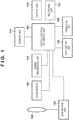
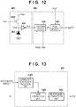
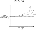
- Bildsensor mit einer Vielzahl von Pixeln, die jeweils aufweisen:eine Erfassungseinrichtung (301) zum Erfassen von Photonen, eine Zähleinrichtung (306) zum Zählen einer Anzahl der erfassten Photonen und zum Ausgeben eines gezählten Wertes, eine Speichereinrichtung (307) zum Halten des gezählten Wertes und um jedes Mal, wenn eine vorbestimmte Belichtungsperiode abläuft, den gezählten Wert, der in der Speichereinrichtung gehalten wird, als einen ersten Zählwert auszugeben, ohne den gezählten Wert zurückzusetzen, nachdem er ausgegeben wurde;wobei der Bildsensor ferner aufweist:eine erste temporäre Speichereinrichtung (2311) zum Speichern des ersten Zählwerts, wenn die vorbestimmte Belichtungszeit zum ersten Mal abgelaufen ist;eine zweite temporäre Speichereinrichtung (2312) zum Speichern des ersten Zählwerts, wenn die vorbestimmte Belichtungsperiode ein zweites Mal nach dem ersten Mal abgelaufen ist;eine Berechnungseinrichtung (207) zum Berechnen eines zweiten Zählwerts, der ein Zählwert pro Einheitszeit ist, basierend auf der Belichtungsperiode und basierend auf einem Differenzwert zwischen dem ersten Zählwert, der in der zweiten temporären Speichereinrichtung gespeichert ist, und dem ersten Zählwert, der in der ersten temporären Speichereinrichtung gespeichert ist; undeine Korrektureinrichtung (207) zum Erhalten eines Korrekturkoeffizienten basierend auf dem zweiten Zählwert und zum Korrigieren des Differenzwerts wegen einer Verschlechterung einer Bildqualität, die durch eine Differenz der empfangenen Lichtmenge pro Einheitszeit verursacht wird, unter Verwendung des Korrekturkoeffizienten,wobei die Korrektureinrichtung einen größeren Wert als den Korrekturkoeffizienten in einem Fall, in dem der zweite Zählwert ein erster Wert ist, als in einem Fall, in dem der zweite Zählwert ein zweiter Wert, der kleiner als der erste Wert ist, ist, erhält.
- Bildsensor nach Anspruch 1, der ferner für jeden der Pixel aufweist:eine Additionseinrichtung (2002) zum Addieren der Differenzwerte für eine vorbestimmte Anzahl von aufeinanderfolgenden Belichtungsperioden,wobei die Zähleinrichtung (306) konfiguriert ist, den gezählten Wert jedes Mal, wenn die vorbestimmte Anzahl von aufeinanderfolgenden Belichtungsperioden abläuft, zurückzusetzen.
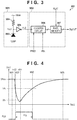
- Bildsensor nach einem der Ansprüche 1 bis 2, wobei die Erfassungseinrichtung (301) eine Lawinenfotodiode (303) und einen Quenchwiderstand (304) zum Anlegen einer Gegenspannung über die Lawinenfotodiode enthält.
- Bildsensor nach einem der Ansprüche 1 bis 2, wobei die Erfassungseinrichtung (301) eine Lawinenfotodiode (303) und einen MOS-Transistor (1201) zum Anlegen einer Gegenspannung über die Lawinenfotodiode enthält.
- Bildsensor nach einem der Ansprüche 1 bis 4, wobei der Bildsensor (100, 100') eine gestapelte Struktur hat, und die Erfassungseinrichtung (301) und die Zähleinrichtung (306) auf verschiedenen Substraten gebildet sind.
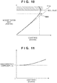
- Bildsensor nach einem der Ansprüche 1 bis 5, wobei der Korrekturkoeffizient ein Wert basierend auf einer Differenz zwischen dem zweiten Zählwert und einem Wert pro Einheitszeit eines idealen Zählwertes in einem Fall, in dem kein Erfassungsfehler auftritt, ist.
- Bildsensor nach einem der Ansprüche 1 bis 6, der ferner eine zweite Zähleinrichtung (1301), die Korrekturkoeffizienten entsprechend verschiedenen gezählten Werten pro Einheitszeit speichert, aufweist,
wobei die Korrektureinrichtung (1301) den Korrekturkoeffizienten entsprechend dem zweiten Zählwert von den Korrekturkoeffizienten, die in der zweiten Speichereinrichtung gespeichert sind, auswählt. - Bildsensor nach einem der Ansprüche 1 bis 6, wobei die Korrektureinrichtung (207) den Korrekturkoeffizienten entsprechend dem zweiten Zählwert unter Verwendung einer Approximationsfunktion zum Erhalten eines Korrekturkoeffizienten entsprechend dem gezählten Wert pro Einheitszeit erhält.
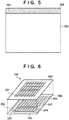
- Bildsensor nach einem der Ansprüche 1 bis 8, wobei ein Teil der Vielzahl der Pixel optisch schwarze Pixel (501, 201) sind, die vom Licht abgeschirmt sind, und
der Bildsensor (100, 100') ferner eine Schwarzniveaukorrektureinrichtung (803) zum Korrigieren des ersten Zählwerts, der von einem der Pixel (520, 201) ausgegeben wird, der nicht vom Licht abgeschirmt ist, und durch die Korrektureinrichtung mit einem zweiten Korrekturkoeffizienten zum Korrigieren eines Schwarzniveaus basierend auf dem zweiten Zählwert von dem einen der Pixel und einem Durchschnittswert der ersten Zählwerte, die von den optisch schwarzen Pixeln ausgegeben und durch die Korrektureinrichtung korrigiert wurden, enthält. - Bildsensor nach Anspruch 9, wobei die Schwarzniveaukorrektureinrichtung den zweiten Korrekturkoeffizienten basierend auf einem Durchschnitt der zweiten Zählwerte eines Pixels, der zu korrigieren ist, und seinen umgebenden Pixeln beschafft.
- Bildaufnahmevorrichtung, die aufweist:einen Bildsensor (100, 100') mit einer Vielzahl von Pixeln, die jeweils eine Erfassungseinrichtung (301) zum Erfassen von Photonen, eine Zähleinrichtung (306) zum Zählen einer Anzahl von erfassten Photonen und Ausgeben eines gezählten Wertes, eine Speichereinrichtung (307) zum Halten des gezählten Wertes und um jedes Mal, wenn eine vorbestimmte Belichtungsperiode abläuft, den gezählten Wert, der in der Speichereinrichtung gehalten wird, als einen ersten Zählwert auszugeben, ohne den gezählten Wert zurückzusetzen, nachdem er ausgegeben wurde, wobei die Bildaufnahmevorrichtung ferner aufweist:eine erste temporäre Speichereinrichtung (2311) zum Speichern des ersten Zählwerts, wenn die vorbestimmte Belichtungsperiode zum ersten Mal abgelaufen ist, und eine zweite temporäre Speichereinrichtung (2312) zum Speichern des ersten Zählwerts, wenn die vorbestimmte Belichtungsperiode zum zweiten Mal nach dem ersten Mal abgelaufen ist;eine Berechnungseinrichtung (207) zum Berechnen eines jeweiligen zweiten Zählwerts für jeden der Pixel, der ein Zählwert pro Einheitszeit ist, basierend auf der Belichtungsperiode und basierend auf einem jeweiligen Differenzwert zwischen dem ersten Zählwert, der in der jeweiligen zweiten temporären Speichereinrichtung gespeichert ist, und dem ersten Zählwert, der in der jeweiligen ersten temporären Speichereinrichtung gespeichert ist; undeine Korrektureinrichtung (207) zum Erhalten eines jeweiligen Korrekturkoeffizienten für jeden der Pixel basierend auf dem jeweiligen zweiten Zählwert und zum Korrigieren des jeweiligen Differenzwerts für jeden der Pixel wegen einer Verschlechterung einer Bildqualität, die durch eine Differenz der empfangenen Lichtmenge pro Einheitszeit verursacht wird, unter Verwendung des jeweiligen Korrekturkoeffizienten,wobei für jeden der Pixel die Korrektureinrichtung einen größeren Wert als den jeweiligen Korrekturkoeffizienten in einem Fall, in dem der jeweilige zweite Zählwert ein erster Wert ist, als in einem Fall, in dem der jeweilige zweite Zählwert ein zweiter Wert, der kleiner als der erste Wert ist, ist, erhält.
- Bildaufnahmevorrichtung nach Anspruch 11, wobei ein Teil der Vielzahl der Pixel optisch schwarze Pixel (501, 201) sind, die vom Licht abgeschirmt sind, und
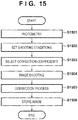
die Bildaufnahmevorrichtung ferner eine Schwarzniveaukorrektureinrichtung (803) zum Korrigieren des jeweiligen ersten Zählwerts, der von einem der Pixel (520, 201), der nicht vom Licht abgeschirmt ist, ausgegeben wird und der durch die Korrektureinrichtung um einen jeweiligen zweiten Korrekturkoeffizienten zum Korrigieren eines Schwarzniveaus basierend auf dem jeweiligen zweiten Zählwert des einen der Pixel und einem Durchschnittswert der ersten Zählwerte, die von den optisch schwarzen Pixeln ausgegeben werden und durch die Korrektureinrichtung korrigiert werden, aufweist. - Bildverarbeitungsverfahren, das aufweist:einen Berechnungsschritt des Berechnens eines zweiten Zählwerts, der ein Zählwert pro Einheitszeit ist, basierend auf einer vorbestimmten Belichtungsperiode und basierend auf einem Differenzwert zwischen ersten Zählwerten, die von einem Bildsensor (100, 100') ausgegeben und temporär gespeichert werden, wenn die vorbestimmte Belichtungsperiode zum ersten Mal und zum zweiten Mal nach dem ersten Mal abläuft, wobei der Bildsensor eine Vielzahl von Pixeln, die jeweils eine Erfassungseinrichtung (301) zum Erfassen von Photonen, eine Zähleinrichtung (306) zum Zählen einer Anzahl der erfassten Photonen und Ausgeben eines gezählten Wertes, und eine Speichereinrichtung (307) zum Halten des gezählten Wertes und um jedes Mal, wenn die vorbestimmte Belichtungsperiode abläuft, den gezählten Wert, der in der Speichereinrichtung gehalten wird, als einen ersten Zählwert auszugeben, ohne den gezählten Wert zurückzusetzen, nachdem er ausgegeben wurde, aufweist;einen Korrekturschritt des Erhaltens eines Korrekturkoeffizienten basierend auf einem zweiten Zählwert und des Korrigierens des Differenzwerts wegen einer Verschlechterung der Bildqualität, die durch eine Differenz des empfangenen Lichts pro Einheitszeit verursacht wird, unter Verwendung des Korrekturkoeffizienten,wobei in dem Korrekturschritt ein größerer Wert als der Korrekturkoeffizient in einem Fall, in dem der zweite Zählwert ein erster Wert ist, als in einem Fall, in dem der zweite Zählwert ein zweiter Wert, der kleiner als der erste Wert ist, ist, erhalten wird.
- Bildverarbeitungsverfahren nach Anspruch 13, wobei ein Teil der Vielzahl von Pixeln optisch schwarze Pixel (501, 201), die vom Licht abgeschirmt sind, sind, und
das Bildverarbeitungsverfahren ferner einen Schwarzniveaukorrekturschritt des Korrigierens des ersten Zählwerts, der von einem der Pixel (520, 201), der nicht vom Licht abgeschirmt ist und der durch die Korrektureinrichtung mit einem zweiten Korrekturkoeffizienten zum Korrigieren eines Schwarzniveaus basierend auf dem zweiten Zählwert des einen der Pixels und einem Durchschnittswert der ersten Zählwerte, die von den optisch schwarzen Pixeln ausgegeben werden und durch die Korrektureinrichtung korrigiert werden, aufweist. - Nicht flüchtiges Speichermedium, das durch einen Computer lesbar ist, wobei das Speichermedium ein Programm speichert, das durch einen Computer ausführbar ist, wobei das Programm einen Programmcode zum Veranlassen des Computers, das Bildverarbeitungsverfahren nach einem der Ansprüche 13 bis 14 auszuführen, enthält.
Applications Claiming Priority (1)
| Application Number | Priority Date | Filing Date | Title |
|---|---|---|---|
| JP2017241119A JP7062430B2 (ja) | 2017-12-15 | 2017-12-15 | 撮像素子、撮像装置および画像処理方法 |
Publications (3)
| Publication Number | Publication Date |
|---|---|
| EP3499873A2 EP3499873A2 (de) | 2019-06-19 |
| EP3499873A3 EP3499873A3 (de) | 2019-08-07 |
| EP3499873B1 true EP3499873B1 (de) | 2021-09-29 |
Family
ID=64664631
Family Applications (1)
| Application Number | Title | Priority Date | Filing Date |
|---|---|---|---|
| EP18211507.1A Active EP3499873B1 (de) | 2017-12-15 | 2018-12-11 | Korrektur für schwankungen in der empfangenen lichtmenge in einem photonenzählenden bildsensor |
Country Status (4)
| Country | Link |
|---|---|
| US (2) | US10785439B2 (de) |
| EP (1) | EP3499873B1 (de) |
| JP (1) | JP7062430B2 (de) |
| CN (1) | CN110022446B (de) |
Families Citing this family (16)
| Publication number | Priority date | Publication date | Assignee | Title |
|---|---|---|---|---|
| US11330202B2 (en) * | 2018-02-02 | 2022-05-10 | Sony Semiconductor Solutions Corporation | Solid-state image sensor, imaging device, and method of controlling solid-state image sensor |
| US11381806B2 (en) * | 2018-09-13 | 2022-07-05 | Pixart Imaging Inc. | Detection device and detection method using avalanche diode array and calibration matrix generating method thereof |
| US11039089B2 (en) * | 2019-03-27 | 2021-06-15 | Indian Institute Of Technology Ropar | Thermal imaging for identifying a defect in a material |
| KR20210000985A (ko) * | 2019-06-26 | 2021-01-06 | 삼성전자주식회사 | 비전 센서, 이를 포함하는 이미지 처리 장치 및 비전 센서의 동작 방법 |
| JP7292135B2 (ja) * | 2019-07-09 | 2023-06-16 | キヤノン株式会社 | 撮像素子及び撮像装置 |
| JP7393162B2 (ja) * | 2019-09-09 | 2023-12-06 | キヤノン株式会社 | 光電変換装置 |
| JP7427417B2 (ja) * | 2019-10-25 | 2024-02-05 | キヤノン株式会社 | 光電変換装置、光電変換システム、移動体、光電変換装置の検査方法 |
| KR20210054369A (ko) * | 2019-11-05 | 2021-05-13 | 삼성전자주식회사 | 센싱 모듈 및 이를 포함하는 생체 신호 측정 장치 |
| JP7444589B2 (ja) | 2019-12-03 | 2024-03-06 | キヤノン株式会社 | 撮像装置およびその制御方法 |
| CN111721411B (zh) * | 2020-06-30 | 2021-06-04 | 北京工业大学 | 一种用于高时空分辨光子计数成像的信号处理电路 |
| JP2022096472A (ja) * | 2020-12-17 | 2022-06-29 | キヤノン株式会社 | 光電変換装置及びその駆動方法 |
| KR20220095595A (ko) * | 2020-12-30 | 2022-07-07 | 에스케이하이닉스 주식회사 | 이미지 센서, 이를 이용한 이미지 센서 테스트 시스템 및 방법 |
| US11696049B2 (en) * | 2021-05-28 | 2023-07-04 | Microsoft Technology Licensing, Llc | Systems and methods for dark current compensation in single photon avalanche diode imagery |
| US11711628B2 (en) | 2021-05-28 | 2023-07-25 | Microsoft Technology Licensing, Llc | Systems and methods for obtaining color imagery using single photon avalanche diodes |
| US11765475B2 (en) * | 2021-10-20 | 2023-09-19 | Microsoft Technology Licensing, Llc | Systems and methods for obtaining dark current images |
| WO2023148148A1 (en) * | 2022-02-01 | 2023-08-10 | Sony Semiconductor Solutions Corporation | Imaging device and method |
Family Cites Families (26)
| Publication number | Priority date | Publication date | Assignee | Title |
|---|---|---|---|---|
| JPS5917160B2 (ja) | 1979-05-19 | 1984-04-19 | ライオン株式会社 | レコ−ド盤用清浄化剤 |
| US20030076431A1 (en) * | 2001-10-24 | 2003-04-24 | Krymski Alexander I. | Image sensor with pixels having multiple capacitive storage elements |
| DE10357187A1 (de) * | 2003-12-08 | 2005-06-30 | Siemens Ag | Verfahren zum Betrieb eines zählenden Strahlungsdetektors mit verbesserter Linearität |
| US20060124832A1 (en) | 2004-09-27 | 2006-06-15 | Lightspin Technologies, Inc. | Wide dynamic range photodetector |
| RU2411542C2 (ru) | 2005-04-22 | 2011-02-10 | Конинклейке Филипс Электроникс Н.В. | Цифровой кремниевый фотоумножитель для врп-пэт |
| JP5598905B2 (ja) | 2010-02-26 | 2014-10-01 | 独立行政法人日本原子力研究開発機構 | 中性子イメージ検出方法及びその方法を用いた中性子イメージ検出器 |
| JP5534997B2 (ja) * | 2010-08-03 | 2014-07-02 | 富士フイルム株式会社 | 電子内視鏡システム |
| JP5797884B2 (ja) | 2010-08-04 | 2015-10-21 | 株式会社日立ハイテクノロジーズ | 光量検出方法及びその装置 |
| US8716643B2 (en) | 2010-09-06 | 2014-05-06 | King Abdulaziz City Science And Technology | Single photon counting image sensor and method |
| WO2013003497A1 (en) * | 2011-06-28 | 2013-01-03 | Area Detector Systems Corporation | Dual mode pixel array detector |
| AU2012292250A1 (en) | 2011-07-20 | 2014-01-23 | Dectris Ltd. | Photon counting imaging method and device with instant retrigger capability |
| JP5676419B2 (ja) | 2011-11-24 | 2015-02-25 | 株式会社日立ハイテクノロジーズ | 欠陥検査方法およびその装置 |
| EP2790400A1 (de) * | 2011-12-09 | 2014-10-15 | Sony Corporation | Bildaufnahmevorrichtung, elektronische vorrichtung, optisch stimulierter lumineszenzerkennungsscanner und bildaufnahmeverfahren |
| JP5917160B2 (ja) | 2012-01-17 | 2016-05-11 | キヤノン株式会社 | 撮像装置、画像処理装置、画像処理方法およびプログラム |
| CN104170372B (zh) | 2012-02-27 | 2019-10-15 | 索尼半导体解决方案公司 | 成像元件和电子设备 |
| JP6017916B2 (ja) | 2012-10-16 | 2016-11-02 | 株式会社豊田中央研究所 | 光検出器 |
| KR20150099727A (ko) * | 2012-12-20 | 2015-09-01 | 소니 주식회사 | 촬상 소자, 촬상 장치, 전자 기기, 임계치 산출 장치 및 촬상 방법 |
| GB201300334D0 (en) * | 2013-01-09 | 2013-02-20 | St Microelectronics Ltd | Sensor circuit |
| US9596421B1 (en) | 2013-01-17 | 2017-03-14 | Princeton Lightwave, Inc. | Apparatus comprising a high dynamic range single-photon passive 2d imager and methods therefor |
| CN105188547B (zh) * | 2013-05-10 | 2019-06-04 | 皇家飞利浦有限公司 | 光子计数探测器校准 |
| JP2015109503A (ja) * | 2013-12-03 | 2015-06-11 | ソニー株式会社 | イメージセンサおよびイメージセンサの動作方法、撮像装置、電子機器、並びにプログラム |
| US9210350B2 (en) | 2013-12-09 | 2015-12-08 | Omnivision Technologies, Inc. | Low power imaging system with single photon avalanche diode photon counters and ghost image reduction |
| JP2016223952A (ja) * | 2015-06-01 | 2016-12-28 | キヤノン株式会社 | 放射線撮像装置、およびその制御方法 |
| JP6456854B2 (ja) | 2016-01-12 | 2019-01-23 | 株式会社日立製作所 | 放射線撮像装置 |
| CN105578082B (zh) * | 2016-01-29 | 2019-01-18 | 深圳市高巨创新科技开发有限公司 | 一种自适应黑电平校正方法 |
| CN107238854A (zh) * | 2017-07-25 | 2017-10-10 | 苏州瑞派宁科技有限公司 | 一种数字pet探测器的增益校正装置 |
-
2017
- 2017-12-15 JP JP2017241119A patent/JP7062430B2/ja active Active
-
2018
- 2018-12-11 US US16/215,789 patent/US10785439B2/en active Active
- 2018-12-11 EP EP18211507.1A patent/EP3499873B1/de active Active
- 2018-12-14 CN CN201811534272.4A patent/CN110022446B/zh active Active
-
2020
- 2020-07-15 US US16/929,259 patent/US11089256B2/en active Active
Also Published As
| Publication number | Publication date |
|---|---|
| CN110022446A (zh) | 2019-07-16 |
| JP2019110406A (ja) | 2019-07-04 |
| CN110022446B (zh) | 2022-08-12 |
| EP3499873A3 (de) | 2019-08-07 |
| JP7062430B2 (ja) | 2022-05-06 |
| US11089256B2 (en) | 2021-08-10 |
| EP3499873A2 (de) | 2019-06-19 |
| US10785439B2 (en) | 2020-09-22 |
| US20200351464A1 (en) | 2020-11-05 |
| US20190191120A1 (en) | 2019-06-20 |
Similar Documents
| Publication | Publication Date | Title |
|---|---|---|
| EP3499873B1 (de) | Korrektur für schwankungen in der empfangenen lichtmenge in einem photonenzählenden bildsensor | |
| US7999866B2 (en) | Imaging apparatus and processing method thereof | |
| US8908065B2 (en) | Solid state imaging processing systems and method for providing signal correction of pixel saturation errors | |
| JP5852324B2 (ja) | 撮像装置及びその制御方法、プログラム | |
| US9544512B2 (en) | Image capturing apparatus and method of reading out pixel signals from an image sensor | |
| US10771724B2 (en) | Image capturing apparatus | |
| US9118855B2 (en) | Solid-state imaging device, signal processing method thereof, and electronic apparatus | |
| US10638072B2 (en) | Control apparatus, image pickup apparatus, and control method for performing noise correction of imaging signal | |
| US10785423B2 (en) | Image sensor, image capturing apparatus, and image capturing method | |
| US20210274114A1 (en) | Image pickup apparatus, solid-state image pickup device, and control method for image pickup apparatus | |
| US10158813B2 (en) | Image pickup device, electronic apparatus, radiation detection apparatus and method for an image pickup device | |
| US10536675B2 (en) | Image capturing apparatus, driving method therefor, and image capturing system | |
| US10321075B2 (en) | Imaging apparatus and imaging system | |
| US20180027202A1 (en) | Image sensing device and control method thereof | |
| US10009559B2 (en) | Imaging apparatus, method for controlling the same, and program | |
| WO2010131533A1 (en) | Image capturing apparatus and control method for the same | |
| JP2019140464A (ja) | 撮像装置及び撮像方法 | |
| JP2020036066A (ja) | 撮像装置および制御方法 | |
| JP5737924B2 (ja) | 撮像装置 | |
| US11843890B2 (en) | Photoelectric conversion device, image pickup apparatus, control method, and storage medium | |
| US20240107199A1 (en) | Photoelectric conversion device, control method, and storage medium | |
| JP2011166234A (ja) | 固体撮像装置 | |
| JP2012129871A (ja) | 撮像装置 |
Legal Events
| Date | Code | Title | Description |
|---|---|---|---|
| PUAI | Public reference made under article 153(3) epc to a published international application that has entered the european phase |
Free format text: ORIGINAL CODE: 0009012 |
|
| STAA | Information on the status of an ep patent application or granted ep patent |
Free format text: STATUS: THE APPLICATION HAS BEEN PUBLISHED |
|
| AK | Designated contracting states |
Kind code of ref document: A2 Designated state(s): AL AT BE BG CH CY CZ DE DK EE ES FI FR GB GR HR HU IE IS IT LI LT LU LV MC MK MT NL NO PL PT RO RS SE SI SK SM TR |
|
| AX | Request for extension of the european patent |
Extension state: BA ME |
|
| PUAL | Search report despatched |
Free format text: ORIGINAL CODE: 0009013 |
|
| AK | Designated contracting states |
Kind code of ref document: A3 Designated state(s): AL AT BE BG CH CY CZ DE DK EE ES FI FR GB GR HR HU IE IS IT LI LT LU LV MC MK MT NL NO PL PT RO RS SE SI SK SM TR |
|
| AX | Request for extension of the european patent |
Extension state: BA ME |
|
| RIC1 | Information provided on ipc code assigned before grant |
Ipc: H04N 5/3745 20110101AFI20190704BHEP Ipc: H01L 31/107 20060101ALI20190704BHEP Ipc: G01T 1/24 20060101ALI20190704BHEP Ipc: G01J 1/44 20060101ALI20190704BHEP Ipc: H01L 27/146 20060101ALI20190704BHEP Ipc: H04N 5/369 20110101ALI20190704BHEP |
|
| STAA | Information on the status of an ep patent application or granted ep patent |
Free format text: STATUS: REQUEST FOR EXAMINATION WAS MADE |
|
| 17P | Request for examination filed |
Effective date: 20200207 |
|
| RBV | Designated contracting states (corrected) |
Designated state(s): AL AT BE BG CH CY CZ DE DK EE ES FI FR GB GR HR HU IE IS IT LI LT LU LV MC MK MT NL NO PL PT RO RS SE SI SK SM TR |
|
| STAA | Information on the status of an ep patent application or granted ep patent |
Free format text: STATUS: EXAMINATION IS IN PROGRESS |
|
| 17Q | First examination report despatched |
Effective date: 20200720 |
|
| STAA | Information on the status of an ep patent application or granted ep patent |
Free format text: STATUS: EXAMINATION IS IN PROGRESS |
|
| GRAP | Despatch of communication of intention to grant a patent |
Free format text: ORIGINAL CODE: EPIDOSNIGR1 |
|
| STAA | Information on the status of an ep patent application or granted ep patent |
Free format text: STATUS: GRANT OF PATENT IS INTENDED |
|
| INTG | Intention to grant announced |
Effective date: 20210415 |
|
| RIN1 | Information on inventor provided before grant (corrected) |
Inventor name: IKEDO, HIDEKI |
|
| GRAS | Grant fee paid |
Free format text: ORIGINAL CODE: EPIDOSNIGR3 |
|
| GRAA | (expected) grant |
Free format text: ORIGINAL CODE: 0009210 |
|
| STAA | Information on the status of an ep patent application or granted ep patent |
Free format text: STATUS: THE PATENT HAS BEEN GRANTED |
|
| AK | Designated contracting states |
Kind code of ref document: B1 Designated state(s): AL AT BE BG CH CY CZ DE DK EE ES FI FR GB GR HR HU IE IS IT LI LT LU LV MC MK MT NL NO PL PT RO RS SE SI SK SM TR |
|
| REG | Reference to a national code |
Ref country code: GB Ref legal event code: FG4D |
|
| REG | Reference to a national code |
Ref country code: DE Ref legal event code: R096 Ref document number: 602018024215 Country of ref document: DE |
|
| REG | Reference to a national code |
Ref country code: CH Ref legal event code: EP Ref country code: AT Ref legal event code: REF Ref document number: 1435275 Country of ref document: AT Kind code of ref document: T Effective date: 20211015 |
|
| REG | Reference to a national code |
Ref country code: IE Ref legal event code: FG4D |
|
| REG | Reference to a national code |
Ref country code: LT Ref legal event code: MG9D |
|
| PG25 | Lapsed in a contracting state [announced via postgrant information from national office to epo] |
Ref country code: HR Free format text: LAPSE BECAUSE OF FAILURE TO SUBMIT A TRANSLATION OF THE DESCRIPTION OR TO PAY THE FEE WITHIN THE PRESCRIBED TIME-LIMIT Effective date: 20210929 Ref country code: FI Free format text: LAPSE BECAUSE OF FAILURE TO SUBMIT A TRANSLATION OF THE DESCRIPTION OR TO PAY THE FEE WITHIN THE PRESCRIBED TIME-LIMIT Effective date: 20210929 Ref country code: SE Free format text: LAPSE BECAUSE OF FAILURE TO SUBMIT A TRANSLATION OF THE DESCRIPTION OR TO PAY THE FEE WITHIN THE PRESCRIBED TIME-LIMIT Effective date: 20210929 Ref country code: RS Free format text: LAPSE BECAUSE OF FAILURE TO SUBMIT A TRANSLATION OF THE DESCRIPTION OR TO PAY THE FEE WITHIN THE PRESCRIBED TIME-LIMIT Effective date: 20210929 Ref country code: NO Free format text: LAPSE BECAUSE OF FAILURE TO SUBMIT A TRANSLATION OF THE DESCRIPTION OR TO PAY THE FEE WITHIN THE PRESCRIBED TIME-LIMIT Effective date: 20211229 Ref country code: BG Free format text: LAPSE BECAUSE OF FAILURE TO SUBMIT A TRANSLATION OF THE DESCRIPTION OR TO PAY THE FEE WITHIN THE PRESCRIBED TIME-LIMIT Effective date: 20211229 Ref country code: LT Free format text: LAPSE BECAUSE OF FAILURE TO SUBMIT A TRANSLATION OF THE DESCRIPTION OR TO PAY THE FEE WITHIN THE PRESCRIBED TIME-LIMIT Effective date: 20210929 |
|
| REG | Reference to a national code |
Ref country code: NL Ref legal event code: MP Effective date: 20210929 |
|
| REG | Reference to a national code |
Ref country code: AT Ref legal event code: MK05 Ref document number: 1435275 Country of ref document: AT Kind code of ref document: T Effective date: 20210929 |
|
| PG25 | Lapsed in a contracting state [announced via postgrant information from national office to epo] |
Ref country code: LV Free format text: LAPSE BECAUSE OF FAILURE TO SUBMIT A TRANSLATION OF THE DESCRIPTION OR TO PAY THE FEE WITHIN THE PRESCRIBED TIME-LIMIT Effective date: 20210929 Ref country code: GR Free format text: LAPSE BECAUSE OF FAILURE TO SUBMIT A TRANSLATION OF THE DESCRIPTION OR TO PAY THE FEE WITHIN THE PRESCRIBED TIME-LIMIT Effective date: 20211230 |
|
| PG25 | Lapsed in a contracting state [announced via postgrant information from national office to epo] |
Ref country code: AT Free format text: LAPSE BECAUSE OF FAILURE TO SUBMIT A TRANSLATION OF THE DESCRIPTION OR TO PAY THE FEE WITHIN THE PRESCRIBED TIME-LIMIT Effective date: 20210929 |
|
| PG25 | Lapsed in a contracting state [announced via postgrant information from national office to epo] |
Ref country code: IS Free format text: LAPSE BECAUSE OF FAILURE TO SUBMIT A TRANSLATION OF THE DESCRIPTION OR TO PAY THE FEE WITHIN THE PRESCRIBED TIME-LIMIT Effective date: 20220129 Ref country code: SK Free format text: LAPSE BECAUSE OF FAILURE TO SUBMIT A TRANSLATION OF THE DESCRIPTION OR TO PAY THE FEE WITHIN THE PRESCRIBED TIME-LIMIT Effective date: 20210929 Ref country code: RO Free format text: LAPSE BECAUSE OF FAILURE TO SUBMIT A TRANSLATION OF THE DESCRIPTION OR TO PAY THE FEE WITHIN THE PRESCRIBED TIME-LIMIT Effective date: 20210929 Ref country code: PT Free format text: LAPSE BECAUSE OF FAILURE TO SUBMIT A TRANSLATION OF THE DESCRIPTION OR TO PAY THE FEE WITHIN THE PRESCRIBED TIME-LIMIT Effective date: 20220131 Ref country code: PL Free format text: LAPSE BECAUSE OF FAILURE TO SUBMIT A TRANSLATION OF THE DESCRIPTION OR TO PAY THE FEE WITHIN THE PRESCRIBED TIME-LIMIT Effective date: 20210929 Ref country code: NL Free format text: LAPSE BECAUSE OF FAILURE TO SUBMIT A TRANSLATION OF THE DESCRIPTION OR TO PAY THE FEE WITHIN THE PRESCRIBED TIME-LIMIT Effective date: 20210929 Ref country code: ES Free format text: LAPSE BECAUSE OF FAILURE TO SUBMIT A TRANSLATION OF THE DESCRIPTION OR TO PAY THE FEE WITHIN THE PRESCRIBED TIME-LIMIT Effective date: 20210929 Ref country code: EE Free format text: LAPSE BECAUSE OF FAILURE TO SUBMIT A TRANSLATION OF THE DESCRIPTION OR TO PAY THE FEE WITHIN THE PRESCRIBED TIME-LIMIT Effective date: 20210929 Ref country code: CZ Free format text: LAPSE BECAUSE OF FAILURE TO SUBMIT A TRANSLATION OF THE DESCRIPTION OR TO PAY THE FEE WITHIN THE PRESCRIBED TIME-LIMIT Effective date: 20210929 Ref country code: AL Free format text: LAPSE BECAUSE OF FAILURE TO SUBMIT A TRANSLATION OF THE DESCRIPTION OR TO PAY THE FEE WITHIN THE PRESCRIBED TIME-LIMIT Effective date: 20210929 |
|
| REG | Reference to a national code |
Ref country code: DE Ref legal event code: R097 Ref document number: 602018024215 Country of ref document: DE |
|
| REG | Reference to a national code |
Ref country code: DE Ref legal event code: R119 Ref document number: 602018024215 Country of ref document: DE |
|
| PG25 | Lapsed in a contracting state [announced via postgrant information from national office to epo] |
Ref country code: MC Free format text: LAPSE BECAUSE OF FAILURE TO SUBMIT A TRANSLATION OF THE DESCRIPTION OR TO PAY THE FEE WITHIN THE PRESCRIBED TIME-LIMIT Effective date: 20210929 Ref country code: DK Free format text: LAPSE BECAUSE OF FAILURE TO SUBMIT A TRANSLATION OF THE DESCRIPTION OR TO PAY THE FEE WITHIN THE PRESCRIBED TIME-LIMIT Effective date: 20210929 |
|
| REG | Reference to a national code |
Ref country code: CH Ref legal event code: PL |
|
| PLBE | No opposition filed within time limit |
Free format text: ORIGINAL CODE: 0009261 |
|
| STAA | Information on the status of an ep patent application or granted ep patent |
Free format text: STATUS: NO OPPOSITION FILED WITHIN TIME LIMIT |
|
| 26N | No opposition filed |
Effective date: 20220630 |
|
| REG | Reference to a national code |
Ref country code: BE Ref legal event code: MM Effective date: 20211231 |
|
| PG25 | Lapsed in a contracting state [announced via postgrant information from national office to epo] |
Ref country code: LU Free format text: LAPSE BECAUSE OF NON-PAYMENT OF DUE FEES Effective date: 20211211 Ref country code: IE Free format text: LAPSE BECAUSE OF NON-PAYMENT OF DUE FEES Effective date: 20211211 Ref country code: DE Free format text: LAPSE BECAUSE OF NON-PAYMENT OF DUE FEES Effective date: 20220701 |
|
| PG25 | Lapsed in a contracting state [announced via postgrant information from national office to epo] |
Ref country code: SI Free format text: LAPSE BECAUSE OF FAILURE TO SUBMIT A TRANSLATION OF THE DESCRIPTION OR TO PAY THE FEE WITHIN THE PRESCRIBED TIME-LIMIT Effective date: 20210929 Ref country code: FR Free format text: LAPSE BECAUSE OF NON-PAYMENT OF DUE FEES Effective date: 20211231 Ref country code: BE Free format text: LAPSE BECAUSE OF NON-PAYMENT OF DUE FEES Effective date: 20211231 |
|
| PG25 | Lapsed in a contracting state [announced via postgrant information from national office to epo] |
Ref country code: LI Free format text: LAPSE BECAUSE OF NON-PAYMENT OF DUE FEES Effective date: 20211231 Ref country code: CH Free format text: LAPSE BECAUSE OF NON-PAYMENT OF DUE FEES Effective date: 20211231 |
|
| PG25 | Lapsed in a contracting state [announced via postgrant information from national office to epo] |
Ref country code: IT Free format text: LAPSE BECAUSE OF FAILURE TO SUBMIT A TRANSLATION OF THE DESCRIPTION OR TO PAY THE FEE WITHIN THE PRESCRIBED TIME-LIMIT Effective date: 20210929 |
|
| PG25 | Lapsed in a contracting state [announced via postgrant information from national office to epo] |
Ref country code: CY Free format text: LAPSE BECAUSE OF FAILURE TO SUBMIT A TRANSLATION OF THE DESCRIPTION OR TO PAY THE FEE WITHIN THE PRESCRIBED TIME-LIMIT Effective date: 20210929 |
|
| PG25 | Lapsed in a contracting state [announced via postgrant information from national office to epo] |
Ref country code: SM Free format text: LAPSE BECAUSE OF FAILURE TO SUBMIT A TRANSLATION OF THE DESCRIPTION OR TO PAY THE FEE WITHIN THE PRESCRIBED TIME-LIMIT Effective date: 20210929 Ref country code: HU Free format text: LAPSE BECAUSE OF FAILURE TO SUBMIT A TRANSLATION OF THE DESCRIPTION OR TO PAY THE FEE WITHIN THE PRESCRIBED TIME-LIMIT; INVALID AB INITIO Effective date: 20181211 |
|
| PGFP | Annual fee paid to national office [announced via postgrant information from national office to epo] |
Ref country code: GB Payment date: 20231121 Year of fee payment: 6 |
|
| PG25 | Lapsed in a contracting state [announced via postgrant information from national office to epo] |
Ref country code: MK Free format text: LAPSE BECAUSE OF FAILURE TO SUBMIT A TRANSLATION OF THE DESCRIPTION OR TO PAY THE FEE WITHIN THE PRESCRIBED TIME-LIMIT Effective date: 20210929 |