EP0745235B1 - Photomask blanks - Google Patents
Photomask blanks Download PDFInfo
- Publication number
- EP0745235B1 EP0745235B1 EP95908787A EP95908787A EP0745235B1 EP 0745235 B1 EP0745235 B1 EP 0745235B1 EP 95908787 A EP95908787 A EP 95908787A EP 95908787 A EP95908787 A EP 95908787A EP 0745235 B1 EP0745235 B1 EP 0745235B1
- Authority
- EP
- European Patent Office
- Prior art keywords
- film
- photomask blank
- eps
- wavelength
- phase shifter
- Prior art date
- Legal status (The legal status is an assumption and is not a legal conclusion. Google has not performed a legal analysis and makes no representation as to the accuracy of the status listed.)
- Expired - Lifetime
Links
Images


Classifications
-
- G—PHYSICS
- G03—PHOTOGRAPHY; CINEMATOGRAPHY; ANALOGOUS TECHNIQUES USING WAVES OTHER THAN OPTICAL WAVES; ELECTROGRAPHY; HOLOGRAPHY
- G03F—PHOTOMECHANICAL PRODUCTION OF TEXTURED OR PATTERNED SURFACES, e.g. FOR PRINTING, FOR PROCESSING OF SEMICONDUCTOR DEVICES; MATERIALS THEREFOR; ORIGINALS THEREFOR; APPARATUS SPECIALLY ADAPTED THEREFOR
- G03F1/00—Originals for photomechanical production of textured or patterned surfaces, e.g., masks, photo-masks, reticles; Mask blanks or pellicles therefor; Containers specially adapted therefor; Preparation thereof
- G03F1/26—Phase shift masks [PSM]; PSM blanks; Preparation thereof
- G03F1/32—Attenuating PSM [att-PSM], e.g. halftone PSM or PSM having semi-transparent phase shift portion; Preparation thereof
Definitions
- This invention relates to photomask blanks, and more particularly, to photomask blanks providing phase shift in incident light at a specified wavelength.
- Photomask blanks commonly consist of a substrate, e.g., fused silica plate, on which is an opaque chrome film. Photomasks are produced from these blanks by providing a desired pattern of open areas in the film. In use, light is optically projected through the open areas of the photomask onto the surface of a light sensitive substrate, such as a photopolymer-coated semiconductor wafer.
- a light sensitive substrate such as a photopolymer-coated semiconductor wafer.
- photomasks are illuminated with visible or ultraviolet light.
- a fundamental limitation of optical imaging is that line widths of the order of the wavelength of the illuminating light are diffraction limited. In other words, light having a wavelength of the same order of magnitude as the desired optical image will diffract, and the projected image will be wider than the desired image.
- U.S. Patent No. 4,890,309 discloses a type of attenuated (as opposed to opaque) photomask, particularly useful in X-ray lithography, wherein the material and thickness of the attenuating film are selected to both pass (i.e., transmit) a fraction of the incident electromagnetic radiation and to phase shift the radiation relative to radiation passing through the open features of the mask.
- the materials of choice are homogeneous films of tungsten, gold, silver, alloys of these materials or alternating layers of high and low atomic number materials (e.g., tungsten and carbon).
- phase-shifting photomasks In an effort to avoid the cost and complexity of X-ray lithography, a variety of phase-shifting photomasks have been developed for ultraviolet and visible light ranges (see, for example, B. J. Lin, Solid State Technology, pp. 43-47, January, 1992). Among these are the rim phase-shifting photomask, which requires either substrate etching or the use of an additional phase-shifting layer. The rim phase-shifting photomask is inherently applicable to arbitrary mask patterns, but requires a large positive mask bias to reduce exposure times to a practical level and due to strong proximity effects it is difficult to delineate all feature sizes and shapes for an arbitrary mask pattern using one common exposure.
- APSPM attenuated phase-shifting photomask
- APSPMs employ an absorptive, partially transmitting, phase shifter in place of the conventional opaque chromium part of the patterned film.
- the transmission of the absorptive phase shifter is adjusted to less than about 0.20 to prevent creation of ghost lines.
- not all phase shifters can phase shift and absorb by the desired amount. Consequently, a multilayered structure consisting of materials of differing absorptive and phase shifting properties may be required in some cases.
- a commercially available APSPM utilizes a graded chromium oxycarbonitride composition film which varies from a Cr-N compound at the substrate-film interface to a Cr-O compound at the film-air interface, which also serves as an anti-reflective coating. While this APSPM provides a degree of phase shifting, a further procedure, such as reactive ion etching of the substrate, in this case, fused silica, is necessary to achieve the desired 180° phase shift.
- Japanese laid-open patent application No. Heisei 5-127,361 describes an attenuating photomask blank with a partially transmitting film that provides both the desired transmission and phase shift, i.e., the phase shift is embedded in the absorbing layer.
- This is achieved by the use of a depthwise optically homogeneous film material with appropriate index of refraction and extinction coefficient.
- a disadvantage of this depthwise homogeneous film is that, because the index of refraction and extinction coefficient are coupled, the transmission, phase shift, and reflectivity cannot be separately selected. In general, lithographic imaging performance is affected by transmission, phase shift, and reflectivity, so independent control of these three parameters is desirable.
- Another disadvantage of this homogeneous film is that when chromium compounds are used as specified in the claims, the electrical resistivity is high, rendering the film unwritable in an electron beam patterning system unless a separate charge dissipation layer is used.
- a further disadvantage of this homogeneous film is that when chromium compounds are used, the spectral optical transmission is very high in the visible portion of the spectrum, causing difficulty in inspecting the finished photomask (customarily done at 488 nm) and aligning the finished photomask in the projection aligner (customarily done at 633 nm).
- the inhomogeneous attenuating film consists essentially of a combination of a metallic component and a dielectric component, wherein one surface of the film has a higher content of metallic component than the other surface, and the profile of change in the extinction coefficient is gradual through the film thickness; and wherein said profile of change and the film thickness are selected to provide a phase shift of about 180° (or an odd multiple thereof) at the selected wavelength.
- This inhomogeneous film allows flexible design and construction of photomask blanks with independent control of transmission, phase shift, and reflectivity. However, it specifies a depthwise composition gradient between a metallic component and a dielectric component.
- WO-A-9411786 which was published on 26th May 1994 and forms part of the state of the art by virtue of Article 54 (3) EPC in respect of the designations of France, Germany, The Netherlands and The United Kingdom, describes a transmissive embedded phase shifter-photomask blank which comprises an optically inhomogeneous attenuating film which has a transmission of at least 0.001 and consists essentially of a combination of a metallic component and a dielectric component.
- One surface of the film has a higher content of metallic component than the other surface, and the profile of change in extinction coefficient is gradual through the film thickness.
- the profile of change in extinction coefficient and the film thickness are selected to provide a phase shift of about 180°, or an odd multiple thereof, at a selected wavelength.
- transmissive embedded phase shifter-photomask blank as defined in Claim 1.
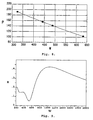
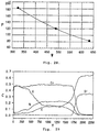
- Figure 1 represents a compositional depth profile of a EPS-PMB provided in accordance with this invention having a .054 transmission at 365 nm wavelength.
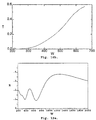
- Figure 2 represents spectral transmission of the EPS-PMB of Figure 1.
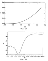
- Figures 3a and 3b represent ellipsometric data for Psi and Delta, respectively, in degrees, for the EPS-PMB of Figure 1.
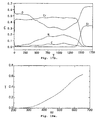
- Figures 4a and 4b represent effective optical constants (n and k) for the more absorbing and less absorbing components, respectively, for the EPS-PMB of Figure 1.
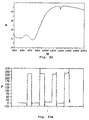
- Figure 5 represents a depth profile of effective optical constants (n and k) for the EPS-PMB of Figure 1.
- Figure 6 represents an ellipsometrically modeled spectral phase shifts for the EPS-PMB of Figure 1.
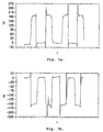
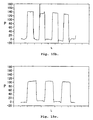
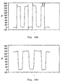
- Figures 7a, 7b, 7c and 7d represent phase sensitive interferometer scans at 325, 442, 488 and 633 nm, respectively, for the EPS-PMB of Figure 1.
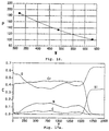
- Figure 8 represents a plot of 325, 442, 488, and 633 nm PSI data for the EPS-PMB of Figure 1 along with a second-order curve fit to the data (the interpolated I-line phase shift is 179° for this EPS-PMB).
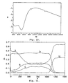
- Figure 9 represents the reflectance for light incident on the film side of the EPS-PMB of Figure 1.
- Figure 10 represents the reflectance for light incident on the substrate side of the EPS-PMB of Figure 1.
- Figure 11 represents a compositional depth profile of another EPS-PMB provided in accordance with this invention with a chrome chemistry suitable for providing a 6.1% (i.e., 0.061) transmission at 365 nm wavelength, which has an optimized chrome chemistry, with increased carbon, for improved conductivity, and wet etch performance.
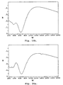
- Figure 12 represents spectral transmission of the EPS-PMB of Figure 11.
- Figure 13 represents the reflectance for light incident on the film side of the EPS-PMB of Figure 11.
- Figure 14 represents the reflectance for light incident on the substrate side of the EPS-PMB of Figure 11.
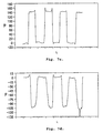
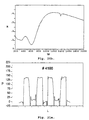
- Figures 15a, 15b and 15c represent phase sensitive interferometer scans at 325, 488, and 633 nm, respectively, for the EPS-PMB of Figure 11.
- Figure 16 represents a plot of 325, 488, and 633 nm PSI data for the EPS-PMB of Figure 11, along with a second-order curve fit to the data (the predicted I-line phase shift is 173° for this EPS-PMB).
- Figures 17a and 17b represent compositional depth profiles for two other photomask blanks, the photomask blank of 17a having the more absorbing component in the middle of the film, and the photomask of 17b having the more absorbing component at the base of the film.
- Figures 18a and 18b represent spectral transmission of the photomask blanks of Figures 17a and 17b, respectively.
- Figures 19a and 19b represent the reflectance for light incident on the film side of the photomask blanks of Figures 17a and 17b, respectively.
- Figures 20a and 20b represent reflectance for light incident on the substrate side of the photomask blanks of Figures 17a and 17b, respectively.
- Figures 21a, 21b, 21c, 21d, 21e, and 21f represent the phase sensitive interferometer scans for the photomask blanks of Figures 17a and 17b at 325 nm, 488 nm, and 633 nm, respectively.
- Figures 22a and 22b represent a plot of 325, 488, and 633 nm PSI data for the photomask blank of Figures 17a and 17b, respectively, along with a second-order curve fit to the data (the predicted I-line phase shift is 203° and 204°, respectively, for these photomask blanks).
- Figure 23 represents a compositional depth profile for another photomask blank with a chrome chemistry suitable for a 2.3% transmission at 248 nm (DUV).
- Figure 24 represents the transmission of the photomask blank of Figure 23.
- Figure 25 represents the reflectance for light incident on the film side of the photomask blank of Figure 23.
- Figure 26 represents the reflectance for light incident on the substrate side of the photomask blank of Figure 23.
- Figures 27a, 27b and 27c represent phase sensitive interferometer scans at 325, 488, and 633 nm, respectively, for the photomask blank of Figure 23.
- Figure 28 represents a plot of 325, 488, and 633 nm PSI data for the photomask blank of Figure 23 along with a second-order curve fit to the data (the predicted DUV phase shift is 219° for this photomask blank).
- Figure 29 represents a compositional depth profile of another EPS-PMB provided in accordance with this invention with a chrome chemistry suitable for providing a 6.3% G-line Transmission.
- Figure 30 represents a spectral transmission of the EPS-PMB of Figure 29.
- Figure 31 represents the reflectance for light incident on the film side of the EPS-PMB of Figure 29.
- Figure 32 represents the reflectance for light incident on the substrate side of the EPS-PMB of Figure 29.
- Figures 33a, 33b and 33c represent phase sensitive interferometer scans at 325, 488, and 633 nm, respectively, for the EPS-PMB of Figure 29.
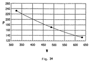
- Figure 34 represents a plot of 325, 488, and 633 nm PSI data for the EPS-PMB of Figure 29 along with a second-order curve fit to the data (the predicted G-line phase shift is 188° for this EPS-PMB).
- This invention provides an advantageous film for photomask blanks.
- the film provides a phase shift of about 180° (preferably 180° ⁇ 10°) or an odd multiple thereof, for particular incident wavelengths, and is thus especially useful for producing photomasks.
- the film is deposited on a substrate.
- the substrate can be any mechanically stable material which is transparent to the wavelength of incident light used. Substrates such as quartz and fused silica (glass) are preferred for availability and cost.
- the films of this invention are optically inhomogeneous, in that the refractive index and/or extinction coefficient change(s) through the film thickness.
- the optically inhomogeneous attenuating film in accordance with the instant invention is typically in the form of a continuously varying structure ranging from optically more absorbing characteristics at the lower surface (normally a substrate-film interface) to optically less absorbing characteristics at the upper surface (normally a film-air interface); or in the form of a continuously varying structure ranging from optically less absorbing characteristics at the lower surface (normally a substrate-film interface) to optically more absorbing characteristics at a location partially through the film thickness to optically less absorbing characteristics at the upper surface (normally a film-air interface); or in the form of a continually varying structure ranging from optically more absorbing characteristics at the lower surface (normally a substrate-film interface) to optically less absorbing characteristics at a location partially through the film thickness to optically more absorbing characteristics at the upper surface (normally a film-air
- the material can be defined to be a mixture of at least two components, at least one more absorbing component and at least one less absorbing component.
- the index of refraction of the more absorbing component(s) is generally from 1 to 6, and is preferably from 2 to 5; and the index of refraction of the less absorbing component(s) is generally from 1 to 3.5, and is preferably from 1.2 to 2.8.
- the extinction coefficient of the more absorbing component(s) is generally from 0 to 6 and is preferably from 0.5 to 3.5.
- the extinction coefficient of the less absorbing component(s) is generally from 0 to 2 and is preferably from 0 to 1.5.
- the more absorbing and less absorbing components of the inhomogeneous attenuating film can be selected from materials such as transition, and non-transition, metal fluoro-oxy-carbo-nitrides.
- Materials which are particularly suited to the practice of this invention are metal oxy-carbo-nitrides (i.e., M-O-C-N), metal chloro-oxy-carbo-nitrides (i.e., M-Cl-O-C-N), metal chloro-fluoro-oxy-carbo-nitrides (i.e., M-Cl-F-O-C-N) and metal fluoro-oxy-carbo-nitrides (i.e., M-F-O-C-N) where M is selected from the group consisting of Cr, Fe, Mo, Zn, Co, Nb, Ta, W, Ti, Al, Mg, Si, and mixtures thereof. Cr is a preferred M; and chromium oxy-carbonitride
- the profile of the film's refractive index, the profile of the film's extinction coefficients or both profiles change gradually through the film thickness.
- the gradual change can be accomplished in a smooth continuous manner and/or in a stepwise graded manner.
- the films of this invention are multicomponent compositions, wherein one component has a higher absorbancy than another component at the lithographic wavelength.
- the film composition is essentially a combination of two components.
- These two components may be a metallic component (i.e., a material characterized by an extinction coefficient within the range of 0 to 6 which generally decreases in magnitude with increasing photon energy in the range from 1.5 to 6.5 eV) and a dielectric component (i.e., a material characterized by an extinction coefficient within the range of 0 to 2 which generally increases in magnitude with increasing photon energy in the range from 1.5 to 6.5 eV) combined so that the profile of change in the extinction coefficient and the film thickness provide a phase shift of about 180° (or an odd multiple thereof) as in copending U.S. Patent Application Serial No. 07/976,782 (now US-A-5459002); or the two components may be another combination in accordance with this invention.
- a metallic component i.e., a material characterized by an extinction coefficient within the range of 0 to 6 which generally decreases in magnitude with increasing photon energy in the range from 1.5 to 6.5 eV
- a dielectric component i.e., a material characterized
- two dielectric materials i.e., two materials characterized by an extinction coefficient which generally increases with increasing photon energy within the range of 1.5 to 6.5 eV
- the use of two dielectric material facilitates achieving transmissions at I-line and G-line lithographic wavelengths of about 0.04 and above (e.g., between 0.04 and 0.50); and transmissions at DUV lithographic wavelengths of about 0.01 and above (e.g., between 0.01 and 0.12).
- the optically inhomogeneous film must have a degree of transparency sufficient for the phase shift provided by the film to have the desired effect on the line width produced by the photomask.
- m is typically equal to 1 or 3, but it is not limited to such, for example, in the X-ray region.
- the volumes of the more absorbing and less absorbing components can vary in thickness from essentially 0 to a thickness defined by the requirement that these inhomogeneous attenuating films have sufficient transparency.
- the more absorbing component is from 5 nanometers to 150 nanometers thick, and the less absorbing component is from 10 nanometers to 400 nanometers thick.
- composition of the film can be designed in accordance with multiple requirements that the film have the 180° phase shift required by embedded phase shifters at the desired wavelength of light employed, that the film have the desired transmission at the wavelength of light employed, and that the film have the desired reflectance at the wavelength of light employed.
- EPS-PMBs where the lithographic wavelength is I-line
- EPS-PMBs in accordance with this invention where the lithographic wavelength is DUV
- EPS-PMBs in accordance with this invention wherein the lithographic wavelength is G-line.
- desired reflectances are within the range of from 0 to about 0.5.
- a generalized design may be constructed with the more absorbing component at one film surface (e.g., adjacent to the substrate), and the less absorbing component at the other film surface (e.g., adjacent to air) and a selected profile of gradual transition from more absorbing to less absorbing as discussed above.
- the index of refraction and extinction coefficient for each of the two components along with an estimated film thickness and a selected profile of change in optical properties, one may calculate the transmission, reflectivity, and phase shift for the film.
- One may use the well known matrix method (see O. S. Heavens, "Optical Properties of Thin Solid Films", Dover Publications, NY, 1965, pp.
- Computers may be used to perform the numerical computations. For a given profile, optimization of the film design is accomplished by calculating transmission, reflectivity and phase shift combinations within manufacturable ranges, and determining which combinations provide the preferred solutions. Using computerized calculations based upon the matrix method, the profile may be modeled as a large number of thin homogeneous layers, and the characteristic matrices of all the layers are matrix multiplied to calculate the reflectivity, transmission and phase shift for the film. Predetermined optical property profiles might be used, such as linear, quadratic, cubic, exponential or gaussian. In practice the profile will be constrained by the particular equipment used to manufacture the films. The equipment will also normally determine the upper and lower limits for thicknesses of regions in the film structure.
- the spectral optical characteristics of the inhomogeneous film can be tuned to accommodate the requirements of photomask inspection and alignment tools.
- these tools operate in the visible wavelength range and require low transmission (e.g., less than 0.60) at inspection and alignment wavelength(s) (typically 488 nm and 633 nm, respectively) to operate properly.
- the inhomogeneous film's composition profile can be adjusted so that the more absorbing component is concentrated in a relatively thin layer and provides the desired relatively flat spectral transmission response, while the layer(s) having higher concentration of the less absorbing component is thicker and provides the balance of the phase shift.
- the oxygen-deficient component may be concentrated in the relatively thin layer to facilitate alignment and inspection.
- composition profile of the inhomogeneous film can be adjusted as described above for flat spectral transmission response, so that the thin more absorbing component constitutes an electrically conductive layer consistent with the requirements of electron beam exposure.
- the carbon content can be increased to decrease the sheet resistance.
- Electron beam writing systems require an electrically conductive layer to facilitate charge dissipation. Films having sheet resistance of about 1 x 10 9 ohms/sq. or less (e.g., from 1 x 10 2 to 1 x 10 9 ohms/sq.) can be readily provided in accordance with this invention for I-line and G-line lithography.
- wet etching characteristics of the inhomogeneous film can be adjusted to be substantially similar to the wet etching characteristics of the opaque films used in conventional photomask processing. This is accomplished by adjusting the composition of the film, preferably the carbon concentration, to render the desired etch rate.
- wet etch rate is one of the variables that is optimized when tuning the inhomogeneous film's composition depth profile. It is also clear that controlling the depth profile of the composition allows one to advantageously control the depth dependence of the film's wet etch rate, facilitating control of the film's edge wall profile.
- etch rates are achieved for oxy-carbo-nitrides, chloro-oxy-carbo-nitrides, chlorofluoro-oxy-carbo-nitrides and fluoro-oxy-carbo-nitrides at carbon contents of from about 0.001 to 20 atomic percent.
- the attenuating films consist essentially of from 99% to 1% by volume (as defined above), preferably from 85% to 5% by volume more absorbing component(s), and from 1% to 99%, preferably from 15% to 95% less absorbing component(s) based upon the total volume of the attenuating film.
- Photomask blanks can be prepared by methods well known in the art.
- a photomask blank in accordance with this invention can generally be prepared by depositing a single inhomogeneous attenuating layer on a transparent substrate in a single pass, continuous deposition process. Conventional substrates may be used as such, or may be coated with a conductive and transparent film of a material such as indium oxide or stannic oxide.
- the attenuating film may be deposited on a substrate by reactive sputter deposition.
- Reactive sputtering is a coating process that takes place in a vacuum chamber.
- a sputter chamber filled with a gas mixture comprising inert gas and reactive gas under a predetermined pressure.
- a target comprising the material to be sputtered is positioned in the sputter chamber on an electrically conductive cathode.
- a plasma extending from the surface of the target is formed.
- the plasma comprises inert and reactive gas ions and species, and atomic units of the target.
- the atomic target units travel through the plasma to the substrate to be coated, and react with the reactive gas species to form various compositions.
- compositions are deposited in a thin film or layer on each substrate as the substrate moves through the sputter chamber.
- Inert gases suitable for this process include argon, neon, krypton, and xenon.
- Suitable reactive gases include nitrogen, oxygen, methane and carbon dioxide.
- Pressure in the sputter chamber is usually in the range of 4.0 to 0.13 Nm -2 (3.0 x 10 -2 to 1.0 x 10 -3 torr).
- the target is typically chrome or a chrome-based material, such as chromium nitride, chromium carbide or chromium oxide.
- the photomask blanks of this invention having an inhomogeneous attenuating film, may be advantageously prepared using a reactive sputter deposition technique wherein substrates are continuously moved through a sputter chamber, by providing multiple targets (e.g., chrome-based targets) placed at intervals in the direction of movement of the substrates through the sputter chamber.
- targets e.g., chrome-based targets
- the composition of the plasma over each target and the plasma overlap between targets can be adjusted to deposit onto the moving substrate a single attenuating layer having strata of different compositions and/or inter-strata transitional regions wherein the composition gradually changes from the composition of one stratum to the composition of the next resulting in an inhomogeneous attenuating layer.
- This method of preparing the EPS-PMBs of this invention allows the manufacture of low stress films, and consequently allows for greater practical film thicknesses.
- mechanically stable film thickness up to 500 nm (e.g., from 90 to 300 nm) are readily fabricated in accordance with this invention.
- an EPS-PMB such as the transmission, phase shift and film and substrate incident reflectance at the use wavelength, the transmission at the inspection and alignment wavelengths, the wet etch rate, the sheet resistance and the film stress.
- the approach presented herein of controlling the optical properties of materials comprising two or more components (including at least one relatively more absorbing component and at least one relatively less absorbing component) and their depth profile, provides the opportunity to independently specify, control and design the many different physical requirements of the resulting EPS-PMB.
- this invention permits the setting of the phase shift of the blank to 180° +/- 10° while achieving (a) a transmission at the lithographic wavelength in the range of about 0.01 to 0.50 (typically 0.02 to 0.20) for a use wavelength of 365 nm (i.e., I-line) or of 436 nm (i.e., G-line) or in the range of about 0.001 to 0.25 (typically 0.01 to 0.12) for a use wavelength of 248 nm (i.e., DUV); (b) a film and substrate side reflectance at the lithographic wavelength of the EPS-PMB in the range of about 0.02 to 0.50 (typically 0.08 to 0.24); (c) a sheet resistance in the range of about 1 x 10 2 ohms/sq to 1 x 10 12 ohms/sq (typically 1 x 10 3 to 1 x 10 9 ohms/sq for I-line and G-line lithography, for the requirement
- the EPS-PMB normally achieves greater inspectability in comparison to an optically homogeneous EPS-PMB for the case where a defect of a thickness less than the film thickness (a film failure defect) occurs, since the remaining film on the substrate will exhibit greater contrast relative to quartz.
- the composition profile can be controlled such that the etch rate (using a standard acidic etchant) is in the range of 100 nm per 3 to 300 seconds, typically 100 nm per 10 to 60 seconds (e.g., acetic acid etch rates lower than the etch rate of Cr blanks can be achieved).
- the etch rate using a standard acidic etchant
- the etch rate is in the range of 100 nm per 3 to 300 seconds, typically 100 nm per 10 to 60 seconds (e.g., acetic acid etch rates lower than the etch rate of Cr blanks can be achieved).
- the EPS-PMBs of this invention have the advantage that the transmission of the film is not determined solely by the thickness of the film; and accordingly, these EPS-PMBs can be designed with a film thickness in the range of 50 to 500 nm (typically 90 to 140 nm) such that at typical etch rates the film etching can be easily controlled by etch timing to achieve the desired etch. This compares to thin Cr blanks which typically have film thicknesses of 10 to 45 nm where the etch is so rapid that etch control is degraded when controlled by standard timing.
- This invention includes embodiments of transmissive EPS-PMBs which may be used with lithographic wavelengths within the range of 110 nm to 1000 nm.
- Two chromium targets were positioned in a commercially available direct current planar magnetron sputtering device. Each target was about 15 cm (six inches) wide, 50 cm (twenty inches) long and 0.64 cm (0.25 inches) high. The edge-to-edge distance between targets was about 13 cm (five inches).
- the sputter chamber was filled with a gas comprising argon, nitrogen, oxygen, carbon dioxide and methane. A polished glass substrate was moved through the sputter chamber under the conditions set forth in Table I for the 5.4% I-line EPS-PMB #3700.
- the substrates removed from the chamber had a film coating of about 111.8 nanometers, as determined by stylus profilometry , demonstrating the depthwise variation of the chromium compounds present in the depthwise optically inhomogeneous deposited film.
- optical properties calculated for each of the two component materials of the film are shown in Figure 4 and are of a relatively more strongly absorbing (Fig. 4a) and relatively less strongly absorbing (Fig. 4b) nature as defined above.
- Fig. 4a relatively more strongly absorbing
- Fig. 4b relatively less strongly absorbing
- the dispersion of the extinction coefficient of both of the component materials shown in Fig. 4 have the dielectric type dispersion as opposed to one metallic and one dielectric type material as defined in copending U.S. Patent Application Serial No. 07/976,782 (now US-A-5459002).
- One estimated profile of the index of refraction and the extinction coefficient, which is consistent with Figure 4 and the measured optical and ellipsometric data was determined using the matrix method and is shown in Figure 5.
- optical constants of the two component materials of this I-line EPS-PMB #3700 are summarized in Table III for the use wavelength of 365 nm, and the depthwise variation of this depthwise inhomogeneous film's optical constants can be determined in a selfconsistent manner using the Bruggeman EMA equation described herein and the component material fractions and relative depths presented in Table III. While other profiles might also be consistent, the measured optical and ellipsometric data cannot be interpreted assuming a film with homogeneous properties.
- the transmission of the EPS-PMB #3700 produced is 0.054 at the designed I-line use wavelength of 365 nm.
- the spectrum of the phase shift of this EPS-PMB #3700, as determined from the matrix method derived model of the component material's optical constants and their depthwise variation, is shown in Figure 6.
- the phase shift of the EPS-PMB #3700 is 179° as independently determined from the four phase sensitive interferometer (PSI) tool measurements (i.e., dual beam phase sensitive interferometer linear scans across the photomask blank surface) at wavelengths of 325 nm, 442 nm, 488 nm, and 633 nm (Figs. 7a, 7b, 7c and 7d, respectively).
- PSI phase sensitive interferometer
- the transmission of the EPS-PMB #3700 is .217 at the typical inspection wavelength of 488 nm and 0.472 at the alignment wavelength of 633 nm.
- the etch to clear time of this EPS-PMB is 30 seconds, allowing for traditional wet etching methods on this blank, and the sheet resistance of this EPS-PMB #3700 is 1.2 x 10 9 ohms/sq., which is generally suitable for e-beam writing of the blank.
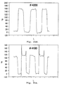
- the transmission of the EPS-PMB #4300 (Fig. 12), the film-incident reflectance (Fig. 13), the substrate-incident reflectance (Fig. 14), the PSI tool measured phase shifts at 325 nm, 488 nm, and 633 nm (Fig. 15), and the second order fit to the PSI data (Fig. 16) are all similar to the values for the EPS-PMB #3700. If the film thickness of #4300 is increased slightly so that its phase shift at 365 nm is equal to that of #3700, the transmission of #4300 at 365 nm will become about 0.055, which is essentially the same as that of #3700.
- three sputtering targets are used to adjust the relative thickness and depthwise proportions of the components in the EPS-PMB, permitting flexible design of the film-incident and substrate-incident reflectances of the EPS-PMB.
- the example illustrates the adjustment of the extinction coefficient of the more strongly absorbing component.
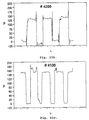
- Photoblanks were produced with process parameters described in Table I under EPS-PMB samples #4100 and #4200. In both cases, one of the three sputtering targets was operated at a substantially higher power than the other two sputtering targets.
- the essential difference between the process parameters for the two EPS-PMBs is that target #2 is the high power target for sample #4100 and target #1 is the high power target for sample #4200.
- target #2 is the high power target for sample #4100
- target #1 is the high power target for sample #4200.
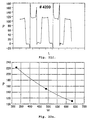
- the more strongly absorbing region of the film is in the center of the film for sample #4100, while for sample #4200, the more strongly absorbing region is adjacent to the substrate-film interface. This difference between absorbing region locations is shown in the compositional depth profiles of the two materials (Fig. 17).
- the depth profiles in Fig. 17 illustrate that the more strongly absorbing region of #4200 has less oxygen than the more strongly absorbing region of #4100.
- the more absorbing region of #4200 will exhibit a higher extinction coefficient than the more absorbing region of #4100.
- We define the extent of the more strongly absorbing region of the film by identifying the locations in the film at which the oxygen concentration undergoes half its total change.
- the oxygen drops from its 0.55 surface concentration to a minimum of 0.35, so the total change in oxygen concentration is 0.20 and half the total change in oxygen concentration is 0.10.
- the more strongly absorbing region of #4100 is then defined as the region in which the oxygen concentration of the film drops below 0.45 (i.e., 0.55-0.10 is 0.45).
- This region extends through roughly 75% of #4100's total film thickness.
- the relative thickness of the more strongly absorbing region of #4200 can be similarly defined, but for #4200 (Fig. 17b) the oxygen concentration drops from about 0.53 in the vicinity of the surface to about 0.27 at its lowest point, and the more strongly absorbing region is defined as the region in which the oxygen concentration drops below 0.40.
- the more strongly absorbing region is seen to occupy about 55% of the total film thickness, smaller than the relative thickness of the more strongly absorbing region of #4100.
- the higher extinction coefficient of #4200's more strongly absorbing region results in a slightly lower transmission than that of #4100, even though the more strongly absorbing region of #4200 occupies a relatively thinner region of the total film thickness.
- This concentration of a more strongly absorbing region with a higher extinction coefficient also imparts a flatter spectral transmission response to sample #4200 than to #4100, as shown in Fig. 18. Lower transmission is important in inspection and alignment of the photomask produced from the photoblank.
- a further difference between #4100 and #4200 is the sheet resistance, as measured by the well known electrometer method.
- #4200's relatively thinner, less oxidic absorbing region imparts to it a lower sheet resistance than does the relatively thicker, more oxidic absorbing region of #4100, as indicated in Table II.
- This is advantageous in electron beam patterning of the photoblank because sheet resistance of the material should be low enough that a charge dissipation layer is not required to pattern the film.
- the desired sheet resistance depends upon the pattern fidelity required, but sheet resistance below about 10 9 ⁇ / ⁇ has been found to be advantageous.
- Sample #4100 has film-incident reflectance of 0.103 and substrate-incident reflectance of 0.149 at the 365 nm use wavelength, while #4200 has film-incident reflectance of 0.152 and substrate-incident reflectance of 0.104 at the 365 nm use wavelength.
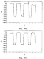
- phase shift measurements for #4100 and #4200 are shown in Fig. 21, and the second order fits to the Fig. 21 data are shown in Fig. 22.
- These data and the data in Table II indicate the phase shifts at the 365 nm use wavelength to be 203° for #4100 and 204° for #4200.
- the depth profile engineering in this example thus allows adjustment of the transmission, sheet resistance, and reflectances of the material, even though the phase shift is essentially unaffected at the 365 nm use wavelength.
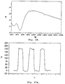
- FIG. 24 A transmission (Fig. 24) and film and substrate incident reflectances (Fig. 25 and Fig. 26) which when combined with the large DUV phase shift of this film (as determined from the PSI scans of Fig. 27 and the second-order fit of Fig. 28) permit one to produce a DUV EPS-PMB having 2.3% transmission at the lithographic wavelength from this material. This is accomplished by producing a film of 907 nm thickness to provide the 2.3% DUV EPS-PMB, using the component materials and relative depth profiles of Fig. 23.
- EPS-PMBs for use at wavelengths other than I-line (365 nm).
- An attenuated blank (#5000) for use at G-line (436 nm) was produced using the process settings presented in Table I for #5000, and has the composition profile shown in Figure 29. It has a transmission (Fig. 30) and film and substrate incident reflectances (as determined from the PSI scan of Fig. 31 and the second-order fit of Fig. 32) which when combined with the G-line phase shift of this film (Fig. 33 and Fig. 34) demonstrates that this is a 6.3% G-line EPS-PMB having 6.3% transmission at the lithographic wavelength.
- Example 1 Example 2, Example 3, Example 4 and Example 5 demonstrate the inherent advantages of the inhomogeneous nature of these films and the versatility of the higher absorbing and less absorbing components of the inhomogeneous attenuating films.
- 150 150 150 150 150 150 150 150 DC Elec. Power: Target #1 KW 0 0 0.82 1.67 0 1.67 DC Elec. Power: Target #2 KW 1.66 1.68 1.68 0.85 2.23 0.86 DC Elec.
Landscapes
- Physics & Mathematics (AREA)
- General Physics & Mathematics (AREA)
- Preparing Plates And Mask In Photomechanical Process (AREA)
- Lasers (AREA)
- Exposure And Positioning Against Photoresist Photosensitive Materials (AREA)
- Investigating Or Analysing Materials By Optical Means (AREA)
Applications Claiming Priority (3)
| Application Number | Priority Date | Filing Date | Title |
|---|---|---|---|
| US195670 | 1994-02-14 | ||
| US08/195,670 US5415953A (en) | 1994-02-14 | 1994-02-14 | Photomask blanks comprising transmissive embedded phase shifter |
| PCT/US1995/001393 WO1995022083A2 (en) | 1994-02-14 | 1995-02-10 | Photomask blanks |
Publications (2)
| Publication Number | Publication Date |
|---|---|
| EP0745235A1 EP0745235A1 (en) | 1996-12-04 |
| EP0745235B1 true EP0745235B1 (en) | 1999-05-06 |
Family
ID=22722290
Family Applications (1)
| Application Number | Title | Priority Date | Filing Date |
|---|---|---|---|
| EP95908787A Expired - Lifetime EP0745235B1 (en) | 1994-02-14 | 1995-02-10 | Photomask blanks |
Country Status (8)
| Country | Link |
|---|---|
| US (1) | US5415953A (enExample) |
| EP (1) | EP0745235B1 (enExample) |
| JP (1) | JP3595860B2 (enExample) |
| KR (1) | KR100362126B1 (enExample) |
| CN (1) | CN1122876C (enExample) |
| DE (1) | DE69509502T2 (enExample) |
| TW (1) | TW316856B (enExample) |
| WO (1) | WO1995022083A2 (enExample) |
Families Citing this family (41)
| Publication number | Priority date | Publication date | Assignee | Title |
|---|---|---|---|---|
| JP3440346B2 (ja) * | 1994-12-22 | 2003-08-25 | 大日本印刷株式会社 | ブラックマトリックス用クロムブランクスおよび液晶デイスプレイ用カラーフイルター |
| DE69523165T2 (de) * | 1995-07-19 | 2002-05-29 | Hoya Corp., Tokio/Tokyo | Phasenschiebermasken-rohling und verfahren zu seiner herstellung |
| KR0147493B1 (ko) * | 1995-10-25 | 1998-08-01 | 김주용 | 하프톤 위상반전마스크 제조방법 |
| US5618643A (en) * | 1995-12-15 | 1997-04-08 | Intel Corporation | Embedded phase shifting mask with improved relative attenuated film transmission |
| US5942356A (en) | 1996-03-30 | 1999-08-24 | Hoya Corporation | Phase shift mask and phase shift mask blank |
| US5897977A (en) * | 1996-05-20 | 1999-04-27 | E. I. Du Pont De Nemours And Company | Attenuating embedded phase shift photomask blanks |
| US5897976A (en) * | 1996-05-20 | 1999-04-27 | E. I. Du Pont De Nemours And Company | Attenuating embedded phase shift photomask blanks |
| TW354392B (en) * | 1996-07-03 | 1999-03-11 | Du Pont | Photomask blanks |
| US5714285A (en) * | 1996-07-17 | 1998-02-03 | Taiwan Semiconductor Manufacturing Company, Ltd | Using (LaNiO3)X (TiO2)1-x oxide absorption composite for attenuating phase shifting blanks and masks |
| US5981109A (en) * | 1996-07-17 | 1999-11-09 | Taiwan Semiconductor Manufacturing Company, Ltd. | Using (LaNiO3) X (TiO2) 1-X and (LaNiO3) X (Ta2 O5) 1-X oxide absorption composites for attenuating phase shifting blanks and masks |
| US6174631B1 (en) | 1997-02-10 | 2001-01-16 | E. I. Du Pont De Nemours And Company | Attenuating phase shift photomasks |
| US6319634B1 (en) | 1999-03-12 | 2001-11-20 | Corning Incorporated | Projection lithography photomasks and methods of making |
| US6682859B2 (en) * | 1999-02-12 | 2004-01-27 | Corning Incorporated | Vacuum ultraviolet trasmitting silicon oxyfluoride lithography glass |
| US6782716B2 (en) * | 1999-02-12 | 2004-08-31 | Corning Incorporated | Vacuum ultraviolet transmitting silicon oxyfluoride lithography glass |
| US6242136B1 (en) | 1999-02-12 | 2001-06-05 | Corning Incorporated | Vacuum ultraviolet transmitting silicon oxyfluoride lithography glass |
| US6783898B2 (en) | 1999-02-12 | 2004-08-31 | Corning Incorporated | Projection lithography photomask blanks, preforms and method of making |
| US6265115B1 (en) | 1999-03-15 | 2001-07-24 | Corning Incorporated | Projection lithography photomask blanks, preforms and methods of making |
| JP2001033938A (ja) * | 1999-07-22 | 2001-02-09 | Oki Electric Ind Co Ltd | ハーフトーン位相シフトマスクの特性補正方法 |
| US6291113B1 (en) | 1999-10-21 | 2001-09-18 | Advanced Micro Devices, Inc. | Sidelobe suppressing phase shift mask and method |
| US6410192B1 (en) | 1999-11-15 | 2002-06-25 | Corning Incorporated | Photolithography method, photolithography mask blanks, and method of making |
| TW480367B (en) * | 2000-02-16 | 2002-03-21 | Shinetsu Chemical Co | Photomask blank, photomask and method of manufacture |
| US6379014B1 (en) * | 2000-04-27 | 2002-04-30 | N & K Technology, Inc. | Graded anti-reflective coatings for photolithography |
| JP3932805B2 (ja) * | 2000-12-25 | 2007-06-20 | 株式会社日立製作所 | フォトマスク及びそれを用いた電子デバイスの製造方法 |
| JP2002244274A (ja) * | 2001-02-13 | 2002-08-30 | Shin Etsu Chem Co Ltd | フォトマスクブランク、フォトマスク及びこれらの製造方法 |
| US6653027B2 (en) | 2001-02-26 | 2003-11-25 | International Business Machines Corporation | Attenuated embedded phase shift photomask blanks |
| JP2003322954A (ja) * | 2002-03-01 | 2003-11-14 | Hoya Corp | ハーフトーン型位相シフトマスクブランク及びハーフトーン型位相シフトマスク |
| US7166392B2 (en) | 2002-03-01 | 2007-01-23 | Hoya Corporation | Halftone type phase shift mask blank and halftone type phase shift mask |
| JP2003322947A (ja) * | 2002-04-26 | 2003-11-14 | Hoya Corp | ハーフトーン型位相シフトマスクブランク及びハーフトーン型位相シフトマスク |
| US6855463B2 (en) * | 2002-08-27 | 2005-02-15 | Photronics, Inc. | Photomask having an intermediate inspection film layer |
| JP2004145065A (ja) * | 2002-10-25 | 2004-05-20 | Toppan Printing Co Ltd | ハーフトーン型位相シフトマスク用ブランク及びその位相シフトマスク及びそのマスクを用いた半導体装置の製造方法 |
| JPWO2004051369A1 (ja) * | 2002-12-03 | 2006-04-06 | Hoya株式会社 | フォトマスクブランク、及びフォトマスク |
| US6859311B2 (en) * | 2003-03-24 | 2005-02-22 | Memphis Eye & Cataract Associates Ambulatory Surgery Center | Digital micromirror device having a window transparent to ultraviolet (UV) light |
| TWI375114B (en) * | 2004-10-22 | 2012-10-21 | Shinetsu Chemical Co | Photomask-blank, photomask and fabrication method thereof |
| DE102009046878A1 (de) * | 2009-07-31 | 2011-02-03 | Advanced Mask Technology Center Gmbh & Co. Kg | Verringerung der lonenwanderung von Absorbermaterialien von Lithographiemasken durch Chrompassivierung |
| TWI588593B (zh) * | 2010-04-09 | 2017-06-21 | Hoya Corp | Phase shift mask substrate and method of making same, and phase shift mask |
| JP6198238B2 (ja) * | 2013-04-17 | 2017-09-20 | アルバック成膜株式会社 | 位相シフトマスクの製造方法 |
| KR102145934B1 (ko) * | 2014-05-20 | 2020-08-19 | 동우 화인켐 주식회사 | 광경화 패턴의 형성 방법 |
| JP6341166B2 (ja) * | 2015-09-03 | 2018-06-13 | 信越化学工業株式会社 | フォトマスクブランク |
| JP6812236B2 (ja) * | 2016-12-27 | 2021-01-13 | Hoya株式会社 | 位相シフトマスクブランク及びこれを用いた位相シフトマスクの製造方法、並びに表示装置の製造方法 |
| JP6999460B2 (ja) * | 2018-03-23 | 2022-01-18 | Hoya株式会社 | 位相シフトマスクブランク、位相シフトマスク中間体及びこれらを用いた位相シフトマスクの製造方法、並びに表示装置の製造方法 |
| JP7255512B2 (ja) * | 2019-03-29 | 2023-04-11 | 信越化学工業株式会社 | 位相シフトマスクブランク及び位相シフトマスク |
Family Cites Families (10)
| Publication number | Priority date | Publication date | Assignee | Title |
|---|---|---|---|---|
| DD126361A1 (enExample) * | 1976-04-30 | 1977-07-13 | ||
| JPS57121226A (en) * | 1981-01-21 | 1982-07-28 | Hitachi Ltd | Photo mask |
| JPS61272746A (ja) * | 1985-05-28 | 1986-12-03 | Asahi Glass Co Ltd | フオトマスクブランクおよびフオトマスク |
| US4890309A (en) * | 1987-02-25 | 1989-12-26 | Massachusetts Institute Of Technology | Lithography mask with a π-phase shifting attenuator |
| JP2765016B2 (ja) * | 1989-03-15 | 1998-06-11 | 凸版印刷株式会社 | フオトマスクブランクおよびフオトマスク |
| JPH04125643A (ja) * | 1990-09-18 | 1992-04-27 | Toppan Printing Co Ltd | フォトマスクおよびフォトマスクブランク |
| US5230971A (en) * | 1991-08-08 | 1993-07-27 | E. I. Du Pont De Nemours And Company | Photomask blank and process for making a photomask blank using gradual compositional transition between strata |
| US5187726A (en) * | 1991-09-30 | 1993-02-16 | Wisconsin Alumni Research Foundation | High resolution X-ray lithography using phase shift masks |
| JP3160332B2 (ja) * | 1991-11-01 | 2001-04-25 | 大日本印刷株式会社 | ハーフトーン位相シフトフォトマスク |
| TW505829B (en) * | 1992-11-16 | 2002-10-11 | Dupont Photomasks Inc | A transmissive embedded phase shifter-photomask blank |
-
1994
- 1994-02-14 US US08/195,670 patent/US5415953A/en not_active Expired - Lifetime
-
1995
- 1995-01-06 TW TW084100067A patent/TW316856B/zh active
- 1995-02-10 CN CN95191612A patent/CN1122876C/zh not_active Expired - Fee Related
- 1995-02-10 EP EP95908787A patent/EP0745235B1/en not_active Expired - Lifetime
- 1995-02-10 WO PCT/US1995/001393 patent/WO1995022083A2/en not_active Ceased
- 1995-02-10 KR KR1019960704398A patent/KR100362126B1/ko not_active Expired - Fee Related
- 1995-02-10 DE DE69509502T patent/DE69509502T2/de not_active Expired - Fee Related
- 1995-02-10 JP JP52126395A patent/JP3595860B2/ja not_active Expired - Fee Related
Also Published As
| Publication number | Publication date |
|---|---|
| TW316856B (enExample) | 1997-10-01 |
| DE69509502D1 (de) | 1999-06-10 |
| CN1145124A (zh) | 1997-03-12 |
| KR970701379A (ko) | 1997-03-17 |
| WO1995022083A3 (en) | 1995-10-19 |
| KR100362126B1 (ko) | 2003-04-10 |
| DE69509502T2 (de) | 1999-09-02 |
| EP0745235A1 (en) | 1996-12-04 |
| US5415953A (en) | 1995-05-16 |
| WO1995022083A2 (en) | 1995-08-17 |
| JP3595860B2 (ja) | 2004-12-02 |
| JPH09508981A (ja) | 1997-09-09 |
| CN1122876C (zh) | 2003-10-01 |
Similar Documents
| Publication | Publication Date | Title |
|---|---|---|
| EP0745235B1 (en) | Photomask blanks | |
| EP0670054B1 (en) | Photomask blanks | |
| KR102003650B1 (ko) | 위상 시프트 마스크 블랭크 및 이것을 사용한 위상 시프트 마스크의 제조 방법, 및 표시 장치의 제조 방법 | |
| KR100213151B1 (ko) | 감쇠하는 상 이동 마스크의 제조를 위한 박막의 물질 | |
| KR101333929B1 (ko) | 포토마스크 블랭크, 포토마스크와 그 제조 방법, 및 반도체 장치의 제조 방법 | |
| TWI541589B (zh) | A mask blank and its manufacturing method, manufacturing method of a mask, and manufacturing method of a semiconductor device | |
| CN108241251B (zh) | 相移掩模坯料、相移掩模制造方法及显示装置制造方法 | |
| US6395433B1 (en) | Photomask for projection lithography at or below about 160 nm and a method thereof | |
| JP2009122566A (ja) | 低反射型フォトマスクブランクスおよびフォトマスク | |
| KR20190078506A (ko) | 포토마스크 블랭크 및 포토마스크의 제조 방법, 및 표시 장치의 제조 방법 | |
| KR20010089414A (ko) | 하프톤 위상 시프트 포토 마스크 및 이를 제작하기 위한하프톤 위상 시프트 포토 마스크용 블랭크 | |
| JP3478067B2 (ja) | ハーフトーン型位相シフトマスク及びハーフトーン型位相シフトマスク用ブランク | |
| KR20160046285A (ko) | 플랫 패널 디스플레이용 위상 반전 블랭크 마스크 및 포토마스크 | |
| JP3351892B2 (ja) | ハーフトーン位相シフトフォトマスク及びハーフトーン位相シフトフォトマスク用ブランクス | |
| JP3289606B2 (ja) | ハーフトーン型位相シフトマスク用ブランク及びハーフトーン型位相シフトマスク | |
| JPH1184624A (ja) | ハーフトーン型位相シフトマスク用ブランク及びハーフトーン型位相シフトマスク及びそれらの製造方法 | |
| KR101155415B1 (ko) | 하프톤형 위상반전 블랭크 마스크 및 그 제조방법 | |
| Chiba et al. | Antireflective MoSi photomasks | |
| JP2003005349A (ja) | ハーフトーン型位相シフトマスク用ブランクおよびハーフトーン型位相シフトマスク | |
| JP2003084418A (ja) | ハーフトーン型位相シフトマスクおよびブランク | |
| JPH10161294A (ja) | ハーフトーン型位相シフトマスク用ブランク及びハーフトーン型位相シフトマスク及びそれらの製造方法 | |
| Kanayama et al. | ZrSiON as a material for high-transmittance attenuated PSM |
Legal Events
| Date | Code | Title | Description |
|---|---|---|---|
| PUAI | Public reference made under article 153(3) epc to a published international application that has entered the european phase |
Free format text: ORIGINAL CODE: 0009012 |
|
| 17P | Request for examination filed |
Effective date: 19960711 |
|
| AK | Designated contracting states |
Kind code of ref document: A1 Designated state(s): DE FR GB IT NL |
|
| 17Q | First examination report despatched |
Effective date: 19961113 |
|
| RAP1 | Party data changed (applicant data changed or rights of an application transferred) |
Owner name: DU PONT PHOTOMASKS, INC. |
|
| GRAG | Despatch of communication of intention to grant |
Free format text: ORIGINAL CODE: EPIDOS AGRA |
|
| GRAG | Despatch of communication of intention to grant |
Free format text: ORIGINAL CODE: EPIDOS AGRA |
|
| GRAH | Despatch of communication of intention to grant a patent |
Free format text: ORIGINAL CODE: EPIDOS IGRA |
|
| GRAH | Despatch of communication of intention to grant a patent |
Free format text: ORIGINAL CODE: EPIDOS IGRA |
|
| GRAA | (expected) grant |
Free format text: ORIGINAL CODE: 0009210 |
|
| ITF | It: translation for a ep patent filed | ||
| AK | Designated contracting states |
Kind code of ref document: B1 Designated state(s): DE FR GB IT NL |
|
| REF | Corresponds to: |
Ref document number: 69509502 Country of ref document: DE Date of ref document: 19990610 |
|
| ET | Fr: translation filed | ||
| PLBE | No opposition filed within time limit |
Free format text: ORIGINAL CODE: 0009261 |
|
| STAA | Information on the status of an ep patent application or granted ep patent |
Free format text: STATUS: NO OPPOSITION FILED WITHIN TIME LIMIT |
|
| 26N | No opposition filed | ||
| REG | Reference to a national code |
Ref country code: GB Ref legal event code: IF02 |
|
| REG | Reference to a national code |
Ref country code: GB Ref legal event code: 732E |
|
| REG | Reference to a national code |
Ref country code: FR Ref legal event code: TP |
|
| NLS | Nl: assignments of ep-patents |
Owner name: SCHOTT LITHOTEC AG |
|
| PGFP | Annual fee paid to national office [announced via postgrant information from national office to epo] |
Ref country code: NL Payment date: 20090217 Year of fee payment: 15 Ref country code: DE Payment date: 20090219 Year of fee payment: 15 |
|
| PGFP | Annual fee paid to national office [announced via postgrant information from national office to epo] |
Ref country code: GB Payment date: 20090219 Year of fee payment: 15 |
|
| PGFP | Annual fee paid to national office [announced via postgrant information from national office to epo] |
Ref country code: IT Payment date: 20090221 Year of fee payment: 15 |
|
| PGFP | Annual fee paid to national office [announced via postgrant information from national office to epo] |
Ref country code: FR Payment date: 20090213 Year of fee payment: 15 |
|
| REG | Reference to a national code |
Ref country code: NL Ref legal event code: V1 Effective date: 20100901 |
|
| GBPC | Gb: european patent ceased through non-payment of renewal fee |
Effective date: 20100210 |
|
| REG | Reference to a national code |
Ref country code: FR Ref legal event code: ST Effective date: 20101029 |
|
| PG25 | Lapsed in a contracting state [announced via postgrant information from national office to epo] |
Ref country code: NL Free format text: LAPSE BECAUSE OF NON-PAYMENT OF DUE FEES Effective date: 20100901 Ref country code: FR Free format text: LAPSE BECAUSE OF NON-PAYMENT OF DUE FEES Effective date: 20100301 |
|
| PG25 | Lapsed in a contracting state [announced via postgrant information from national office to epo] |
Ref country code: DE Free format text: LAPSE BECAUSE OF NON-PAYMENT OF DUE FEES Effective date: 20100901 |
|
| PG25 | Lapsed in a contracting state [announced via postgrant information from national office to epo] |
Ref country code: IT Free format text: LAPSE BECAUSE OF NON-PAYMENT OF DUE FEES Effective date: 20100210 Ref country code: GB Free format text: LAPSE BECAUSE OF NON-PAYMENT OF DUE FEES Effective date: 20100210 |