EP0740460A2 - Bildlesegerät - Google Patents
Bildlesegerät Download PDFInfo
- Publication number
- EP0740460A2 EP0740460A2 EP96106563A EP96106563A EP0740460A2 EP 0740460 A2 EP0740460 A2 EP 0740460A2 EP 96106563 A EP96106563 A EP 96106563A EP 96106563 A EP96106563 A EP 96106563A EP 0740460 A2 EP0740460 A2 EP 0740460A2
- Authority
- EP
- European Patent Office
- Prior art keywords
- color
- linear
- color image
- linear image
- signals
- Prior art date
- Legal status (The legal status is an assumption and is not a legal conclusion. Google has not performed a legal analysis and makes no representation as to the accuracy of the status listed.)
- Withdrawn
Links
Images



Classifications
-
- H—ELECTRICITY
- H04—ELECTRIC COMMUNICATION TECHNIQUE
- H04N—PICTORIAL COMMUNICATION, e.g. TELEVISION
- H04N1/00—Scanning, transmission or reproduction of documents or the like, e.g. facsimile transmission; Details thereof
- H04N1/46—Colour picture communication systems
- H04N1/48—Picture signal generators
- H04N1/486—Picture signal generators with separate detectors, each detector being used for one specific colour component
Definitions
- the present invention relates to an image reading apparatus, and more particularly, to an image reading apparatus which compensates inter-deviations of an RGB balance which is created when a linear image sensor which comprises three linear image sensors for R, G and B successive reads scanning lines on a color original.
- an image reading apparatus such as a color process scanner for manufacturing a plate, which digitally reads an image
- three linear image sensors are disposed parallel to each other in correspondence to optical color components of red, green and blue (hereinafter "R,” “G” and “B") which are to be read.
- Each linear image sensor is formed by arranging a plurality of CCD elements in a line, and a color filter (R-, G- or B-filter) is disposed on each linear image sensor.
- the respective linear image sensors read R-, G- and B-components of the original pixel by pixel. Based on image data or corrected version of the image data regarding each color component which is read in this manner, a recorded image (color-separated image or reproduced color image) is generated.
- Fig. 6 is a graph showing such a difference in the sensitivities.
- an incident wavelength is measured along a horizontal axis and a relative sensitivity (which is an output level which is obtained when light having a uniform distribution all over the visible light band range impinges upon the sensors) is measured along a vertical axis.
- the R-linear image sensor is sensitive to light belonging to a wavelength band range of 600-700 nm, exhibiting the highest output level.
- the G-linear image sensor is sensitive to light belonging to a wavelength band range of 500-600 nm, exhibiting an intermediate output level.
- the B-linear image sensor is sensitive to light belonging to a wavelength band range of 400-500 nm, exhibiting the lowest output level. That is, the sensitivity of the R-linear image sensor is highest, and the G-linear image sensor and the B-linear image sensor have successively decreasing sensitivities in this order.
- a first group of such conventional techniques is related to an apparatus for reading a monochrome image, and unlike the present invention is not related to an apparatus which compensates inter-deviations of and a change in color balances of a light source and each linear image sensor.
- the respective conventional techniques detect only the brightness (luminance) of a light source and control a charge accumulating time of a CCD based on a detected change in the brightness.
- a second group of the conventional techniques uses means (specifically, a photodiode) for detecting a change in the quantity of light, in addition to CCDs, which makes the structure complex.
- the present invention is directed to a color image reader.
- the color image reader comprises a) a plurality of linear image sensors for reading a color image to generate a plurality of color component signals representative of respective color components of the color image, respectively, b) timing generator means for generating a plurality of timing signals for determining respective time periods in which the plurality of linear image sensors are enabled, respectively, c) means for enabling the plurality of linear image sensors to read a reference color image to obtain a plurality of reference color component signals, and d) feedback means for controlling the respective time periods such that respective levels of the reference color component signals are within a predetermined range, respectively.
- the charge accumulating time is optimized within each linear image sensor, whereby the balance of a plurality of color component signals becomes uniform at an output side of each linear image sensor.
- the color image reader further comprises e) means for relatively moving the plurality of linear image sensors and the color image to thereby scan the color image for each scanning line, f) means for generating a start timing signal for defining a start timing of reading each scanning line, wherein the feedback means is operable to control the respective time periods independently of the start timing signal.
- the present invention is also directed to a method of compensating photo-sensitivities of a plurality of linear image sensors included in a color image reader for reading respective color components of a color image.
- the method comprises the steps of a) generating a plurality of timing signals for determining respective time periods in which the plurality of linear image sensors are enabled, respectively, b) transmitting the plurality of timing signals to the plurality of image sensors to read a reference color image to thereby obtain a plurality of reference color component signals, and c) controlling the respective time periods such that respective levels of the reference color component signals are within a predetermined range, respectively.
- an object of the present invention is to provide for an image reading apparatus which compensates inter-deviations of and a change in a color temperature of a light source while compensating a difference in the sensitivities between linear image sensors and a change in the sensitivity difference.
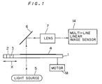
- Fig. 1 is a view showing a simplified structure of an image reading apparatus according to a preferred embodiment of the present invention.
- a motor M is connected to an original table 1 so that the original table 1 is movable in a direction X.
- a black reference board 2 and a white reference board 3 are disposed in the vicinity of one of the edges of the original table 1.
- the black reference board 2 and the white reference board 3 are read before reading an original, to thereby perform various types of correction.
- An original 4 to be read is mounted on the original table 1.
- Light from a light source 5 passes through the original table 1 and the original 4, and is reflected by a mirror 6 to impinge upon a lens 7.
- the lens 7 forms an image of the original 4 on a reading surface of a multi-line linear image sensor 14.
- the multi-line linear image sensor 14 successively reads the image of the original 4 scanning line by scanning line, as the original table 1 moves.
- the longitudinal direction of the multi-line linear image sensor 14 is a main scanning direction
- the direction in which the original table 1 moves is a sub scanning direction.
- Fig. 2 is a block diagram showing an electric structure according to the preferred embodiment shown in Fig. 1.
- the image reading apparatus comprises a CPU bus 9, a CPU 10, a ROM 11, a RAM 12, a timing generator 13, the multi-line linear image sensor 14, an amplifying & sample hold circuit 15, an A/D convertor 16, a signal processing circuit 17, and a line memory 18.
- the CPU 10, the ROM 11, and the RAM 12 are connected to the CPU bus 9.
- the ROM 11 stores an operation program for the CPU 10 and a proper level of each linear image sensor for the purpose of correcting an RGB balance.
- the CPU 10 operates according to the operation program which is stored in the ROM 11 and controls the respective circuits which are connected to the CPU bus 9.
- the RAM 12 serves as a working memory, storing various types of data which are necessary for the CPU 10 to process data.
- the timing generator 13 is also connected to the CPU bus 9.
- the timing generator 13 generates four types of timing signals LST, IG-R, IG-G, and IG-B, in response to an instruction from the CPU 10. These timing signals are supplied to the multi-line linear image sensor 14.
- the multi-line linear image sensor 14 includes three linear image sensors which extend in the main scanning direction, i.e., an R-linear image sensor 14R, a G-linear image sensor 14G and a B-linear image sensor 14B.
- the linear image sensors are each formed by arranging a plurality of CCD elements for R, G and B, respectively, in a line.
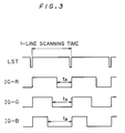
- Fig. 3 is a timing chart showing the timing signals LST, IG-R, IG-G, and IG-B.
- the timing signal LST start timing signal
- the timing signals IG-R, IG-G, and IG-B are pulse signals and are supplied respectively to the R-linear image sensor, the G-linear image sensor and the B-linear image sensor, independently of each other, to define a charge accumulating time of each linear image sensor.
- the timing signals IG-R, IG-G and IG-B are activated at a first time and inactivated at a second time.
- the first time is different for the three timing signals, whilst the second time is common to the three timing signals.
- the R-, the G-, and the B-linear image sensors convert light from the lens 7 into electric charges and accumulate the electric charges, within periods t R , t G and t B which are defined respectively by the timing signals IG-R, IG-G, and IG-B.
- three primary color signals R, G and B are outputted from the multi-line linear image sensor 14, are supplied to the A/D converter 16, and are converted into three digital primary color signals.
- the three digital primary color signals are supplied to the signal processing circuit 17 and the line memory 18.
- An output signal from the image reading apparatus is available from the signal processing circuit 17.
- the line memory 18 includes memories for three lines, and stores the three digital primary color signals separately from each other.
- the three digital primary color signals which are stored in the line memory 18 are referred to by the CPU 10 and are used to correct the RGB balance.
- Fig. 4 is a flow chart showing the operation of the image reading apparatus of Fig. 1
- Fig. 5 is a graph showing output values from the CCD elements of the respective linear image sensors of the multi-line linear image sensor 14.
- the CPU 10 sets the low level periods t R , t G and t B of the timing signals IG-R, IG-G, and IG-B which are generated by the timing generator 13 (See Fig. 3) at default values which are stored in the apparatus in advance (e.g., within the ROM 11) (Step S1).
- the default values may be any values in principle, the default values are preferably values which are selected considering inter-deviations of the RGB balance on the linear image sensor side. Since this allows each linear image sensor to output an output value which is close to the appropriate range from the beginning, it is possible to complete correction of the charge accumulating times which will follow later, within a shorter period of time.
- the CPU 10 moves the original table 1 to a position at which the multi-line linear image sensor 14 can read the white reference board 3 (Step S2). Hence, the multi-line linear image sensor 14 reads the white reference board 3 (Step S3). Image data of the white reference board 3 which is read by the multi-line linear image sensor 14 is converted into three digital primary color signals and is then temporarily stored in the line memory 18 (Step S4). Next, the CPU 10 selects a digital color signal for one line from digital signals for three lines which are stored in the line memory 18, compares output levels associated with the respective pixels included in the selected color signal, and detects a peak value V MAX (See Fig. 5) (Step S5).
- the ROM 11 stores an upper limit value V H and a lower limit value V L which define the appropriate range as that shown in Fig. 5.
- the charge accumulating time of a CCD of each linear image sensor is corrected until the peak value V MAX enters the appropriate range.
- the appropriate range is selected as high as possible but so as not to allow saturation of a CCD output from each linear image sensor. Hence, it is possible to increase accumulated charges and an S/N ratio of an image reading signal. If the appropriate range is selected as a saturation region, blooming, i.e., a phenomena that excessive charges are transferred to adjacent CCDs, is created to thereby deteriorate the S/N ratio.
- Step S6 if the peak value V MAX is not over the upper limit value V H , the CPU 10 judges whether the peak value V MAX is lower than the lower limit value V L (Step S8). If the peak value V MAX is lower than the lower limit value V L (i.e., in the case of P2 in Fig. 5), the CPU 10 instructs the timing generator 13 to extend the low level period t X of the timing signal IG-X by a predetermined period of time (Step S9). This extends the charge accumulating time of the CCDs of the associated linear image sensor, and hence increases the output value from this linear image sensor. As a result, the peak value V MAX is increased. Next, the CPU 10 returns to the operation at Step S3 to adjust the low level period t X of the timing signal IG-X in accordance with the data which is read from the white reference board 3.
- Step S9 The operations from Step S3 to Step S9 are repeated, whereby the peak value V MAX gradually becomes close to the appropriate range.
- V MAX ⁇ V H and V MAX ⁇ V L so that the CPU 10 sets the low level period t X of the timing signal IG-X at this stage within the timing generator 13, as a final result of correction (Step S10).
- the CPU 10 judges whether such correction as above of the charge accumulating time is complete for every linear image sensor which is included in the multi-line linear image sensor 14 (Step S11). If there is a linear image sensor on which such correction is not complete yet, the CPU 10 returns to the operation at Step S3 to repeat the series of correction operations described above. The CPU 10 finishes operating upon completion of correction on all linear image sensors.
Landscapes
- Engineering & Computer Science (AREA)
- Multimedia (AREA)
- Signal Processing (AREA)
- Facsimile Scanning Arrangements (AREA)
Applications Claiming Priority (2)
| Application Number | Priority Date | Filing Date | Title |
|---|---|---|---|
| JP106622/95 | 1995-04-28 | ||
| JP7106622A JPH08307601A (ja) | 1995-04-28 | 1995-04-28 | 画像読取装置 |
Publications (2)
| Publication Number | Publication Date |
|---|---|
| EP0740460A2 true EP0740460A2 (de) | 1996-10-30 |
| EP0740460A3 EP0740460A3 (de) | 1997-05-07 |
Family
ID=14438217
Family Applications (1)
| Application Number | Title | Priority Date | Filing Date |
|---|---|---|---|
| EP96106563A Withdrawn EP0740460A3 (de) | 1995-04-28 | 1996-04-25 | Bildlesegerät |
Country Status (3)
| Country | Link |
|---|---|
| US (1) | US5880859A (de) |
| EP (1) | EP0740460A3 (de) |
| JP (1) | JPH08307601A (de) |
Cited By (5)
| Publication number | Priority date | Publication date | Assignee | Title |
|---|---|---|---|---|
| EP0788275A3 (de) * | 1996-01-31 | 1998-09-16 | Hewlett-Packard Company | Verfahren und Vorrichtung zur dynamischen Weisspunktveränderung |
| EP0831638A3 (de) * | 1996-09-18 | 2000-02-23 | Fuji Photo Film Co., Ltd. | Verfahren und Gerät zur Speicherung von Bilddaten |
| US6628848B1 (en) | 1997-12-17 | 2003-09-30 | Fuji Photo Film Co., Ltd. | Image reading apparatus |
| EP1379069A1 (de) * | 2002-07-02 | 2004-01-07 | Agfa-Gevaert AG | Vorrichtung und Verfahren zum Erfassen von Bildinformationen einer Bildvorlage |
| EP1729504A3 (de) * | 2005-06-02 | 2010-05-26 | Xerox Corporation | System zur Steuerung des Bilddatenablesens aus einer Abbildungsvorrichtung |
Families Citing this family (10)
| Publication number | Priority date | Publication date | Assignee | Title |
|---|---|---|---|---|
| JP3482795B2 (ja) * | 1996-12-17 | 2004-01-06 | ミノルタ株式会社 | 画像読み取り装置 |
| JPH11146158A (ja) * | 1997-11-11 | 1999-05-28 | Fuji Photo Optical Co Ltd | 画像読取装置 |
| US6943837B1 (en) * | 1999-12-31 | 2005-09-13 | Intel Corporation | Method and apparatus for colormetric channel balancing for solid state image sensor using time division multiplexed sampling waveforms |
| CN1599404A (zh) * | 2000-02-03 | 2005-03-23 | 松下电器产业株式会社 | 图像输入装置 |
| US7317559B2 (en) * | 2002-04-05 | 2008-01-08 | Canon Kabushiki Kaisha | Imaging device and imaging method for use in such device |
| JP4166587B2 (ja) * | 2003-01-24 | 2008-10-15 | 株式会社サキコーポレーション | 外観検査装置および体積検査方法 |
| US8004726B2 (en) * | 2007-02-02 | 2011-08-23 | Kabushiki Kaisha Toshiba | Image reading apparatus and image density correction method |
| JP5797068B2 (ja) * | 2011-09-05 | 2015-10-21 | キヤノン株式会社 | 画像形成装置及び濃度および色の補正を行う方法 |
| JP6142815B2 (ja) * | 2014-02-13 | 2017-06-07 | ブラザー工業株式会社 | 画像読取装置 |
| ES2879613T3 (es) * | 2014-10-22 | 2021-11-22 | Silvia Colagrande | Escáner lineal de imágenes y método de escaneo de imágenes |
Family Cites Families (12)
| Publication number | Priority date | Publication date | Assignee | Title |
|---|---|---|---|---|
| JPS5398721A (en) * | 1977-02-09 | 1978-08-29 | Hitachi Ltd | Facisimile transmitter |
| JPS60236570A (ja) * | 1984-05-10 | 1985-11-25 | Dainippon Screen Mfg Co Ltd | 画像の読取り補正方法 |
| JPS60236569A (ja) * | 1984-05-10 | 1985-11-25 | Dainippon Screen Mfg Co Ltd | 画像読取り補正方法 |
| US4661843A (en) * | 1984-07-16 | 1987-04-28 | Kabushiki Kaisha Toshiba | Color image copying apparatus |
| US4731661A (en) * | 1984-11-16 | 1988-03-15 | Sharp Kabushiki Kaisha | Color document reader with white balance adjuster for determining light emission periods for a plurality of different-colored light sources and corresponding integration times for a light sensor by reading a white reference area |
| FR2577669B1 (fr) * | 1985-02-21 | 1992-05-15 | Fuji Photo Film Co Ltd | Procede et appareil de lecture d'image |
| US4814864A (en) * | 1987-05-29 | 1989-03-21 | Eastman Kodak Co. | Video camera with automatic prescaling for color balance |
| JPH0620221B2 (ja) * | 1987-07-15 | 1994-03-16 | 大日本スクリ−ン製造株式会社 | 読取りタイミングを相対的にずらせた画像読取り装置 |
| JPH02268062A (ja) * | 1989-04-10 | 1990-11-01 | Canon Inc | 光電変換装置 |
| JP3222499B2 (ja) * | 1991-09-12 | 2001-10-29 | 株式会社リコー | デジタルスキャナ |
| JPH05328040A (ja) * | 1992-05-21 | 1993-12-10 | Fujitsu General Ltd | イメージスキャナ装置 |
| CA2108811C (en) * | 1992-10-23 | 2000-05-16 | Toshio Hayashi | Image reading apparatus, copying apparatus, image processing apparatus, and image processing method |
-
1995
- 1995-04-28 JP JP7106622A patent/JPH08307601A/ja active Pending
-
1996
- 1996-04-25 US US08/636,505 patent/US5880859A/en not_active Expired - Fee Related
- 1996-04-25 EP EP96106563A patent/EP0740460A3/de not_active Withdrawn
Cited By (6)
| Publication number | Priority date | Publication date | Assignee | Title |
|---|---|---|---|---|
| EP0788275A3 (de) * | 1996-01-31 | 1998-09-16 | Hewlett-Packard Company | Verfahren und Vorrichtung zur dynamischen Weisspunktveränderung |
| EP0831638A3 (de) * | 1996-09-18 | 2000-02-23 | Fuji Photo Film Co., Ltd. | Verfahren und Gerät zur Speicherung von Bilddaten |
| US6628848B1 (en) | 1997-12-17 | 2003-09-30 | Fuji Photo Film Co., Ltd. | Image reading apparatus |
| EP1379069A1 (de) * | 2002-07-02 | 2004-01-07 | Agfa-Gevaert AG | Vorrichtung und Verfahren zum Erfassen von Bildinformationen einer Bildvorlage |
| EP1729504A3 (de) * | 2005-06-02 | 2010-05-26 | Xerox Corporation | System zur Steuerung des Bilddatenablesens aus einer Abbildungsvorrichtung |
| US7812872B2 (en) | 2005-06-02 | 2010-10-12 | Xerox Corporation | System for controlling image data readout from an imaging device |
Also Published As
| Publication number | Publication date |
|---|---|
| JPH08307601A (ja) | 1996-11-22 |
| US5880859A (en) | 1999-03-09 |
| EP0740460A3 (de) | 1997-05-07 |
Similar Documents
| Publication | Publication Date | Title |
|---|---|---|
| EP0757473B1 (de) | Bildverarbeitungsgerät und -verfahren | |
| US5880859A (en) | Image reading apparatus | |
| US6069973A (en) | Method and apparatus for color correction in a multi-chip imaging array | |
| US7750950B2 (en) | Image pickup apparatus and image processing method | |
| EP1455523B1 (de) | Verfahren und System zum Kalibrieren einer Abtastvorrichtung | |
| US6271940B1 (en) | Color negative scanning and transforming into colors of original scene | |
| EP0267793B1 (de) | Farbbildlesegerät | |
| EP0862336B1 (de) | Automatische Weissabgleichdetektion und Korrektur eines in einer digitalen Kamera aufgenommenen Bildes | |
| EP0268439B2 (de) | Bildlesevorrichtung | |
| US5253083A (en) | Image reading apparatus having improved shading correction | |
| US7643072B2 (en) | Signal processing method for image capturing apparatus, and image capturing apparatus including calculating image transfer efficiency | |
| US6958834B1 (en) | Image reading apparatus | |
| CN1988594A (zh) | 图像处理电路和图像处理方法 | |
| EP0840499B1 (de) | Farbbildabtastgerät | |
| US6806870B1 (en) | Image display control apparatus including adjustment based on brightness | |
| US20040184116A1 (en) | Image inputting apparatus | |
| US7889404B2 (en) | Image reading device, image forming apparatus, and reading-unit install method | |
| JPH117523A (ja) | 画像読取装置 | |
| US7619783B2 (en) | Scanner analog-front-end calibration using percent of freedom | |
| JP2720967B2 (ja) | カラーネガフィルム読取装置 | |
| JP2617925B2 (ja) | 画像読取装置 | |
| JP2971522B2 (ja) | 画像読取装置 | |
| KR100242025B1 (ko) | 쉐이딩 보정을 이용한 칼라 화상 스캐닝 장치 및 방법 | |
| JPH07298046A (ja) | 画像読取り装置 | |
| JPH0787281A (ja) | 原稿読取装置 |
Legal Events
| Date | Code | Title | Description |
|---|---|---|---|
| PUAI | Public reference made under article 153(3) epc to a published international application that has entered the european phase |
Free format text: ORIGINAL CODE: 0009012 |
|
| AK | Designated contracting states |
Kind code of ref document: A2 Designated state(s): DE FR GB |
|
| PUAL | Search report despatched |
Free format text: ORIGINAL CODE: 0009013 |
|
| AK | Designated contracting states |
Kind code of ref document: A3 Designated state(s): DE FR GB |
|
| 17P | Request for examination filed |
Effective date: 19970603 |
|
| 17Q | First examination report despatched |
Effective date: 19990212 |
|
| STAA | Information on the status of an ep patent application or granted ep patent |
Free format text: STATUS: THE APPLICATION IS DEEMED TO BE WITHDRAWN |
|
| 18D | Application deemed to be withdrawn |
Effective date: 19990623 |