EP0738031A2 - Vorrichtung mit kurzwellenlängiger Lichtquelle - Google Patents
Vorrichtung mit kurzwellenlängiger Lichtquelle Download PDFInfo
- Publication number
- EP0738031A2 EP0738031A2 EP96110043A EP96110043A EP0738031A2 EP 0738031 A2 EP0738031 A2 EP 0738031A2 EP 96110043 A EP96110043 A EP 96110043A EP 96110043 A EP96110043 A EP 96110043A EP 0738031 A2 EP0738031 A2 EP 0738031A2
- Authority
- EP
- European Patent Office
- Prior art keywords
- laser
- light source
- optical element
- source apparatus
- short wavelength
- Prior art date
- Legal status (The legal status is an assumption and is not a legal conclusion. Google has not performed a legal analysis and makes no representation as to the accuracy of the status listed.)
- Granted
Links
Images


Classifications
-
- H—ELECTRICITY
- H01—ELECTRIC ELEMENTS
- H01S—DEVICES USING THE PROCESS OF LIGHT AMPLIFICATION BY STIMULATED EMISSION OF RADIATION [LASER] TO AMPLIFY OR GENERATE LIGHT; DEVICES USING STIMULATED EMISSION OF ELECTROMAGNETIC RADIATION IN WAVE RANGES OTHER THAN OPTICAL
- H01S3/00—Lasers, i.e. devices using stimulated emission of electromagnetic radiation in the infrared, visible or ultraviolet wave range
- H01S3/09—Processes or apparatus for excitation, e.g. pumping
- H01S3/091—Processes or apparatus for excitation, e.g. pumping using optical pumping
- H01S3/094—Processes or apparatus for excitation, e.g. pumping using optical pumping by coherent light
- H01S3/0941—Processes or apparatus for excitation, e.g. pumping using optical pumping by coherent light of a laser diode
- H01S3/09415—Processes or apparatus for excitation, e.g. pumping using optical pumping by coherent light of a laser diode the pumping beam being parallel to the lasing mode of the pumped medium, e.g. end-pumping
-
- H—ELECTRICITY
- H01—ELECTRIC ELEMENTS
- H01S—DEVICES USING THE PROCESS OF LIGHT AMPLIFICATION BY STIMULATED EMISSION OF RADIATION [LASER] TO AMPLIFY OR GENERATE LIGHT; DEVICES USING STIMULATED EMISSION OF ELECTROMAGNETIC RADIATION IN WAVE RANGES OTHER THAN OPTICAL
- H01S3/00—Lasers, i.e. devices using stimulated emission of electromagnetic radiation in the infrared, visible or ultraviolet wave range
- H01S3/10—Controlling the intensity, frequency, phase, polarisation or direction of the emitted radiation, e.g. switching, gating, modulating or demodulating
- H01S3/106—Controlling the intensity, frequency, phase, polarisation or direction of the emitted radiation, e.g. switching, gating, modulating or demodulating by controlling devices placed within the cavity
- H01S3/108—Controlling the intensity, frequency, phase, polarisation or direction of the emitted radiation, e.g. switching, gating, modulating or demodulating by controlling devices placed within the cavity using non-linear optical devices, e.g. exhibiting Brillouin or Raman scattering
- H01S3/109—Frequency multiplication, e.g. harmonic generation
-
- G—PHYSICS
- G02—OPTICS
- G02F—OPTICAL DEVICES OR ARRANGEMENTS FOR THE CONTROL OF LIGHT BY MODIFICATION OF THE OPTICAL PROPERTIES OF THE MEDIA OF THE ELEMENTS INVOLVED THEREIN; NON-LINEAR OPTICS; FREQUENCY-CHANGING OF LIGHT; OPTICAL LOGIC ELEMENTS; OPTICAL ANALOGUE/DIGITAL CONVERTERS
- G02F1/00—Devices or arrangements for the control of the intensity, colour, phase, polarisation or direction of light arriving from an independent light source, e.g. switching, gating or modulating; Non-linear optics
- G02F1/35—Non-linear optics
- G02F1/353—Frequency conversion, i.e. wherein a light beam is generated with frequency components different from those of the incident light beams
- G02F1/3544—Particular phase matching techniques
- G02F1/3548—Quasi phase matching [QPM], e.g. using a periodic domain inverted structure
-
- G—PHYSICS
- G02—OPTICS
- G02F—OPTICAL DEVICES OR ARRANGEMENTS FOR THE CONTROL OF LIGHT BY MODIFICATION OF THE OPTICAL PROPERTIES OF THE MEDIA OF THE ELEMENTS INVOLVED THEREIN; NON-LINEAR OPTICS; FREQUENCY-CHANGING OF LIGHT; OPTICAL LOGIC ELEMENTS; OPTICAL ANALOGUE/DIGITAL CONVERTERS
- G02F1/00—Devices or arrangements for the control of the intensity, colour, phase, polarisation or direction of light arriving from an independent light source, e.g. switching, gating or modulating; Non-linear optics
- G02F1/35—Non-linear optics
- G02F1/37—Non-linear optics for second-harmonic generation
- G02F1/377—Non-linear optics for second-harmonic generation in an optical waveguide structure
-
- H—ELECTRICITY
- H01—ELECTRIC ELEMENTS
- H01S—DEVICES USING THE PROCESS OF LIGHT AMPLIFICATION BY STIMULATED EMISSION OF RADIATION [LASER] TO AMPLIFY OR GENERATE LIGHT; DEVICES USING STIMULATED EMISSION OF ELECTROMAGNETIC RADIATION IN WAVE RANGES OTHER THAN OPTICAL
- H01S3/00—Lasers, i.e. devices using stimulated emission of electromagnetic radiation in the infrared, visible or ultraviolet wave range
- H01S3/005—Optical devices external to the laser cavity, specially adapted for lasers, e.g. for homogenisation of the beam or for manipulating laser pulses, e.g. pulse shaping
-
- H—ELECTRICITY
- H01—ELECTRIC ELEMENTS
- H01S—DEVICES USING THE PROCESS OF LIGHT AMPLIFICATION BY STIMULATED EMISSION OF RADIATION [LASER] TO AMPLIFY OR GENERATE LIGHT; DEVICES USING STIMULATED EMISSION OF ELECTROMAGNETIC RADIATION IN WAVE RANGES OTHER THAN OPTICAL
- H01S3/00—Lasers, i.e. devices using stimulated emission of electromagnetic radiation in the infrared, visible or ultraviolet wave range
- H01S3/05—Construction or shape of optical resonators; Accommodation of active medium therein; Shape of active medium
- H01S3/08—Construction or shape of optical resonators or components thereof
- H01S3/08018—Mode suppression
- H01S3/08022—Longitudinal modes
- H01S3/08031—Single-mode emission
-
- H—ELECTRICITY
- H01—ELECTRIC ELEMENTS
- H01S—DEVICES USING THE PROCESS OF LIGHT AMPLIFICATION BY STIMULATED EMISSION OF RADIATION [LASER] TO AMPLIFY OR GENERATE LIGHT; DEVICES USING STIMULATED EMISSION OF ELECTROMAGNETIC RADIATION IN WAVE RANGES OTHER THAN OPTICAL
- H01S3/00—Lasers, i.e. devices using stimulated emission of electromagnetic radiation in the infrared, visible or ultraviolet wave range
- H01S3/09—Processes or apparatus for excitation, e.g. pumping
- H01S3/091—Processes or apparatus for excitation, e.g. pumping using optical pumping
- H01S3/094—Processes or apparatus for excitation, e.g. pumping using optical pumping by coherent light
- H01S3/094065—Single-mode pumping
-
- H—ELECTRICITY
- H01—ELECTRIC ELEMENTS
- H01S—DEVICES USING THE PROCESS OF LIGHT AMPLIFICATION BY STIMULATED EMISSION OF RADIATION [LASER] TO AMPLIFY OR GENERATE LIGHT; DEVICES USING STIMULATED EMISSION OF ELECTROMAGNETIC RADIATION IN WAVE RANGES OTHER THAN OPTICAL
- H01S3/00—Lasers, i.e. devices using stimulated emission of electromagnetic radiation in the infrared, visible or ultraviolet wave range
- H01S3/14—Lasers, i.e. devices using stimulated emission of electromagnetic radiation in the infrared, visible or ultraviolet wave range characterised by the material used as the active medium
- H01S3/16—Solid materials
- H01S3/1601—Solid materials characterised by an active (lasing) ion
- H01S3/1603—Solid materials characterised by an active (lasing) ion rare earth
- H01S3/1611—Solid materials characterised by an active (lasing) ion rare earth neodymium
-
- H—ELECTRICITY
- H01—ELECTRIC ELEMENTS
- H01S—DEVICES USING THE PROCESS OF LIGHT AMPLIFICATION BY STIMULATED EMISSION OF RADIATION [LASER] TO AMPLIFY OR GENERATE LIGHT; DEVICES USING STIMULATED EMISSION OF ELECTROMAGNETIC RADIATION IN WAVE RANGES OTHER THAN OPTICAL
- H01S3/00—Lasers, i.e. devices using stimulated emission of electromagnetic radiation in the infrared, visible or ultraviolet wave range
- H01S3/14—Lasers, i.e. devices using stimulated emission of electromagnetic radiation in the infrared, visible or ultraviolet wave range characterised by the material used as the active medium
- H01S3/16—Solid materials
- H01S3/163—Solid materials characterised by a crystal matrix
- H01S3/1671—Solid materials characterised by a crystal matrix vanadate, niobate, tantalate
- H01S3/1673—YVO4 [YVO]
-
- H—ELECTRICITY
- H01—ELECTRIC ELEMENTS
- H01S—DEVICES USING THE PROCESS OF LIGHT AMPLIFICATION BY STIMULATED EMISSION OF RADIATION [LASER] TO AMPLIFY OR GENERATE LIGHT; DEVICES USING STIMULATED EMISSION OF ELECTROMAGNETIC RADIATION IN WAVE RANGES OTHER THAN OPTICAL
- H01S5/00—Semiconductor lasers
- H01S5/005—Optical components external to the laser cavity, specially adapted therefor, e.g. for homogenisation or merging of the beams or for manipulating laser pulses, e.g. pulse shaping
- H01S5/0092—Optical components external to the laser cavity, specially adapted therefor, e.g. for homogenisation or merging of the beams or for manipulating laser pulses, e.g. pulse shaping for nonlinear frequency conversion, e.g. second harmonic generation [SHG] or sum- or difference-frequency generation outside the laser cavity
-
- H—ELECTRICITY
- H01—ELECTRIC ELEMENTS
- H01S—DEVICES USING THE PROCESS OF LIGHT AMPLIFICATION BY STIMULATED EMISSION OF RADIATION [LASER] TO AMPLIFY OR GENERATE LIGHT; DEVICES USING STIMULATED EMISSION OF ELECTROMAGNETIC RADIATION IN WAVE RANGES OTHER THAN OPTICAL
- H01S5/00—Semiconductor lasers
- H01S5/06—Arrangements for controlling the laser output parameters, e.g. by operating on the active medium
- H01S5/065—Mode locking; Mode suppression; Mode selection ; Self pulsating
-
- H—ELECTRICITY
- H01—ELECTRIC ELEMENTS
- H01S—DEVICES USING THE PROCESS OF LIGHT AMPLIFICATION BY STIMULATED EMISSION OF RADIATION [LASER] TO AMPLIFY OR GENERATE LIGHT; DEVICES USING STIMULATED EMISSION OF ELECTROMAGNETIC RADIATION IN WAVE RANGES OTHER THAN OPTICAL
- H01S5/00—Semiconductor lasers
- H01S5/10—Construction or shape of the optical resonator, e.g. extended or external cavity, coupled cavities, bent-guide, varying width, thickness or composition of the active region
- H01S5/14—External cavity lasers
- H01S5/141—External cavity lasers using a wavelength selective device, e.g. a grating or etalon
Definitions
- the present invention relates to a light source apparatus for use in a high-density optical disk system and the like, and particularly to a short wavelength light source apparatus incorporating a semiconductor laser as a pump light source.
- a method for directly converting the wavelength of semiconductor laser light is regarded as promising.
- the method typically uses, as an optical wavelength converting element, a polarization inversion type optical waveguide element of a quasi-phase matching (hereinafter referred to as "QPM") type using LiTaO 3 , LiNbO 3 , and KTiOPO 4 as a substrate (Yamamoto et al.; Optics Letters Vol.16, No. 15, 1156 (1991)), a polarization inversion type bulk element, and/or a phase matching type non-linear optical crystal having a large non-linear optical constant, e.g. KNbO 3 (KN).
- QPM quasi-phase matching
- a laser medium receives laser light generated by a semiconductor laser (pump light source) so as to effect laser oscillation, and generates laser light having a longer wavelength than that of the laser light from the semiconductor laser.
- the generated laser light is converted into short-wavelength light (harmonics) by an optical wavelength converting element inserted in the interior of a resonator.
- the output of the QPM polarization inversion type waveguide element can be stable for a time period of only several seconds.
- Phase matching type non-linear optical crystals and QPM polarization inversion type bulk elements similarly have a relatively narrow range of allowable wavelength variation with respect to phase matching. This increases the importance of stabilization of the oscillation wavelength of a semiconductor laser used as a pump light source.
- reference numeral D01 denotes a 50 mW-class AlGaAs semiconductor laser for the 0.83 ⁇ m band
- D02 denotes a collimating lens
- D03 denotes a ⁇ /2 plate
- D04 denotes a focusing lens having a numerical aperture (hereinafter referred to as "N.A.") of 0.6
- D05 denotes a grating disposed at an angle of ⁇ with the optical axis of the semiconductor laser D01 .
- the grating D05 has a linear shape.
- a high reflectance coating is formed on an end face D06 of the semiconductor laser D01 .
- the grating D05 has a wavelength dispersing effect, and therefore is capable of locking the oscillation wavelength of the semiconductor laser D01 by feeding back light of a certain wavelength to the semiconductor laser D01 as a first-order diffracted light.
- Laser light (wavelength: 830 nm) reflected from the grating D05 is incident to the ⁇ /2 plate D03 , which rotates the polarizing direction of the laser light, and is lead through a focusing lens D04 so as to be focused on an end face D07 of the polarization inversion type waveguide element D08 .
- the polarization inversion type waveguide element D08 having polarization-inverted layers (period: 3.7 ⁇ m) is converted into light with a wavelength of 415 nm so as to go out through an end face D09 .
- An antireflection (AR) coating which does not reflect the fundamental wave is provided on each of the end faces D07 and D09 .
- the polarization inversion type waveguide element D08 is formed on an LiTaO 3 substrate.
- reference numeral Q01 denotes a 60 mW-class AlGaAs semiconductor laser for the 809 nm band
- Q02 denotes a collimating lens
- Q03 denotes a focusing lens (f:14.5 mm)
- Q04 denotes a grating disposed at an angle of ⁇ with the optical axis of the semiconductor laser Q01 .
- the grating Q04 has a linear shape. A diffraction efficiency of about 10% was obtained under the following conditions: the incident angle was 30°; the depth was 0.29 ⁇ m; and the pitch was 0.83 ⁇ m.
- the grating Q04 has a wavelength dispersing effect, and therefore is capable of locking the oscillation wavelength of the semiconductor laser Q01 by feeding back light of a certain wavelength to the semiconductor laser Q01 as a first-order diffracted light.
- Laser light (zero-order diffracted light) reflected from the grating Q04 is lead through the focusing lens Q03 so as to be focused on an end face Q08 of a laser medium of Nd:YVO 4 Q07 .
- the fundamental wave, resonated between an output mirror Q09 and the end face Q08 of the Nd:YVO 4 laser medium Q07 is subjected to wavelength conversion by a non-linear device optical crystal of KTP(KTiOPO 4 ) Q10 so as to be output through the output mirror Q09 .
- the stability may be drastically lowered due to temporal change of the grating and/or the posture in which it is maintained and change in the surrounding temperature.
- the grating angle dependence of the wavelength stability is 28 nm/deg.
- the whole module (apparatus) cannot be configurated in a linear shape because the optical axis of the semiconductor laser is bent with respect to the optical axis of the emitted light. Therefore, miniaturization of such a short wavelength light source apparatus becomes difficult.
- a short wavelength light source apparatus comprises: a semiconductor laser including an active layer for emitting laser light; and a laser medium for receiving at least a portion of the laser light emitted from the semiconductor laser and for conducting laser oscillation by being excited by at least a portion of the laser light, wherein the short wavelength light source apparatus further comprises: an optical element for selectively reflecting a portion of the laser light that belongs to a predetermined wavelength band, the optical element being disposed between the semiconductor laser and the laser medium.
- a short wavelength light source apparatus comprises: a semiconductor laser including an active layer for emitting laser light; and a laser medium for receiving at least a portion of the laser light emitted from the semiconductor laser and for conducting laser oscillation by being excited by at least a portion of the laser light, wherein the short wavelength light source apparatus further comprises an optical element for selectively transmitting a portion of the laser light that belongs to a predetermined wavelength band, the optical element being disposed between the semiconductor laser and the laser medium, and the semiconductor laser and the laser medium being disposed in such a manner that the portion of the laser light transmitted through the optical element is reflected by an incident end face of the laser medium so as to be transmitted back through the optical element and fed back to the active layer of the semiconductor laser.
- a short wavelength light source apparatus comprises: a semiconductor laser including an active layer for emitting laser light; and a laser medium for receiving at least a portion of the laser light emitted from the semiconductor laser and for conducting laser oscillation by being excited by at least a portion of the laser light, wherein the short wavelength light source apparatus further comprises an optical element for selectively transmitting a portion of the laser light that belongs to a predetermined wavelength band, the optical element being disposed between the semiconductor laser and the laser medium being disposed in such a manner that the portion of the laser light transmitted through the optical element enters the laser medium at the incident end face thereof and thereafter is reflected by an outgoing end face of the laser medium so as to be transmitted back through the optical element and fed back to the active layer of the semiconductor laser.
- the optical element is a Bragg's reflective type thin film optical element comprising dielectric layers having different refrative indices, the dielectric layers being formed with a predetermined period.
- the optical element is a thin film optical element including a substrate and a dielectric multilayer film formed on the substrate.
- the optical element comprises a dielectric multilayer film formed on an incident end face or an outgoing end face of at least one of the semiconductor laser and the optical wavelength converting element.
- the short wavelength light source apparatus further comprises more than one optical element besides the optical element.
- the optical element is disposed at an angle with an optical axis of the semiconductor laser.
- the short wavelength light source apparatus further comprises a rotation mechanism for rotating the optical element.
- the rotation mechanism includes a feedback circuit for controlling an output power of the short wavelength light to be constant.
- the rotation mechanism includes a piezo element.
- the short wavelength light source apparatus further comprises an optical wavelength converting element.
- the invention described herein makes possible an advantage of providing a short wavelength light source apparatus capable of stably emitting short wavelength light by highly efficiently converting light generated by a semiconductor laser.
- Figure 1 is a view showing a semiconductor-laser-excited solid laser short wavelength light source apparatus according to the present invention incorporating a thin film optical element (reflective type filter) stabilizing the oscillation wavelength of the semiconductor laser.
- Figure 2 is a graph showing a reflection spectrum of a thin film optical element (reflective type filter) according to the present invention.
- Figure 3 is a view showing a semiconductor-laser-excited solid laser short wavelength light source apparatus according to the present invention incorporating a thin film optical element (reflective type filter) stabilizing the oscillation wavelength of the semiconductor laser.
- Figure 4 is a view showing a semiconductor-laser-excited intracavity type short wavelength light source apparatus according to the present invention incorporating a thin film optical element (reflective type filter) stabilizing the oscillation wavelength of the semiconductor laser.
- Figure 5 is a view showing a semiconductor-laser-excited solid laser short wavelength light source apparatus according to the present invention incorporating a thin film optical element (transmission type filter) stabilizing the oscillation wavelength of the semiconductor laser.
- a thin film optical element transmission type filter
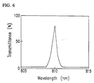
- Figure 6 is a graph showing a transmission spectrum of a thin film optical element (transmission type filter) according to the present invention.
- Figure 7 is a view showing a semiconductor-laser-excited solid laser short wavelength light source apparatus according to the present invention incorporating a thin film optical element (transmission type filter) stabilizing the oscillation wavelength of the semiconductor laser.
- Figure 8 is a view showing a semiconductor-laser-excited intracavity type short wavelength light source apparatus according to the present invention incorporating a thin film optical element (transmission type filter) stabilizing the oscillation wavelength of the semiconductor laser.
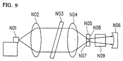
- Figure 9 is a view showing a semiconductor-laser-excited intracavity type short wavelength light source apparatus according to the present invention incorporating a thin film optical element (transmission type filter) stabilizing the oscillation wavelength of the semiconductor laser.
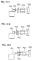
- Figure 10A is a view showing a short wavelength light source apparatus according to the present invention in which a dielectric multilayer film is provided on an outgoing end face of a semiconductor laser.
- Figure 10B is a view showing a short wavelength light source apparatus according to the present invention in which a dielectric multilayer film is provided on an incident end face of a laser medium.
- Figure 10C is a view showing a short wavelength light source apparatus according to the present invention in which a dielectric multilayer film is provided on an outgoing end face of a laser medium.
- Figure 11 is a view showing a conventional short wavelength light source apparatus incorporating a semiconductor laser and a polarization inversion type waveguide element, in which grating feedback technique is used.
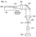
- Figure 12 is a view showing a conventional short wavelength light source apparatus incorporating a semiconductor laser and an intracavity type solid laser, in which grating feedback technique is used.
- a band-stop type (reflective type) filter including a dielectric multilayer film is used as a thin film optical element F03 in the present example.
- the thin film optical element F03 is composed essentially of a dielectric material such a SiO 2 and TiO 2 layered on a glass substrate (thickness: 0.5 mm).
- Figure 2 shows reflection characteristics of the thin film optical element F03.
- the reflectance of the thin film element F03 for light having a wavelength of 809 nm is about 10 % when the light perpendicularly enters the thin film element F03.
- Reference numeral F01 denotes a 100 mW-class single longitudinal mode semiconductor laser having an oscillation wavelength in the 810 nm band;
- F02 denotes a collimating lens (N.A.: 0.5); and
- F04 denotes a focusing lens for coupling light to a laser medium Nd:YVO 4 F05.
- Light emitted from the semiconductor laser F01 and collimated by the collimating lens F02 is led through the thin film optical element F03 , which is disposed perpendicularly to the optical axis of the semiconductor laser F01 .
- the thin film optical element F03 feeds back a portion of light having a wavelength in the vicinity of 809 nm to an active layer of the semiconductor laser F01 .
- the thin film optical element F03 has a relatively wide reflection spectrum width of about 5 nm.
- the semiconductor laser provided in the present example has a stable single longitudinal mode spectrum.
- An AR coating (reflectance R: 7%) which does not reflect the pump light (wavelength: 809 nm) emitted from the semiconductor laser F01 , and an HR coating (R > 99.9%) for reflecting light of the oscillation wavelength (1064 nm) are provided on an incident end face F07 of the Nd:YVO 4 (laser medium) F05 .
- the incident end face F07 of the Nd:YVO 4 F05 functions as a mirror for light of the oscillation wavelength (1064 nm).
- an AR coating which does not reflect light of the oscillation wavelength (1064 nm) is provided on an outgoing end face F08 of the Nd:YVO 4 F05 .
- An HR coating (R > 95%) for reflecting light of the oscillation wavelength (1064 nm) is provided on the output mirror F06 .
- a resonator for the fundamental wave of the oscillation wavelength (1064 nm) is constituted by the output mirror F06 and the incident end face F07 of the Nd:YVO 4 F05 .
- an AR coating which does not reflect light of the oscillation wavelength (1064 nm) is provided on the outgoing end face F08 of the Nd:YVO 4 F05 , and the output mirror F06 is used in the short wavelength light source apparatus of the present example.
- an HR coating R > 95%) for reflecting light of the oscillation wavelength (1064 nm) on an outgoing end face H08 of Nd:YVO 4 H05 without using the output mirror F06 .
- an imaginary output mirror is formed on the outgoing end face H08 of the Nd:YVO 4 H05 , thereby reducing the length of the resonator.
- the incident end face F07 of the Nd:YVO 4 F05 functions as an incident mirror in the present example, it is also applicable to provide a separate incident mirror.
- the thin film optical element F03 is integrally form on the incident end face F07 or the outgoing end face F08 of the Nd:YVO 4 F05 , so that the number of the component elements of the short wavelength light source apparatus is reduced, thereby facilitating further miniaturization of the short wavelength light source apparatus.
- the end faces of the Nd:YVO 4 F05 are confocally disposed with the outgoing end face of the semiconductor laser F01 . Therefore, light reflected by the thin film optical element F03 can be fed back to the semiconductor laser F01 even if the thin film optical element F03 and the optical axis are slightly shifted from a perpendicular position.
- a short wavelength light source apparatus according to a second example of the present invention will be described with reference to Figure 4 .
- the short wavelength light source apparatus of the present example incorporates an optical wavelength converting element inserted into the resonator of the short wavelength light source apparatus shown in Figure 1 .
- the oscillation wavelength of a semiconductor laser I01 is stabilized at 809 nm owing to the thin film optical element I03 , and light transmitted through the thin film optical element I03 is utilized as pump light for Nd:YVO 4 I05 .
- KTP (KTiOPO 4 ) I09 (length: 5 mm) is disposed as an optical wavelength converting element between the Nd:YVO 4 I05 and an output mirror I06 .
- Light having a wavelength of 1064 nm oscillating between an incident end face I07 of the Nd:YVO 4 I05 and the output mirror I06 is converted into green light having a wavelength of 532 nm by the KTP I09 .
- An AR coating (reflectance R: 7%) which does not reflect the pump light (wavelength: 809 nm) emitted from the semiconductor laser I01 , and an HR coating (R > 99.9%) for reflecting light of the oscillation wavelength (1064 nm) are provided on the incident end face I07 of the Nd:YVO 4 I05 .
- an AR coating which reflects neither light having a wavelength of 1064 nm nor light having a wavelength of 532 nm is provided on an outgoing end face I08 of the Nd:YVO 4 I05 .
- An HR coating for reflecting light having a wavelength of 1064 nm is provided on the output mirror I06 .
- a resonator for the fundamental wave (1064 nm) is constituted by the output mirror I06 and the incident end face I07 of the Nd:YVO 4 I05 .
- the conversion efficiency into a harmonic wave increases as the reflectance for the fundamental wave of a mirror included in the resonator increases.
- green light of about 15 mW is obtained, laser light of about 70 mW (pump power) being coupled to the Nd:YVO 4 I05 .
- Nd:YVO 4 is used as a laser medium in Examples 1 and 2 , similar effects can be obtained by using a laser material doped with Nd (such as Nd:YAG, Nd:GGG, Nd:LN, NYAB, and Nd:YLF) or a tunable laser material doped with Cr, Ti, etc.
- a laser material doped with Nd such as Nd:YAG, Nd:GGG, Nd:LN, NYAB, and Nd:YLF
- a tunable laser material doped with Cr, Ti etc.
- KTP crystal is used as an optical wavelength converting element in Example 2
- wavelength conversion can also be achieved by using other organic or inorganic non-linear optical crystals, or a polarization inversion type bulk element including a substrate composed of LiTaO 3 (LT), LiNbO 3 (LN), or KTiOPO 4 (KTP), thus providing harmonic light.
- LT LiTaO 3
- LN LiNbO 3
- KTP KTiOPO 4
- reference numeral J01 denotes a 100 mW-class single longitudinal mode semiconductor laser having an oscillation wavelength in the 810 nm band
- J02 denotes a collimating lens (N.A.: 0.5)
- J04 denotes a focusing lens for coupling light to a laser medium Nd:YVO 4 J05
- J03 denotes a thin film optical element having transmission spectrum characteristics shown in Figure 20 .
- a thin film optical element having such transmission spectrum characteristics is referred to as a band-pass type filter.
- the thin film optical element J03 is formed by laminating a few dozen layers of a dielectric material, e.g. TiO 2 , on a glass substrate having a thickness of 0.5 mm.
- the thin film optical element J03 has a transmittance of 80% for light having a wavelength of 809 nm, and a transmission spectrum half width of 1 nm.
- a peak wavelength of the transmission spectrum of a band-pass type filter generally has angle dependence.
- Figure 20 illustrates a transmission spectrum of a case where the incident light enters at an angle of 20° with the optical axis.
- the shift amount of the peak wavelength of the transmission spectrum shown in Figure 6 is 1.5 nm/deg. When the incident angle is in the vicinity of 10°, the shift amount is 0.9 nm/deg. When the incident angle is 0°, the peak wavelength makes substantially no shift depending on the angle.
- the shift amount of the transmission spectrum of the bandpass type filter (thin film optical element) J03 is not so large as compared with an angle dependence of 28 nm/deg, for example, of a grating. Therefore, the adjustment using the thin film optical element J03 is relatively easy, and the short wavelength light source apparatus is stable against temporal deterioration even if configurated as a module. Moreover, the short wavelength light source apparatus of the present example is stable against temperature changes as well (wavelength shift against temperature changes: 0.005 nm/°C). The short wavelength light source apparatus is also stable against changes in moisture.
- An AR coating (reflectance R: 7%) which does not reflect the light having a wavelength of 809 nm, and an HR coating (R > 99.9%) for reflecting light of the oscillation wavelength (1064 nm) are provided on an incident end face J07 of a laser medium Nd:YVO 4 J05 .
- an AR coating which does not reflect light of the oscillation wavelength (1064 nm) is provided on an outgoing end face J08 of the Nd:YVO 4 J05 .
- An HR coating (R > 95%) for reflecting light of the oscillation wavelength (1064 nm) is provided on an output mirror J06 .
- a resonator for the fundamental wave of the oscillation wavelength (1064 nm) is constituted by the output mirror J06 and the incident end face J07 of the Nd:YVO 4 J05 .
- the thin film optical element J03 By disposing the thin film optical element J03 between the semiconductor laser J01 and the Nd:YVO 4 J05 at an angle of 20° with the optical axis, only light having a wavelength in the vicinity of 809 nm, emitted from the semiconductor laser J01 , is incident to the incident end face J07 of the Nd:YVO 4 J05 so as to be reflected thereby, and is optically fed back to the semiconductor laser J01 .
- the semiconductor laser J01 stably oscillates in a single longitudinal mode, the oscillation wavelength thereof being stabilized in the vicinity of 809 nm.
- an AR coating is provided on the incident end face J07 of the Nd:YVO 4 J05 .
- the AR coating is designed to have the highest reflectance for the fundamental wave of 809 nm, it inevitably has a reflectance on the order of a few % for light having a wavelength in the vicinity of 809 nm, thereby causing return of (reflected) light.
- the short wavelength light source apparatus of the present example effectively utilizes the returning (reflected) light so as to stabilize the oscillation wavelength of the semiconductor laser.
- the thin film optical element J03 is disposed at a certain angle with the optical axis of the semiconductor laser J01 , as is shown in Figure 5.
- the thin film optical element J03 reflects light having wavelengths other than those in the vicinity of 809 nm.
- light having wavelengths other than those in the vicinity of 809 nm is not optically fed back to the active layer of the semiconductor laser J01 .
- the Nd:YVO 4 J05 is excited by the semiconductor laser J01 , of which oscillation wavelength is stabilized in the vicinity of 809 nm, so that the fundamental wave of 1064 nm oscillates between the incident end face J07 of the Nd:YVO 4 J05 and the output mirror J06 .
- laser light having wavelength of 1064 nm is obtained through the output mirror J06 .
- an AR coating is provided on the outgoing end face J08 of the Nd:YVO 4 J05 in the present example.
- an output mirror i.e. an HR coating (R > 95%) for reflecting light of the oscillation wavelength, on an outgoing end face L08 of a Nd:YVO 4 L05 , so as to provide a micro-chip laser having a short resonator length.
- Such a micro-chip laser is even more stable because the longitudinal mode of the fundamental wave (1064 nm) is also stabilized as a single mode.
- an incident mirror HR coating
- the resultant short wavelength light source apparatus would be similarly stable.
- a short wavelength light source apparatus can also be realized by inserting an optical wavelength converting element into the resonator shown in Figure 5.
- Figure 8 shows such a short wavelength light source apparatus.
- the oscillation wavelength of a semiconductor laser M01 is stabilized at 809 nm owing to a thin film optical element M03 , and light transmitted through the thin film optical element M03 is utilized as pump light for Nd:YVO 4 M05 .
- KTP (KTiOPO 4 ) M09 (length: 5 mm) is disposed as an optical wavelength converting element between Nd:YVO 4 M05 and an output mirror M06 .
- Light having a wavelength of 1064 nm oscillating between an incident end face M07 of the Nd:YVO 4 M05 and the output mirror M06 is converted into green light having a wavelength of 532 nm by the KTP M09 .
- An AR coating (reflectance R: 7%) which does not reflect the pump light (wavelength: 809 nm) emitted from the semiconductor laser M01 , and an HR coating (R > 99.9%) for reflecting light of the oscillation wavelength (1064 nm) and harmonic light (532 nm) are provided on the incident end face M07 of the Nd:YVO 4 M05 .
- an AR coating which reflects neither light having a wavelength of 1064 nm nor light having a wavelength of 532 nm is provided on an outgoing end face M08 of the Nd:YVO 4 M05 .
- An HR coating for reflecting light having a wavelength of 1064 nm is provided on the output mirror M06 .
- a resonator for the fundamental wave (1064 nm) is constituted by the output mirror M06 and the incident end face M07 of the Nd:YVO 4 M05 .
- the conversion efficiency into a harmonic wave increases as the reflectance for the fundamental wave of a mirror included in the resonator increases.
- green light of about 15 mW is obtained, laser light of about 70 mW (pump power) being coupled to the Nd:YVO 4 M05 .
- Nd:YVO 4 is used as a laser medium in Examples 4 and 5 , similar effects can be obtained by using a laser material doped with Nd (such as Nd:YAG, Nd:GGG, Nd:LN, NYAB, and Nd:YLF) or a tunable laser material doped with Cr, Ti, etc.
- a laser material doped with Nd such as Nd:YAG, Nd:GGG, Nd:LN, NYAB, and Nd:YLF
- a tunable laser material doped with Cr, Ti etc.
- KTP crystal is used as an optical wavelength converting element in Example 5
- wavelength conversion can also be achieved by using other organic or inorganic non-linear optical crystals, or a polarization inversion type bulk element including a substrate composed of LiTaO 3 (LT), LiNbO 3 (LN), or KTiOPO 4 (KTP), thus providing harmonic light.
- LT LiTaO 3
- LN LiNbO 3
- KTP KTiOPO 4
- the stabilization of the oscillation wavelength of the semiconductor laser is achieved by optically feeding back returning light which is reflected by the incident end face of the laser medium Nd:YVO 4 to the semiconductor laser.
- the oscillation wavelength can also be stabilized by providing an HR coating (preferably R > 95%) for reflecting light having a wavelength of 809 nm on the outgoing end face of the semiconductor laser so as to feed back light which is not absorbed by the laser oscillation material to the semiconductor laser.
- a thickness of about 1 mm is usually selected for the material; in the case of a material consisting of YVO 4 doped with 2% Nd, a thickness of about 0.5 mm is usually selected for the material; in the case of a material consisting of YVO 4 doped with 3% Nd, a thickness of about 0.3 mm is usually selected for the material.
- the Nd:YVO 4 N05 must have a thickness smaller than is considered proper.
- the oscillated laser light is absorbed by a material consisting of YVO 4 doped with 1% Nd which has a thickness of 0.5 mm, so that a few % of the light is fed back to the semiconductor laser N01 .
- a thin film optical element N09 is a band-pass type filter identical with that shown in Figure 5 (which has the transmission spectrum characteristics shown in Figure 6 ).
- a thin film optical element N03 shown in Figure 9 can alternatively be disposed on an incident end face N07 of the Nd:YVO 4 N05 .
- only light having a wavelength in the vicinity of 809 nm reflected by the outgoing end face N08 of the Nd:YVO 4 N05 is fed back to the active layer of the semiconductor laser N01 , whereby stable excitation of the laser medium Nd:YVO 4 N05 is achieved.
- Stabilization of the oscillation wavelength of a semiconductor laser P01, stable wavelength conversion, and high harmonic output power can be provided by: providing a transmission type filter composed essentially of a dielectric multilayer film P02 on an outgoing end face of the semiconductor laser P01 (as is shown in Figure 10A); or providing a transmission type (band-pass-type) or reflective type (band-stop type) filter composed essentially of a dielectric multilayer film on an incident end face (as is shown in Figure 10B) or on an outgoing end face (as is shown in Figure 10C) of Nd:YVO 4 P03.
- a reflective type filter (thin film optical element) identical with that shown in Figure 1 is provided on the incident end face of the Nd:YVO 4 P03 is disposed perpendicularly to the optical axis of the semiconductor laser P01.
- a transmission type filter is provided on the incident end face of the Nd:YVO 4 P03 , instead of the reflective type filter, light reflected by the outgoing end face of the Nd:YVO 4 P03 is utilized as light fed back to the semiconductor laser P01.
- a reflective type filter (thin film optical element) is provided on the outgoing end face of the Nd:YVO 4 P03, and an optical system is omitted.
- the semiconductor laser P01 is disposed at a distance of 10 ⁇ m from the Nd:YVO 4 P03.
- the Nd:YVO 4 P03 is disposed perpendicularly to the optical axis of the semiconductor laser P01.
- the oscillation wavelength of a semiconductor laser of a short wavelength light source apparatus can also be stabilized by using a Bragg's reflective type thin film optical element composed essentially of a plurality of periodically formed layers as a reflective type filter.
- a method for producing a Bragg's reflective type thin film optical element will be described.
- SiO 2 (refractive index: 1.46), SiO 2 having a different composition (refractive index: 1.48) are alternately formed with a period of 0.27 ⁇ m on a quartz substrate by means of an EB vapor deposition apparatus.
- About 100 such layers are laminated to form the Bragg's reflective type thin film optical element.
- a Bragg's reflective type thin film optical element is very practical because the spectrum width thereof can be easily adjusted by varying the number of the layers laminated.
- the oscillation wavelength of a semiconductor laser of a short wavelength light source apparatus incorporating this Braggs's reflective type thin film optical element instead of a band-stop filter is stabilized at the phase matching wavelength or the absorption wavelength. Stable green/blue light is obtained without any mode hopping.
- a Bragg's reflective type filter can also be realized by a holographical method where laser light of a predetermined wavelength is incident to a photorefractive material such as LT and LN doped with Fe in two directions so that the two laser light beams interfere with each other.
- a band-pass type interference filter is capable of achieving a transmittance of about 100% as long as the transmission spectrum width is on the order of a few nm (nanometers).
- Using a filter having a broad transmission spectrum width for stabilization of the oscillation wavelength would broaden the spectrum width of the semiconductor laser, that is, the semiconductor laser would have a multitude of modes.
- using such a filter with a broad transmission spectrum width is appropriate for high-efficiency excitation because the laser oscillation material has an absorption spectrum width of about a few nm, whereby highly efficient excitation is achieved and the output power of the semiconductor laser can be effectively utilized.
- Each of the transmission type or reflective type filters shown in Figures 1 , 3 , 4 , 5, 7, 8 , and 9 is a thin film optical element obtained by forming a dielectric multilayer film on a glass substrate having a thickness of 0.5 mm. It has been found out that the oscillation wavelength becomes especially stable when the glass substrate has a thickness in the range of 0.2 mm to 2.0 mm. The oscillation wavelength becomes unstable when the thickness of the substrate is 0.2 mm or less because of the warping of the substrate after polishing. The oscillation wavelength has an aberration when the thickness of the substrate is 2.0 mm or more owing to the thickness of the substrate.
- a thin film optical element including a dielectric multilayer film formed on a glass substrate is used as an optical element for transmitting or reflecting light in a predetermined wavelength band.
- the longitudinal mode of the semiconductor laser can also be locked and stabilized by using the following as an optical element: an etalon element including a highly planar element polished so as to be highly planar and so as to have a high degree of parallelism and a reflective film formed on each side of the highly planar element; or a birefringence filter that utilizes interference between normal light and extraordinary light in a birefringence crystal plate.
- Etalon composed of synthetic quartz having a thickness of 50 ⁇ m, a reflectance of 85%, and a parallelism of ⁇ /10 is used in the present example.
- Etalon has peak transmittances at certain intervals when transmittance is regarded as a function of the wavelength of incident light.
- finesse F of the etalon is derived.
- the finesse F is expressed as a ratio between ⁇ v and the half width ⁇ v 1/2 of a certain mode.
- the reflection finesse F r 2 and the planarity finesse F d 2 are expressed by the following equations: :Eq. 3
- F r 2 ⁇ 2 R/ (1 - R) 2 :Eq.
- the value 1 nm of the half width of the etalon of the present example is substantially the same as that of a transmission type filter (thin film optical element).
- An interference pattern can be obtained by radiating light on a crystal panel interposed between two polarizing plates, corresponding to the change in the wavelength of the incident light.
- the interference patterns overlap with one another so that a sharp peak is left.
- a band-pass filter having a transmission spectrum width of about 0.1 nm is realized.
- the oscillation wavelength of the semiconductor laser can be stabilized also by using such a birefringence filter in the place of a thin film optical element.
- a compact, stable, and high-power short wavelength light source apparatus for generating green or blue light which incorporates as a pump light source a light generating device including an optical element for transmitting or reflecting light in a predetermined wavelength band, and a polarization inversion type waveguide element, a polarization inversion type bulk element, and/or a non-linear optical crystal for converting light emitted from the semiconductor laser into light having a different wavelength.
- a short wavelength light source apparatus according to the present invention is also capable of providing near infrared light by incorporating a laser medium, and providing stable short wavelength light by adopting an intracavity configuration.
- the present invention has a large practical significance because it can provide a short wavelength light source apparatus to be used for an optical disk or for measurement purposes, where the short wavelength light source apparatus is required to have a stable, low-noise output power.
- a short wavelength light source apparatus incorporating a semiconductor laser is likely to have the problem of unstable oscillation by the semiconductor laser due to light returning from an end face of an optical wavelength converting element or an end face of a laser medium.
- the optical component elements can be linearly disposed, thereby facilitating miniaturization of the short wavelength light source apparatus.
- a peak wavelength of the transmission spectrum of a transmission type filter generally has angle dependence.
- the peak wavelength of the transmission spectrum shifts by 1.5 nm/deg.
- the shift amount is 0.9 nm/deg.
- the peak wavelength makes substantially no shift depending on the angle.
- the oscillation wavelength of the semiconductor laser can be tuned to be the phase matching wavelength of the optical wavelength converting element.
- the shift amount of the transmission spectrum of a transmission filter is not so large as compared with that of a grating, e.g. 28 nm/deg.
- a transmission type filter to stabilize the oscillation wavelength of the semiconductor laser makes the necessary optical adjustment easier than using grating feedback technique. It will be appreciated that use of a transmission type filter (thin film optical element) for stabilization of the oscillation wavelength of the semiconductor laser has great practical effects.
- a short wavelength light source apparatus is stable against temperature changes, having a wavelength shift of 0.005 nm/°C, and is also stable against changes in moisture. Since it is not composed of resin unlike a grating, the entire short wavelength light source apparatus is made reliable.
- oscillation wavelength locking Even more stable oscillation wavelength (oscillation wavelength locking) can be achieved by incorporating an etalon or a birefringence filter, since the half width of the transmission spectrum of such elements can be reduced to about 0.1 nm.
Applications Claiming Priority (10)
| Application Number | Priority Date | Filing Date | Title |
|---|---|---|---|
| JP119742/93 | 1993-05-21 | ||
| JP11974293 | 1993-05-21 | ||
| JP11974293 | 1993-05-21 | ||
| JP24652993 | 1993-10-01 | ||
| JP246529/93 | 1993-10-01 | ||
| JP24652993 | 1993-10-01 | ||
| JP247883/93 | 1993-10-04 | ||
| JP24788393 | 1993-10-04 | ||
| JP24788393 | 1993-10-04 | ||
| EP94107841A EP0625811B1 (de) | 1993-05-21 | 1994-05-20 | Vorrichtung mit kurzwellenlängiger Lichtquelle |
Related Parent Applications (2)
| Application Number | Title | Priority Date | Filing Date |
|---|---|---|---|
| EP94107841.2 Division | 1994-05-20 | ||
| EP94107841A Division EP0625811B1 (de) | 1993-05-21 | 1994-05-20 | Vorrichtung mit kurzwellenlängiger Lichtquelle |
Publications (3)
| Publication Number | Publication Date |
|---|---|
| EP0738031A2 true EP0738031A2 (de) | 1996-10-16 |
| EP0738031A3 EP0738031A3 (de) | 1997-06-04 |
| EP0738031B1 EP0738031B1 (de) | 2001-07-18 |
Family
ID=27313896
Family Applications (2)
| Application Number | Title | Priority Date | Filing Date |
|---|---|---|---|
| EP96110043A Expired - Lifetime EP0738031B1 (de) | 1993-05-21 | 1994-05-20 | Vorrichtung mit kurzwelliger Lichtquelle |
| EP94107841A Expired - Lifetime EP0625811B1 (de) | 1993-05-21 | 1994-05-20 | Vorrichtung mit kurzwellenlängiger Lichtquelle |
Family Applications After (1)
| Application Number | Title | Priority Date | Filing Date |
|---|---|---|---|
| EP94107841A Expired - Lifetime EP0625811B1 (de) | 1993-05-21 | 1994-05-20 | Vorrichtung mit kurzwellenlängiger Lichtquelle |
Country Status (2)
| Country | Link |
|---|---|
| EP (2) | EP0738031B1 (de) |
| DE (2) | DE69423022T2 (de) |
Cited By (3)
| Publication number | Priority date | Publication date | Assignee | Title |
|---|---|---|---|---|
| WO2009014663A1 (en) * | 2007-07-20 | 2009-01-29 | Corning Incorporated | Intensity modulation in wavelength converting optical package |
| US7586971B2 (en) | 2006-12-26 | 2009-09-08 | Seiko Epson Corporation | External-cavity laser light source apparatus and laser light emission module |
| US9762022B2 (en) | 2013-12-05 | 2017-09-12 | Mitsubishi Electric Corporation | Multi wavelength laser device |
Families Citing this family (9)
| Publication number | Priority date | Publication date | Assignee | Title |
|---|---|---|---|---|
| US5640405A (en) * | 1996-02-01 | 1997-06-17 | Lighthouse Electronics Corporation | Multi quasi phase matched interactions in a non-linear crystal |
| EP1875566B1 (de) * | 2005-03-30 | 2014-05-21 | Necsel Intellectual Property, Inc. | Frequenzstabilisierte oberflächenemissionslaser mit erweitertem resonator |
| WO2006112412A1 (ja) | 2005-04-15 | 2006-10-26 | Sumitomo Osaka Cement Co., Ltd. | レーザ光発生装置および発生方法 |
| CN101233657A (zh) | 2005-07-28 | 2008-07-30 | 松下电器产业株式会社 | 激光光源和显示器装置 |
| ATE514210T1 (de) * | 2007-07-05 | 2011-07-15 | Koninkl Philips Electronics Nv | Oberflächenemittierendes lasergerät mit externem resonator |
| US8111452B2 (en) | 2010-02-22 | 2012-02-07 | Corning Incorporated | Wavelength conversion device with microlens and optical package incorporating the same |
| US8942267B2 (en) | 2011-05-17 | 2015-01-27 | Redshift Systems Corporation | Thermo-optically tunable laser system |
| WO2017205833A1 (en) * | 2016-05-26 | 2017-11-30 | Compound Photonics Ltd | Solid-state laser system |
| US20190245319A1 (en) * | 2016-05-26 | 2019-08-08 | Compound Photonics Limited | Solid-state laser system |
Citations (1)
| Publication number | Priority date | Publication date | Assignee | Title |
|---|---|---|---|---|
| EP0559139A1 (de) * | 1992-03-03 | 1993-09-08 | Matsushita Electric Industrial Co., Ltd. | Vorrichtung zur Erzeugung von Licht mit kurzer Wellenlänge |
Family Cites Families (4)
| Publication number | Priority date | Publication date | Assignee | Title |
|---|---|---|---|---|
| JPH01257922A (ja) * | 1988-04-08 | 1989-10-16 | Nec Corp | 導波路型波長変換素子 |
| JP2718259B2 (ja) * | 1990-11-06 | 1998-02-25 | 松下電器産業株式会社 | 短波長レーザ光源 |
| JPH0566440A (ja) * | 1991-02-13 | 1993-03-19 | Matsushita Electric Ind Co Ltd | レーザ光源 |
| US5185752A (en) * | 1992-02-18 | 1993-02-09 | Spectra Diode Laboratories, Inc. | Coupling arrangements for frequency-doubled diode lasers |
-
1994
- 1994-05-20 EP EP96110043A patent/EP0738031B1/de not_active Expired - Lifetime
- 1994-05-20 DE DE69423022T patent/DE69423022T2/de not_active Expired - Lifetime
- 1994-05-20 DE DE69427771T patent/DE69427771T2/de not_active Expired - Lifetime
- 1994-05-20 EP EP94107841A patent/EP0625811B1/de not_active Expired - Lifetime
Patent Citations (1)
| Publication number | Priority date | Publication date | Assignee | Title |
|---|---|---|---|---|
| EP0559139A1 (de) * | 1992-03-03 | 1993-09-08 | Matsushita Electric Industrial Co., Ltd. | Vorrichtung zur Erzeugung von Licht mit kurzer Wellenlänge |
Non-Patent Citations (3)
| Title |
|---|
| APPLIED PHYSICS LETTERS, 19 JULY 1993, USA, vol. 63, no. 3, ISSN 0003-6951, pages 299-301, XP000382577 KITAOKA Y ET AL: "Stable and efficient green light generation by intracavity frequency doubling of Nd:YVO/sub 4/ lasers" * |
| OPTICS LETTERS, 1 JAN. 1993, USA, vol. 18, no. 1, ISSN 0146-9592, pages 34-36, XP000328271 STEPHENS R R ET AL: "Diode-pumped upconversion laser with 100 mW output power" * |
| OPTICS LETTERS, OCT. 1988, USA, vol. 13, no. 10, ISSN 0146-9592, pages 826-828, XP000050989 ZORABEDIAN P ET AL: "Interference-filter-tuned, alignment-stabilized, semiconductor external-cavity laser" * |
Cited By (4)
| Publication number | Priority date | Publication date | Assignee | Title |
|---|---|---|---|---|
| US7586971B2 (en) | 2006-12-26 | 2009-09-08 | Seiko Epson Corporation | External-cavity laser light source apparatus and laser light emission module |
| WO2009014663A1 (en) * | 2007-07-20 | 2009-01-29 | Corning Incorporated | Intensity modulation in wavelength converting optical package |
| US7782913B2 (en) | 2007-07-20 | 2010-08-24 | Corning Incorporated | Intensity modulation in wavelength converting optical package |
| US9762022B2 (en) | 2013-12-05 | 2017-09-12 | Mitsubishi Electric Corporation | Multi wavelength laser device |
Also Published As
| Publication number | Publication date |
|---|---|
| EP0738031B1 (de) | 2001-07-18 |
| EP0625811A1 (de) | 1994-11-23 |
| DE69427771D1 (de) | 2001-08-23 |
| DE69423022D1 (de) | 2000-03-23 |
| DE69423022T2 (de) | 2000-08-03 |
| EP0738031A3 (de) | 1997-06-04 |
| DE69427771T2 (de) | 2004-10-14 |
| EP0625811B1 (de) | 2000-02-16 |
Similar Documents
| Publication | Publication Date | Title |
|---|---|---|
| US5809048A (en) | Wavelength stabilized light source | |
| US5265116A (en) | Microchip laser | |
| US5402437A (en) | Microchip laser | |
| US4953166A (en) | Microchip laser | |
| US5377212A (en) | Solid-state laser device including uniaxial laser crystal emitting linearly polarized fundamental wave and nonlinear optical crystal emitting linearly polarized harmonic wave | |
| EP0738031B1 (de) | Vorrichtung mit kurzwelliger Lichtquelle | |
| US7173950B2 (en) | Low-noise high-power SHG laser system | |
| US5227911A (en) | Monolithic total internal reflection optical resonator | |
| JP3222340B2 (ja) | 単一縦モードレーザー | |
| US5341393A (en) | Laser-diode-pumped solid-state laser | |
| JPH07152055A (ja) | 短波長光源および波長可変レーザ光源 | |
| JPH1093182A (ja) | 周波数変換型固体レーザ装置、周波数2倍型固体レーザ装置および周波数変換型結合型共振キャビティ | |
| JP3683360B2 (ja) | 偏光制御素子および固体レーザー | |
| US5502738A (en) | Polarization control element and solid-state laser system | |
| Kean et al. | Generation of 20 mW of blue laser radiation from a diode‐pumped sum‐frequency laser | |
| JP3786878B2 (ja) | レーザ光源 | |
| EP0820130B1 (de) | Vorrichtung zur Emission eines Laserstrahls | |
| JPH08213686A (ja) | 波長安定化光源 | |
| US7471707B2 (en) | Low noise, intra-cavity frequency-doubling micro chip laser with wide temperature range | |
| EP0748008B1 (de) | Laser und Verwendungen | |
| US20100220753A1 (en) | Monofrequency intra-cavity frequency-tripled continuous laser | |
| JPH0728111A (ja) | 回折素子および光波長変換素子ならびにレーザ光源 | |
| JPH09331097A (ja) | 固体レーザ装置 | |
| KR100366699B1 (ko) | 내부 공진형 제2 고조파 발생 장치 | |
| JPH03108785A (ja) | レーザ光波長変換方式 |
Legal Events
| Date | Code | Title | Description |
|---|---|---|---|
| PUAI | Public reference made under article 153(3) epc to a published international application that has entered the european phase |
Free format text: ORIGINAL CODE: 0009012 |
|
| 17P | Request for examination filed |
Effective date: 19960621 |
|
| AC | Divisional application: reference to earlier application |
Ref document number: 625811 Country of ref document: EP |
|
| AK | Designated contracting states |
Kind code of ref document: A2 Designated state(s): DE FR |
|
| RAP1 | Party data changed (applicant data changed or rights of an application transferred) |
Owner name: MATSUSHITA ELECTRIC INDUSTRIAL CO., LTD. |
|
| PUAL | Search report despatched |
Free format text: ORIGINAL CODE: 0009013 |
|
| AK | Designated contracting states |
Kind code of ref document: A3 Designated state(s): DE FR |
|
| 17Q | First examination report despatched |
Effective date: 19990630 |
|
| RTI1 | Title (correction) |
Free format text: A SHORT WAVELENGTH LIGHT SOURCE APPARATUS |
|
| GRAG | Despatch of communication of intention to grant |
Free format text: ORIGINAL CODE: EPIDOS AGRA |
|
| GRAG | Despatch of communication of intention to grant |
Free format text: ORIGINAL CODE: EPIDOS AGRA |
|
| GRAH | Despatch of communication of intention to grant a patent |
Free format text: ORIGINAL CODE: EPIDOS IGRA |
|
| GRAH | Despatch of communication of intention to grant a patent |
Free format text: ORIGINAL CODE: EPIDOS IGRA |
|
| GRAA | (expected) grant |
Free format text: ORIGINAL CODE: 0009210 |
|
| AC | Divisional application: reference to earlier application |
Ref document number: 625811 Country of ref document: EP |
|
| AK | Designated contracting states |
Kind code of ref document: B1 Designated state(s): DE FR |
|
| REF | Corresponds to: |
Ref document number: 69427771 Country of ref document: DE Date of ref document: 20010823 |
|
| ET | Fr: translation filed | ||
| PLBE | No opposition filed within time limit |
Free format text: ORIGINAL CODE: 0009261 |
|
| STAA | Information on the status of an ep patent application or granted ep patent |
Free format text: STATUS: NO OPPOSITION FILED WITHIN TIME LIMIT |
|
| 26N | No opposition filed | ||
| REG | Reference to a national code |
Ref country code: DE Ref legal event code: R084 Ref document number: 69427771 Country of ref document: DE Effective date: 20111010 |
|
| PGFP | Annual fee paid to national office [announced via postgrant information from national office to epo] |
Ref country code: FR Payment date: 20120608 Year of fee payment: 19 |
|
| PGFP | Annual fee paid to national office [announced via postgrant information from national office to epo] |
Ref country code: DE Payment date: 20120516 Year of fee payment: 19 |
|
| PG25 | Lapsed in a contracting state [announced via postgrant information from national office to epo] |
Ref country code: DE Free format text: LAPSE BECAUSE OF NON-PAYMENT OF DUE FEES Effective date: 20131203 |
|
| REG | Reference to a national code |
Ref country code: DE Ref legal event code: R119 Ref document number: 69427771 Country of ref document: DE Effective date: 20131203 |
|
| REG | Reference to a national code |
Ref country code: FR Ref legal event code: ST Effective date: 20140131 |
|
| PG25 | Lapsed in a contracting state [announced via postgrant information from national office to epo] |
Ref country code: FR Free format text: LAPSE BECAUSE OF NON-PAYMENT OF DUE FEES Effective date: 20130531 |