EP0625811A1 - Vorrichtung mit kurzwellenlängiger Lichtquelle - Google Patents
Vorrichtung mit kurzwellenlängiger Lichtquelle Download PDFInfo
- Publication number
- EP0625811A1 EP0625811A1 EP94107841A EP94107841A EP0625811A1 EP 0625811 A1 EP0625811 A1 EP 0625811A1 EP 94107841 A EP94107841 A EP 94107841A EP 94107841 A EP94107841 A EP 94107841A EP 0625811 A1 EP0625811 A1 EP 0625811A1
- Authority
- EP
- European Patent Office
- Prior art keywords
- optical
- wavelength
- light source
- source apparatus
- short wavelength
- Prior art date
- Legal status (The legal status is an assumption and is not a legal conclusion. Google has not performed a legal analysis and makes no representation as to the accuracy of the status listed.)
- Granted
Links
Images


Classifications
-
- H—ELECTRICITY
- H01—ELECTRIC ELEMENTS
- H01S—DEVICES USING THE PROCESS OF LIGHT AMPLIFICATION BY STIMULATED EMISSION OF RADIATION [LASER] TO AMPLIFY OR GENERATE LIGHT; DEVICES USING STIMULATED EMISSION OF ELECTROMAGNETIC RADIATION IN WAVE RANGES OTHER THAN OPTICAL
- H01S3/00—Lasers, i.e. devices using stimulated emission of electromagnetic radiation in the infrared, visible or ultraviolet wave range
- H01S3/09—Processes or apparatus for excitation, e.g. pumping
- H01S3/091—Processes or apparatus for excitation, e.g. pumping using optical pumping
- H01S3/094—Processes or apparatus for excitation, e.g. pumping using optical pumping by coherent light
- H01S3/0941—Processes or apparatus for excitation, e.g. pumping using optical pumping by coherent light of a laser diode
- H01S3/09415—Processes or apparatus for excitation, e.g. pumping using optical pumping by coherent light of a laser diode the pumping beam being parallel to the lasing mode of the pumped medium, e.g. end-pumping
-
- H—ELECTRICITY
- H01—ELECTRIC ELEMENTS
- H01S—DEVICES USING THE PROCESS OF LIGHT AMPLIFICATION BY STIMULATED EMISSION OF RADIATION [LASER] TO AMPLIFY OR GENERATE LIGHT; DEVICES USING STIMULATED EMISSION OF ELECTROMAGNETIC RADIATION IN WAVE RANGES OTHER THAN OPTICAL
- H01S3/00—Lasers, i.e. devices using stimulated emission of electromagnetic radiation in the infrared, visible or ultraviolet wave range
- H01S3/10—Controlling the intensity, frequency, phase, polarisation or direction of the emitted radiation, e.g. switching, gating, modulating or demodulating
- H01S3/106—Controlling the intensity, frequency, phase, polarisation or direction of the emitted radiation, e.g. switching, gating, modulating or demodulating by controlling devices placed within the cavity
- H01S3/108—Controlling the intensity, frequency, phase, polarisation or direction of the emitted radiation, e.g. switching, gating, modulating or demodulating by controlling devices placed within the cavity using non-linear optical devices, e.g. exhibiting Brillouin or Raman scattering
- H01S3/109—Frequency multiplication, e.g. harmonic generation
-
- G—PHYSICS
- G02—OPTICS
- G02F—OPTICAL DEVICES OR ARRANGEMENTS FOR THE CONTROL OF LIGHT BY MODIFICATION OF THE OPTICAL PROPERTIES OF THE MEDIA OF THE ELEMENTS INVOLVED THEREIN; NON-LINEAR OPTICS; FREQUENCY-CHANGING OF LIGHT; OPTICAL LOGIC ELEMENTS; OPTICAL ANALOGUE/DIGITAL CONVERTERS
- G02F1/00—Devices or arrangements for the control of the intensity, colour, phase, polarisation or direction of light arriving from an independent light source, e.g. switching, gating or modulating; Non-linear optics
- G02F1/35—Non-linear optics
- G02F1/353—Frequency conversion, i.e. wherein a light beam is generated with frequency components different from those of the incident light beams
- G02F1/3544—Particular phase matching techniques
- G02F1/3548—Quasi phase matching [QPM], e.g. using a periodic domain inverted structure
-
- G—PHYSICS
- G02—OPTICS
- G02F—OPTICAL DEVICES OR ARRANGEMENTS FOR THE CONTROL OF LIGHT BY MODIFICATION OF THE OPTICAL PROPERTIES OF THE MEDIA OF THE ELEMENTS INVOLVED THEREIN; NON-LINEAR OPTICS; FREQUENCY-CHANGING OF LIGHT; OPTICAL LOGIC ELEMENTS; OPTICAL ANALOGUE/DIGITAL CONVERTERS
- G02F1/00—Devices or arrangements for the control of the intensity, colour, phase, polarisation or direction of light arriving from an independent light source, e.g. switching, gating or modulating; Non-linear optics
- G02F1/35—Non-linear optics
- G02F1/37—Non-linear optics for second-harmonic generation
- G02F1/377—Non-linear optics for second-harmonic generation in an optical waveguide structure
-
- H—ELECTRICITY
- H01—ELECTRIC ELEMENTS
- H01S—DEVICES USING THE PROCESS OF LIGHT AMPLIFICATION BY STIMULATED EMISSION OF RADIATION [LASER] TO AMPLIFY OR GENERATE LIGHT; DEVICES USING STIMULATED EMISSION OF ELECTROMAGNETIC RADIATION IN WAVE RANGES OTHER THAN OPTICAL
- H01S3/00—Lasers, i.e. devices using stimulated emission of electromagnetic radiation in the infrared, visible or ultraviolet wave range
- H01S3/005—Optical devices external to the laser cavity, specially adapted for lasers, e.g. for homogenisation of the beam or for manipulating laser pulses, e.g. pulse shaping
-
- H—ELECTRICITY
- H01—ELECTRIC ELEMENTS
- H01S—DEVICES USING THE PROCESS OF LIGHT AMPLIFICATION BY STIMULATED EMISSION OF RADIATION [LASER] TO AMPLIFY OR GENERATE LIGHT; DEVICES USING STIMULATED EMISSION OF ELECTROMAGNETIC RADIATION IN WAVE RANGES OTHER THAN OPTICAL
- H01S3/00—Lasers, i.e. devices using stimulated emission of electromagnetic radiation in the infrared, visible or ultraviolet wave range
- H01S3/05—Construction or shape of optical resonators; Accommodation of active medium therein; Shape of active medium
- H01S3/08—Construction or shape of optical resonators or components thereof
- H01S3/08018—Mode suppression
- H01S3/08022—Longitudinal modes
- H01S3/08031—Single-mode emission
-
- H—ELECTRICITY
- H01—ELECTRIC ELEMENTS
- H01S—DEVICES USING THE PROCESS OF LIGHT AMPLIFICATION BY STIMULATED EMISSION OF RADIATION [LASER] TO AMPLIFY OR GENERATE LIGHT; DEVICES USING STIMULATED EMISSION OF ELECTROMAGNETIC RADIATION IN WAVE RANGES OTHER THAN OPTICAL
- H01S3/00—Lasers, i.e. devices using stimulated emission of electromagnetic radiation in the infrared, visible or ultraviolet wave range
- H01S3/09—Processes or apparatus for excitation, e.g. pumping
- H01S3/091—Processes or apparatus for excitation, e.g. pumping using optical pumping
- H01S3/094—Processes or apparatus for excitation, e.g. pumping using optical pumping by coherent light
- H01S3/094065—Single-mode pumping
-
- H—ELECTRICITY
- H01—ELECTRIC ELEMENTS
- H01S—DEVICES USING THE PROCESS OF LIGHT AMPLIFICATION BY STIMULATED EMISSION OF RADIATION [LASER] TO AMPLIFY OR GENERATE LIGHT; DEVICES USING STIMULATED EMISSION OF ELECTROMAGNETIC RADIATION IN WAVE RANGES OTHER THAN OPTICAL
- H01S3/00—Lasers, i.e. devices using stimulated emission of electromagnetic radiation in the infrared, visible or ultraviolet wave range
- H01S3/14—Lasers, i.e. devices using stimulated emission of electromagnetic radiation in the infrared, visible or ultraviolet wave range characterised by the material used as the active medium
- H01S3/16—Solid materials
- H01S3/1601—Solid materials characterised by an active (lasing) ion
- H01S3/1603—Solid materials characterised by an active (lasing) ion rare earth
- H01S3/1611—Solid materials characterised by an active (lasing) ion rare earth neodymium
-
- H—ELECTRICITY
- H01—ELECTRIC ELEMENTS
- H01S—DEVICES USING THE PROCESS OF LIGHT AMPLIFICATION BY STIMULATED EMISSION OF RADIATION [LASER] TO AMPLIFY OR GENERATE LIGHT; DEVICES USING STIMULATED EMISSION OF ELECTROMAGNETIC RADIATION IN WAVE RANGES OTHER THAN OPTICAL
- H01S3/00—Lasers, i.e. devices using stimulated emission of electromagnetic radiation in the infrared, visible or ultraviolet wave range
- H01S3/14—Lasers, i.e. devices using stimulated emission of electromagnetic radiation in the infrared, visible or ultraviolet wave range characterised by the material used as the active medium
- H01S3/16—Solid materials
- H01S3/163—Solid materials characterised by a crystal matrix
- H01S3/1671—Solid materials characterised by a crystal matrix vanadate, niobate, tantalate
- H01S3/1673—YVO4 [YVO]
-
- H—ELECTRICITY
- H01—ELECTRIC ELEMENTS
- H01S—DEVICES USING THE PROCESS OF LIGHT AMPLIFICATION BY STIMULATED EMISSION OF RADIATION [LASER] TO AMPLIFY OR GENERATE LIGHT; DEVICES USING STIMULATED EMISSION OF ELECTROMAGNETIC RADIATION IN WAVE RANGES OTHER THAN OPTICAL
- H01S5/00—Semiconductor lasers
- H01S5/005—Optical components external to the laser cavity, specially adapted therefor, e.g. for homogenisation or merging of the beams or for manipulating laser pulses, e.g. pulse shaping
- H01S5/0092—Optical components external to the laser cavity, specially adapted therefor, e.g. for homogenisation or merging of the beams or for manipulating laser pulses, e.g. pulse shaping for nonlinear frequency conversion, e.g. second harmonic generation [SHG] or sum- or difference-frequency generation outside the laser cavity
-
- H—ELECTRICITY
- H01—ELECTRIC ELEMENTS
- H01S—DEVICES USING THE PROCESS OF LIGHT AMPLIFICATION BY STIMULATED EMISSION OF RADIATION [LASER] TO AMPLIFY OR GENERATE LIGHT; DEVICES USING STIMULATED EMISSION OF ELECTROMAGNETIC RADIATION IN WAVE RANGES OTHER THAN OPTICAL
- H01S5/00—Semiconductor lasers
- H01S5/06—Arrangements for controlling the laser output parameters, e.g. by operating on the active medium
- H01S5/065—Mode locking; Mode suppression; Mode selection ; Self pulsating
-
- H—ELECTRICITY
- H01—ELECTRIC ELEMENTS
- H01S—DEVICES USING THE PROCESS OF LIGHT AMPLIFICATION BY STIMULATED EMISSION OF RADIATION [LASER] TO AMPLIFY OR GENERATE LIGHT; DEVICES USING STIMULATED EMISSION OF ELECTROMAGNETIC RADIATION IN WAVE RANGES OTHER THAN OPTICAL
- H01S5/00—Semiconductor lasers
- H01S5/10—Construction or shape of the optical resonator, e.g. extended or external cavity, coupled cavities, bent-guide, varying width, thickness or composition of the active region
- H01S5/14—External cavity lasers
- H01S5/141—External cavity lasers using a wavelength selective device, e.g. a grating or etalon
Definitions
- the present invention relates to a light source apparatus for use in a high-density optical disk system and the like, and particularly to a short wavelength light source apparatus incorporating a semiconductor laser as a pump light source.
- a method for directly converting the wavelength of semiconductor laser light is regarded as promising.
- the method typically uses, as an optical wavelength converting element, a polarization inversion type optical waveguide element of a quasi-phase matching (hereinafter referred to as "QPM") type using LiTaO3, LiNbO3, and KTiOPO4 as a substrate (Yamamoto et al.; Optics Letters Vol.16, No.15, 1156 (1991)), a polarization inversion type bulk element, and/or a phase matching type non-linear optical crystal having a large non-linear optical constant, e.g. KNbO3(KN).
- QPM quasi-phase matching
- a laser medium receives laser light generated by a semiconductor laser (pump light source) so as to effect laser oscillation, and generates laser light having a longer wavelength than that of the laser light from the semiconductor laser.
- the generated laser light is converted into short-wavelength light (harmonics) by an optical wavelength converting element inserted in the interior of a resonator.
- the output of the QPM polarization inversion type waveguide element can be stable for a time period of only several seconds.
- Phase matching type non-linear optical crystals and QPM polarization inversion type bulk elements similarly have a relatively narrow range of allowable wavelength variation with respect to phase matching. This increases the importance of stabilization of the oscillation wavelength of a semiconductor laser used as a pump light source.
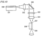
- reference numeral D01 denotes a 50 mW-class AlGaAs semiconductor laser for the 0.83 ⁇ m band
- D02 denotes a collimating lens
- D03 denotes a ⁇ /2 plate
- D04 denotes a focusing lens having a numerical aperture (hereinafter referred to as "N.A.") of 0.6
- D05 denotes a grating disposed at an angle of ⁇ with the optical axis of the semiconductor laser D01 .
- the grating D05 has a linear shape.
- a high reflectance coating is formed on an end face D06 of the semiconductor laser D01 .
- the grating D05 has a wavelength dispersing effect, and therefore is capable of locking the oscillation wavelength of the semiconductor laser D01 by feeding back light of a certain wavelength to the semiconductor laser D01 as a first-order diffracted light.
- Laser light (wavelength: 830 nm) reflected from the grating D05 is incident to the ⁇ /2 plate D03 , which rotates the polarizing direction of the laser light, and is lead through a focusing lens D04 so as to be focused on an end face D07 of the polarization inversion type waveguide element D08 .
- the polarization inversion type waveguide element D08 having polarization-inverted layers (period: 3.7 ⁇ m) is converted into light with a wavelength of 415 nm so as to go out through an end face D09 .
- An antireflection (AR) coating which does not reflect the fundamental wave is provided on each of the end faces D07 and D09 .
- the polarization inversion type waveguide element D08 is formed on an LiTaO3 substrate.
- reference numeral Q01 denotes a 60 mW-class AlGaAs semiconductor laser for the 809 nm band
- Q02 denotes a collimating lens
- Q03 denotes a focusing lens (f:14.5 mm)
- Q04 denotes a grating disposed at an angle of ⁇ with the optical axis of the semiconductor laser Q01 .
- the grating Q04 has a linear shape. A diffraction efficiency of about 10% was obtained under the following conditions: the incident angle was 30°; the depth was 0.29 ⁇ m; and the pitch was 0.83 ⁇ m.
- the grating Q04 has a wavelength dispersing effect, and therefore is capable of locking the oscillation wavelength of the semiconductor laser Q01 by feeding back light of a certain wavelength to the semiconductor laser Q01 as a first-order diffracted light.
- Laser light (zero-order diffracted light) reflected from the grating Q04 is lead through the focusing lens Q03 so as to be focused on an end face Q08 of a laser medium of Nd:YVO4 Q07 .
- the fundamental wave, resonated between an output mirror Q09 and the end face Q08 of the Nd:YVO4 laser medium Q07 is subjected to wavelength conversion by a non-linear device optical crystal of KTP(KTiOPO4) Q10 so as to be output through the output mirror Q09 .
- the stability when attempting to stabilize the longitudinal mode oscillation of a semiconductor laser with the use of a grating, the stability may be drastically lowered due to temporal change of the grating and/or the posture in which it is maintained and change in the surrounding temperature.
- the grating angle dependence of the wavelength stability is 28 nm/deg.
- the whole module (apparatus) cannot be configurated in a linear shape because the optical axis of the semiconductor laser is bent with respect to the optical axis of the emitted light. Therefore, miniaturization of such a short wavelength light source apparatus becomes difficult.
- a short wavelength light source apparatus comprises: a semiconductor laser including an active layer for emitting laser light; and an optical wavelength converting element for receiving at least a portion of the laser light emitted from the semiconductor laser and for generating short wavelength light having a wavelength shorter than a wavelength of the laser light, wherein the short wavelength light source apparatus further comprises an optical element for selectively reflecting a portion of the laser light that belongs to a predetermined wavelength band and for feeding back the reflected light to the active layer of the semiconductor laser, the optical element being disposed between the semiconductor laser and the optical wavelength converting element.
- a short wavelength light source apparatus comprises: a semiconductor laser including an active layer for emitting laser light; and an optical wavelength converting element for receiving at least a portion of the laser light emitted from the semiconductor laser and for generating short wavelength light having a wavelength shorter than a wavelength of the laser light, wherein the optical wavelength converting element has an incident end face for receiving at least the portion of the laser light and an outgoing end face through which the short wavelength light goes out, and wherein the short wavelength light source apparatus further comprises an optical element for selectively transmitting a portion of the laser light that belongs to a predetermined wavelength band, the optical element being disposed between the semiconductor laser and the optical wavelength converting element, and the semiconductor laser and the optical wavelength converting element being disposed in such a manner that the portion of the laser light transmitted through the optical element is reflected by the incident end face of the optical wavelength converting element so as to be transmitted back through the optical element and fed back to the active layer of the semiconductor laser.
- a short wavelength light source apparatus comprises: a semiconductor laser including an active layer for emitting laser light; and an optical wavelength converting element for receiving at least a portion of the laser light emitted from the semiconductor laser and for generating short wavelength light having a wavelength shorter than a wavelength of the laser light, wherein the optical wavelength converting element has an incident end face for receiving at least the portion of the laser light and an outgoing end face through which the short wavelength light goes out, and wherein the short wavelength light source apparatus further comprises an optical element for selectively transmitting a portion of the laser light that belongs to a predetermined wavelength band, the optical element being disposed between the semiconductor laser and the optical wavelength converting element, and the semiconductor laser and the optical wavelength converting element being disposed in such a manner that the portion of the laser light transmitted through the optical element enters the optical wavelength converting element at the incident end face thereof and thereafter is reflected by the outgoing end face of the optical wavelength converting element so as to be transmitted back through the optical element and fed back to the active layer of the semiconductor laser.
- a short wavelength light source apparatus comprises: a semiconductor laser including an active layer for emitting laser light; and an optical wavelength converting element for receiving at least a portion of the laser light emitted from the semiconductor laser and for generating short wavelength light having a wavelength shorter than a wavelength of the laser light, wherein the optical wavelength converting element is a waveguide type optical wavelength converting element including a waveguide and having an incident end face for receiving at least the portion of the laser light and another end face, and wherein the short wavelength light source apparatus further comprises: an optical element for selectively transmitting a portion of the laser light that belongs to a predetermined wavelength band, the optical element being disposed between the semiconductor laser and the optical wavelength converting element; and a wavelength selection mirror for selectively transmitting a portion of the laser light that belongs to a predetermined wavelength band and for reflecting the short wavelength light, the wavelength selection mirror being disposed between the semiconductor laser and the optical wavelength converting element, wherein: a portion of the portion of the laser light that belongs to the predetermined wavelength band is transmitted through
- a short wavelength light source apparatus comprises: a semiconductor laser including an active layer for emitting laser light; and a laser medium for receiving at least a portion of the laser light emitted from the semiconductor laser and for conducting laser oscillation by being excited by at least a portion of the laser light, wherein the short wavelength light source apparatus further comprises: an optical element for selectively reflecting a portion of the laser light that belongs to a predetermined wavelength band, the optical element being disposed between the semiconductor laser and the laser medium.
- a short wavelength light source apparatus comprising: a semiconductor laser including an active layer for emitting laser light; and a laser medium for receiving at least a portion of the laser light emitted from the semiconductor laser and for conducting laser oscillation by being excited by at least a portion of the laser light, wherein the short wavelength light source apparatus further comprises an optical element for selectively transmitting a portion of the laser light that belongs to a predetermined wavelength band, the optical element being disposed between the semiconductor laser and the laser medium, and the semiconductor laser and the laser medium being disposed in such a manner that the portion of the laser light transmitted through the optical element is reflected by an incident end face of the laser medium so as to be transmitted back through the optical element and fed back to the active layer of the semiconductor laser.
- a short wavelength light source apparatus comprising: a semiconductor laser including an active layer for emitting laser light; and a laser medium for receiving at least a portion of the laser light emitted from the semiconductor laser and for conducting laser oscillation by being excited by at least a portion of the laser light, wherein the short wavelength light source apparatus further comprises an optical element for selectively transmitting a portion of the laser light that belongs to a predetermined wavelength band, the optical element being disposed between the semiconductor laser and the laser medium, and the semiconductor laser and the laser medium being disposed in such a manner that the portion of the laser light transmitted through the optical element enters the laser medium at the incident end face thereof and thereafter is reflected by an outgoing end face of the laser medium so as to be transmitted back through the optical element and fed back to the active layer of the semiconductor laser.
- the optical wavelength converting element is of a polarization inversion type.
- the optical wavelength converting element is of a bulk type.
- the optical wavelength converting element is a ring resonator type optical wavelength converting element comprising KNbO3 crystal.
- the optical wavelength converting element is of a waveguide type.
- the optical element is a Bragg's reflective type thin film optical element comprising dielectric layers having different refractive indices, the dielectric layers being formed with a predetermined period.
- the optical element is a thin film optical element including a substrate and a dielectric multilayer film formed on the substrate.
- the optical element comprises a dielectric multilayer film formed on an incident end face or an outgoing end face of at least one of the semiconductor laser and the optical wavelength converting element.
- the short wavelength light source apparatus further comprises more than one optical element besides the optical element.
- the optical element includes a thin film functioning as a ⁇ /2 plate for the wavelength of the laser light.
- the optical element is disposed at an angle with an optical axis of the semiconductor laser.
- the short wavelength light source apparatus further comprises a rotation mechanism for rotating the optical element.
- the short wavelength light source apparatus further comprises means for varying a phase matching wavelength of the optical wavelength converting element, wherein a wavelength of light incident to the optical wavelength converting element is adjusted to be the phase matching wavelength by varying the angle of the optical element, whereby the wavelength of the short wavelength light is varied.
- the rotation mechanism includes a feedback circuit for controlling an output power of the short wavelength light to be constant.
- the rotation mechanism includes a piezo element.
- the optical element includes a wavelength selection mirror functioning as a transmission type film for the laser light and functioning as a reflective type film for the short wavelength light.
- the optical wavelength converting element is a waveguide type optical wavelength converting element including a waveguide, and wherein the light entering the optical wavelength converting element at the incident end face thereof is propagated through the waveguide, reflected by the outgoing end face of the optical wavelength converting element, and thereafter is propagated back through the waveguide so as to be transmitted back through the optical element and fed back to the active layer of the semiconductor laser.
- the optical wavelength converting element is a polarization inversion type wavelength converting element divided into a plurality of regions having different polarization inversion period from one another.
- the optical wavelength converting element is a polarization inversion type wavelength converting element having a chirp structure having a varying polarization inversion period.
- the short wavelength light source apparatus further comprises an optical wavelength converting element.
- the invention described herein makes possible an advantage of providing a short wavelength light source apparatus capable of stably emitting short wavelength light by highly efficiently converting light generated by a semiconductor laser.
- Figure 1 is a view showing a short wavelength light source apparatus according to the present invention incorporating a semiconductor laser as a pump light source, a polarization inversion type waveguide element, and a thin film optical element (reflective type filter) stabilizing the oscillation wavelength of the semiconductor laser.
- Figure 2 is a graph showing a reflection spectrum of a thin film optical element (reflective type filter) according to the present invention.
- Figure 3 is a view showing a short wavelength light source apparatus according to the present invention incorporating a semiconductor laser as a pump light source, a polarization inversion type waveguide element, and a thin film optical element (transmission type filter) stabilizing the oscillation wavelength of the semiconductor laser.
- Figure 4 is a graph showing a reflection spectrum of a thin film optical element (transmission type filter) according to the present invention.
- Figure 5 is a view showing a short wavelength light source apparatus according to the present invention incorporating a semiconductor laser as a pump light source, a polarization inversion type waveguide element, and a thin film optical element (transmission type filter) stabilizing the oscillation wavelength of the semiconductor laser.
- Figure 6 is a view showing a short wavelength light source apparatus according to the present invention incorporating a semiconductor laser as a pump light source, a polarization inversion type waveguide element, and a thin film optical element (transmission type filter) stabilizing the oscillation wavelength of the semiconductor laser.
- Figure 7 is a view showing a short wavelength light source apparatus according to the present invention incorporating a semiconductor laser as a pump light source, a polarization inversion type bulk element, and a thin film optical element (transmission type filter) stabilizing the oscillation wavelength of the semiconductor laser.
- Figure 8 is a view showing a short wavelength light source apparatus according to the present invention incorporating a semiconductor laser as a pump light source, a polarization inversion type bulk element, and a thin film optical element (transmission type filter) stabilizing the oscillation wavelength of the semiconductor laser.
- Figure 9A is a view showing a short wavelength light source apparatus according to the present invention in which a dielectric multilayer film is provided on an outgoing end face of a semiconductor laser.
- Figure 9B is a view showing a short wavelength light source apparatus according to the present invention in which a dielectric multilayer film is provided on an end face of a polarization inversion type waveguide element.
- Figure 10 is a view showing a short wavelength light source apparatus according to the present invention in which a dielectric multilayer film is provided on an end face of a polarization inversion type waveguide element.
- Figure 11A is a schematic view showing a short wavelength light source apparatus according to the present invention including polarization-inverted layers having a constant polarization inversion period.
- Figure 11B is a schematic view showing a short wavelength light source apparatus according to the present invention including polarization-inverted layers having a polarization inversion period of a split structure.
- Figure 11C is a schematic view showing a short wavelength light source apparatus according to the present invention including polarization-inverted layers having a polarization inversion period of a chirp structure.
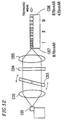
- Figure 12 is a view showing a short wavelength light source apparatus according to the present invention incorporating a semiconductor laser as a pump light source for exciting a polarization inversion type waveguide element having a polarization inversion period of a split structure, and a thin film optical element stabilizing the oscillation wavelength of the semiconductor laser.
- Figure 13 is a view showing a conventional short wavelength light source apparatus incorporating a semiconductor laser and a polarization inversion type waveguide element, in which grating feedback technique is used.
- Figure 14 is a graph showing the respective output power stabilities of a short wavelength light source apparatus according to the present invention incorporating a transmission type filter, and a conventional short wavelength light source apparatus in which grating feedback technique is used.
- Figure 15 is a view showing a semiconductor-laser-excited solid laser short wavelength light source apparatus according to the present invention incorporating a thin film optical element (reflective type filter) stabilizing the oscillation wavelength of the semiconductor laser.
- Figure 16 is a graph showing a reflection spectrum of a thin film optical element (reflective type filter) according to the present invention.
- Figure 17 is a view showing a semiconductor-laser-excited solid laser short wavelength light source apparatus according to the present invention incorporating a thin film optical element (reflective type filter) stabilizing the oscillation wavelength of the semiconductor laser.
- Figure 18 is a view showing a semiconductor-laser-excited intracavity type short wavelength light source apparatus according to the present invention incorporating a thin film optical element (reflective type filter) stabilizing the oscillation wavelength of the semiconductor laser.
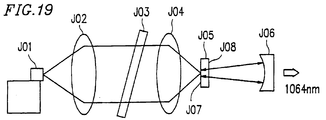
- Figure 19 is a view showing semiconductor-laser-excited solid laser short wavelength light source apparatus according to the present invention incorporating a thin film optical element (transmission type filter) stabilizing the oscillation wavelength of the semiconductor laser.
- a thin film optical element transmission type filter
- Figure 20 is a graph showing a transmission spectrum of a thin film optical element (transmission type filter) according to the present invention.
- Figure 21 is a view showing a semiconductor-laser-excited solid laser short wavelength light source apparatus according to the present invention incorporating a thin film optical element (transmission type filter) stabilizing the oscillation wavelength of the semiconductor laser.
- Figure 22 is a view showing a semiconductor-laser-excited intracavity type short wavelength light source apparatus according to the present invention incorporating a thin film optical element (transmission type filter) stabilizing the oscillation wavelength of the semiconductor laser.
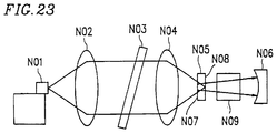
- Figure 23 is a view showing a semiconductor-laser-excited intracavity type short wavelength light source apparatus according to the present invention incorporating a thin film optical element (transmission type filter) stabilizing the oscillation wavelength of the semiconductor laser.
- Figure 24A is a view showing a short wavelength light source apparatus according to the present invention in which a dielectric multilayer film is provided on an outgoing end face of a semiconductor laser.
- Figure 24B is a view showing a short wavelength light source apparatus according to the present invention in which a dielectric multilayer film is provided on an incident end face of a laser medium.
- Figure 24C is a view showing a short wavelength light source apparatus according to the present invention in which a dielectric multilayer film is provided on an outgoing end face of a laser medium.
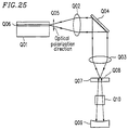
- Figure 25 is a view showing a conventional short wavelength light source apparatus incorporating a semiconductor laser and an intracavity type solid laser, in which grating feedback technique is used.
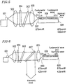
- FIG. 1 schematically shows a configuration for a short wavelength light source apparatus according to a first example of the present invention.
- the short wavelength light source apparatus includes a semiconductor laser 101 including an active layer (not shown) for emitting laser light, an optical wavelength converting element 106 for receiving at least a portion of the generated laser light so as to generate short wavelength light (harmonics) having a shorter wavelength than that of the laser light.
- the semiconductor laser 101 is a 150 mW-class single longitudinal mode laser with an oscillation wavelength of the 870 nm band.
- the optical wavelength converting element 106 is a polarization inversion type waveguide element.
- This short wavelength light source apparatus includes a thin film optical element 103 in addition to an ordinary optical system including lenses, etc.
- the thin film optical element 103 selectively reflects a portion of laser light generated by the semiconductor laser 101 that belongs to a predetermined wavelength band so as to feed back the reflected light to the active layer of the semiconductor laser 101 .
- the thin film optical element 103 may be, for example, a band-stop type (reflective type) filter formed of a dielectric multilayer film, and can be obtained by forming a layer of dielectric material such as SiO2 and TiO2 on a glass substrate having a thickness of 0.5 mm.
- Figure 2 shows reflection characteristics of the thin film optical element 103 .
- the reflectance of the thin film optical element 103 has a peak of about 10%.
- Light in the vicinity of the 870 nm band is optically fed back to the active layer of the semiconductor laser 101 by the thin film optical element 103 .
- the thin film optical element 103 feeds back a relatively wide spectrum width of about 5 nm of reflected light to the active layer of the semiconductor laser 101 .
- the short wavelength light source apparatus of the present example As is shown in Figure 1 , light generated by the semiconductor laser 101 is collimated by a lens 102 (N.A.: 0.55), and then is incident to the thin film optical element 103 .
- the thin film optical element 103 is disposed perpendicularly to the optical axis of the semiconductor laser 101 .
- a portion (about 10% or less) of light incident to the thin film optical element 103 that is in the vicinity of the 870 nm band is optically fed back to the active layer of the semiconductor laser 101 .
- the rest of the laser light i.e. a portion of the laser light which is not reflected by the thin film optical element 103 , is transmitted through the thin film optical element 103 .
- the thin film optical element 103 feeds back a relatively wide spectrum width of about 5 nm of reflected light to the active layer of the semiconductor laser 101 .
- the semiconductor laser 101 of the present example achieved a stable oscillation in a single longitudinal mode by feeding back the reflected light having the above-mentioned spectrum, and the oscillation wavelength was stabilized at 870 nm.
- the polarization direction of the laser light transmitted through the thin film optical element 103 is rotated by 90° around the optical axis by means of a ⁇ /2 plate 104 .
- the laser light after being transmitted through the ⁇ /2 plate 104 , is focused on an incident end face of the polarization inversion type waveguide element (optical wavelength converting element) 106 by a focusing lens 105 .
- the laser light having a wavelength of 870 nm is converted into blue light having a wavelength of 435 nm while being propagated through a waveguide 108 .
- blue light is stably emitted from an end face of the polarization inversion type waveguide element 106 (hereinafter, this end face of a given waveguide will be referred to as an 'outgoing end face').
- the polarization inversion type waveguide element 106 includes a LiTaO3 substrate 109 , an optical waveguide 108 (width: 4 ⁇ m) formed on the LiTaO3 substrate 109 , and polarization-inverted layers 107 (period: 4 ⁇ m).
- the polarization inversion type waveguide element 106 is formed in the following manner.
- a Ta film is deposited on the LiTaO3, and thereafter is patterned into a periodic pattern by using a usual photoprocess and a dry etching method, whereby a plurality of slits are formed in the Ta film.
- the LiTaO3 substrate is subjected to a proton exchanging process for 30 minutes at 260°C, so as to form a proton exchanged layer (thickness: 0.8 ⁇ m) under the slits in the Ta layer.
- the LiTaO3 substrate 109 is subjected to a heat treatment for 10 minutes at 590°C.
- the temperature during the heat treatment is increased at a rate (elevation rate) of 10°C/min., and is decreased at a rate (cooling rate) of 50°C/min.
- the Li concentration in regions directly below the proton exchanged layer of the LiTaO3 109 decreases, so that the Curie temperature in such regions decreases.
- the regions under the proton exchanged layer have the capability of locally conducting polarization inversion.
- the polarization-inverted layers 107 are formed in the LiTaO3 substrate 109 .
- the LiTaO3 substrate is subjected to an etching process for 2 minutes with the use of a solution of HF and HNF3 mixed at a ratio of 1:1 so as to remove the Ta film.
- the optical waveguide 108 is formed in the polarization-inverted layers 107 by a proton exchange process.
- Ta is patterned to a stripe shape so as to form a Ta mask for forming the optical waveguide 108 .
- the Ta mask thus obtained has slits each having a width of 4 ⁇ m and a length of 12 mm.
- the LiTaO3 substrate 109 which is covered with the above-mentioned Ta mask, is subjected to a proton exchange process for 16 minutes at 260°C so as to form high refractive index layer having a thickness of 0.5 ⁇ m, and is subjected to a heat treatment for 10 minutes at 380 °C after removing the Ta mask.
- the refractive index of the LiTaO3 substrate 109 is about 2.2, Fresnel reflection of about 14% is inevitably generated unless a coating is provided on end faces thereof. If Fresnel reflection is present, there emerges light returning to the semiconductor laser 101 , thereby hindering stabilization of the oscillation wavelength by the thin film optical element 103 . Therefore, it is preferable to form an AR coating which does not reflect light having a wavelength of 870 nm on the incident end face and the outgoing end face of the polarization inversion type waveguide element 106 .
- the ⁇ /2 plate 104 inserted in the optical system composed essentially of the collimating lens 102 and the focusing lens 105 may alternatively be formed on the thin film optical element 103 . In that case, the number of the component elements of the short wavelength light source apparatus would be reduced, thereby facilitating further miniaturization of the short wavelength light source apparatus.
- the polarization inversion type waveguide element 106 including a substrate composed of LiTaO3(LT) is used as an optical wavelength converting element in the short wavelength light source apparatus shown in Figure 1
- similarly stable short wavelength light can be obtained by using: a polarization inversion type waveguide element including a substrate composed of LiNbO3(LN) or KTiOPO4(KTP); a non-linear optical crystal having a large non-linear optical constant, e.g. KNbO3(KN); or a polarization inversion type bulk element including a substrate composed of LT, LN, or KTP.
- An AR coating which does not reflect light having a wavelength of 870 nm is provided on an incident end face and an outgoing end face of the optical wavelength converting element according to the present example.
- Deep polarization-inverted layers can be fabricated by a drawing method using an electron beam (EB), a focusing ion beam (FIB) method, etc., and by a proton exchange method.
- EB electron beam
- FIB focusing ion beam
- a polarization inversion type bulk element can be fabricated by any of the following four methods.
- a substrate composed of a dielectric material of LiNbO3 or LiTaO3 is irradiated with charged particles (electrons) accelerated at an acceleration voltage in the range of 10 to 100 keV in such a manner that the current density at a surface of the substrate becomes 1 to 1000 ⁇ A/mm2 while applying an electric field of 10 V/mm to 100kV/mm.
- charged particles electrospray particles
- a metal film is vapor deposited on a +C plane of a substrate composed of a dielectric material of LiNbO3 or LiTaO3 (C plates), and is grounded.
- An electron beam accelerated at an acceleration voltage of 25 keV is focused so as to be radiated on each substrate from a -C plane thereof so that the polarization at the irradiated portion is inverted.
- the polarization-inverted layers thus obtained reach the bottom face of the substrate (thickness: 0.5 mm). Thus, deep polarization-inverted layers can be obtained.
- Si2+ ions are focused and radiated on a substrate, the Si2+ ions having been separated and selected by means of an electric field filter.
- the focused area extends about 1 ⁇ m ⁇ .
- the substrate is a C plate composed of LiTaO3, which is grounded to a sample holder with metal paste.
- the Si2+ ions are focused on the +C plane of the substrate. A periodic scanning is conducted with the focused ions while utilizing computer control.
- the above-mentioned irradiation is conducted under the conditions that: the acceleration energy is 200 keV; the amount of current is 120 pA; and the scanning velocity is 84 ⁇ m/sec.
- the polarization-inverted layers thus obtained reach the bottom face of the substrate, and has a width of 1.8 ⁇ m.
- the width of each polarization-inverted layer is uniform along the depth direction of the polarization-inverted layer.
- periodic polarization-inverted layers (period:4 ⁇ m) under the same conditions as above, a uniform periodic structure having a period of 4 ⁇ m was formed, with the width and the depth of each polarization-inverted layer being 1.8 ⁇ m and 0.5 mm, respectively.
- Ta is vapor deposited on a -C plane of a LiTaO3 substrate and is subjected to a photolithography and a dry etching so as to form stripes having a period of 4 ⁇ m.
- Several drops of pyrophoric acid are placed on the stripes, and a heat treatment is conducted for 30 minutes on a hot plate heated at 230°C.
- a heat treatment is conducted for 30 minutes on a hot plate heated at 230°C.
- the short wavelength light source apparatus shown in Figure 3 includes a semiconductor laser 301 including an active layer (not shown) for emitting laser light, an optical wavelength converting element 306 for receiving at least a portion of the generated laser light so as to generate short wavelength light (harmonics) having a shorter wavelength than that of the laser light.
- the semiconductor laser 301 is a 150 mW-class single longitudinal mode laser with an oscillation wavelength of the 870 nm band.
- the optical wavelength converting element 306 is a polarization inversion type waveguide element.
- This short wavelength light source apparatus includes a thin film optical element 303 in addition to an ordinary optical system including lenses, etc.
- the thin film optical element 303 selectively transmits a portion of laser light generated by the semiconductor laser 301 that belongs to a predetermined wavelength band. A portion of the transmitted light is fed back to the active layer of the semiconductor laser 301 , as is described later in the present specification.
- the thin film optical element 303 may be, for example, a band-pass type (transmission type) filter formed of a dielectric multilayer film, and can be obtained by forming a few dozens of layers of dielectric material such as TiO2 on a glass substrate having a thickness of 0.5 mm.
- Figure 4 shows transmission characteristics of the thin film optical element 303 .
- the reflectance of the thin film element 303 has a maximum transmittance of about 80% at a wavelength of 870 nm.
- the half-width of the transmission spectrum of the thin film element 303 is 1 nm.
- the transmittance of the thin film optical element 303 has angle dependence.
- the transmission spectrum shown in Figure 4 represents a spectrum in the case where the principal plane of the thin film optical element 303 is disposed at an angle (i.e. incident angle) of 20° with the optical axis.
- the shift amount of the transmission center wavelength of the thin film optical element 303 has an angle dependence of 1.5 nm/deg; when the incident angle is in the vicinity of 10°, the shift amount of the transmission center wavelength has an angle dependence of 0.9 nm/deg; and when the incident angle is 0°, the shift amount of the transmission center wavelength has substantially no angle dependence.
- the short wavelength light source apparatus of the present example As is shown in Figure 3 , light generated by the semiconductor laser 301 is collimated by a lens 302 , and then is incident to the thin film optical element 303 .
- the thin film optical element 303 is disposed obliquely with respect to the optical axis of the semiconductor laser 301 .
- only light having a wavelength in the vicinity of 870 nm is selectively transmitted through the thin film optical element 303 when the thin film optical element 303 is disposed at an angle of 20° with the optical axis of the semiconductor laser 301 .
- the rest of the laser light i.e.
- the thin film optical element 303 a portion of the laser light which is not transmitted through the thin film optical element 303 , is reflected by the thin film optical element 303 .
- the reflected light is not fed back to the active layer of the semiconductor laser 301 , since the thin film optical element 303 is disposed obliquely with respect to the optical axis of the semiconductor laser 301 .
- the polarization direction of the laser light transmitted through the thin film optical element 303 is rotated by 90° around the optical axis by means of a ⁇ /2 plate 304 .
- the laser light, after being transmitted through the ⁇ /2 plate 304 is focused on an incident end face 307 of the polarization inversion type waveguide element (optical wavelength converting element) 306 by a focusing lens 305 .
- An AR coating is provided on the incident end face 307 of the polarization inversion type waveguide element 306 ; otherwise, Fresnel reflection of about 14% would inevitably be generated.
- the semiconductor laser 301 achieves stable oscillation in a single longitudinal mode, with the oscillation wavelength being stabilized at 870 nm.
- the light (wavelength: 870 nm) emitted from the incident end face 307 of the polarization inversion type waveguide element 306 and coupled to a waveguide of the polarization inversion type waveguide element 306 is converted into blue light having a wavelength of 435 nm while being propagated through the waveguide.
- blue light is stably emitted from an outgoing end face 308 of the polarization inversion type waveguide element 306 .
- a portion of the light coupled to the above-mentioned waveguide is Fresnel reflected by the outgoing end face 308 . Since it is preferable to restrain light having a wavelength of 870 nm from being reflected by the outgoing end face 308 , an AR coating which does not reflect the fundamental wave (wavelength: 870 nm) is provided on the outgoing end face 308 .
- the polarization inversion type waveguide element 306 includes polarization-inverted layers having a period of 4 ⁇ m and an optical waveguide having a width of 4 ⁇ m and formed in an LiTaO3 substrate, as in the case of the polarization inversion type waveguide element 106 in Example 1.
- the fundamental wave (870 nm) is converted into light having a wavelength of 435 nm.
- blue light is obtained through the outgoing end face 308 of the polarization inversion type waveguide element 306 .
- the polarization inversion type waveguide element 306 has a length of 10 mm and a conversion efficiency of 200%/W. As a result, a harmonic wave of about 10 mW is obtained, the fundamental wave power of about 70 mW being coupled to the waveguide. It is preferable to provide an AR coating which does not reflect the 430 nm harmonic wave on the outgoing end face 308 so that the harmonic light can be obtained at even higher efficiency.
- Figure 14 shows temporal change in the output power of the short wavelength light source apparatus of the present example in comparison with a case where a grating is employed.
- the polarization inversion type waveguide element 306 is stable as a function of time as well, since the wavelength shifts by a smaller amount depending on the angle when using a filter than when using a grating.
- the wavelength does not shift depending on the angle by such a large amount as 28 nm/deg as in the case where a grating is used. Therefore, the adjustment using the thin film optical element 303 is facilitated, and the short wavelength light source apparatus is made stable against temporal deterioration even if configurated as a module.
- the short wavelength light source apparatus of the present example is stable against temperature changes as well (wavelength shift against temperature changes: 0.005 nm/°C).
- the short wavelength light source apparatus is also stable against changes in moisture.
- an AR coating which does not reflect laser light generated from a semiconductor laser is provided on an end face of a polarization inversion type waveguide element.
- the longitudinal mode of the semiconductor laser may become unstable due to a small amount of light reflected by the end face, which amount of light is fed back to the semiconductor laser.
- the present example effectively utilizes the returned light due to the reflection so as to stabilize the oscillation of the semiconductor laser. Therefore, the present example has considerable practical significance.
- Fresnel reflection at the incident end face of the polarization inversion type waveguide element is utilized in the present example, it is also applicable to optimize the reflection amount by providing an appropriate reflection coating on the incident end face so as to adjust the reflection amount at the incident end face.
- a reflection coating having a reflectance of about 5% on the other hand, the output power of the harmonic light increases due to an increase in the amount of light coupled to the waveguide.
- the ⁇ /2 plate 304 disposed in the optical system may alternatively be formed on the thin film optical element 303 . In that case, the number of the component elements of the short wavelength light source apparatus would be reduced, thereby facilitating further miniaturization of the short wavelength light source apparatus.
- the peak wavelength of the transmission spectrum of the thin film optical element 303 has angle dependence.
- a rotation mechanism By mounting a rotation mechanism on the thin film optical element 303 and adjusting the angle of the thin film optical element 303 with respect to the laser light by means of the rotation mechanism, it becomes possible to control the peak wavelength of the transmission spectrum at a high accuracy.
- the rotation mechanism By using such a rotation mechanism, it becomes possible to monitor the output power of harmonic wave obtained from the outgoing end face 308 of the polarization inversion type waveguide element 306 .
- the angle which the thin film optical element 303 constitutes with the laser light is adjusted by monitoring the output power of harmonic wave obtained from the outgoing end face 308 of the polarization inversion type waveguide element 306 so that the monitored output power is maximized.
- the oscillation wavelength of the semiconductor laser 301 can be made equal to the phase matching wavelength of the polarization inversion type waveguide element 306 .
- the oscillation wavelength of the semiconductor laser 301 can be stabilized against changes in the refractive index of the substrate of the polarization inversion type waveguide element 306 due to changes in the temperature of the thin film optical element 303 and/or optical damage (photorefractive effect), so that stable output power of the harmonic wave can be obtained.
- a rotation monitor and/or an actuator may be used as the rotation mechanism. It is also applicable to use a piezo element on a fulcrum so that the piezo element has a rotatory action.
- thin film optical element 303 is disposed between the semiconductor laser 301 and the polarization inversion type waveguide element 306 in the present example, a plurality of thin film optical elements may alternatively be inserted therein, so that the half width of the transmission spectrum shown in Figure 4 becomes substantially narrow, thereby improving the wavelength selectivity.
- the polarization inversion type waveguide element 306 including a substrate composed of LiTaO3(LT) is used as an optical wavelength converting element in the short wavelength light source apparatus shown in Figure 3
- similarly stable short wavelength light can be obtained by using: a polarization inversion type waveguide element including a substrate composed of LiNbO3(LN) or KTiOPO4(KTP); an organic or inorganic non-linear optical crystal (a ring resonator structure, phase matching type waveguide device, etc.) having a large non-linear optical constant, e.g. KNbO3(KN); or a polarization inversion type bulk element including a substrate composed of LT, LN, or KTP described in Example 2.
- an AR coating which reflects neither light having a wavelength of 870 nm nor light having a wavelength of 435 nm on an incident end face and an outgoing end face of the optical wavelength converting element.
- the short wavelength light source apparatus shown in Figure 5 includes a semiconductor laser 501 including an active layer (not shown) for emitting laser light, an optical wavelength converting element 506 for receiving at least a portion of the generated laser light so as to generate short wavelength light (harmonics) having a shorter wavelength than that of the laser light.
- the semiconductor laser 501 is a 150 mW-class single longitudinal mode laser with an oscillation wavelength of the 870 nm band.
- the optical wavelength converting element 506 is a polarization inversion type waveguide element.
- This short wavelength light source apparatus includes a thin film optical element 503 having the same structure as that of the thin film optical element 303 in Example 3. Accordingly, the thin film optical element 503 has the transmission characteristics shown in Figure 4.
- the present example is characterized in that Fresnel reflection occurring at an outgoing end face 508 of the polarization inversion type waveguide element 506 is utilized as returned light to the semiconductor laser 501 .
- An incident end face of the polarization inversion type waveguide element 506 has a low reflectance. It is preferable to provide an AR coating on the incident end face 507 .
- Light emitted from the semiconductor laser 501 is focused on the incident end face of the polarization inversion type waveguide element 506 so as to be coupled to an optical waveguide of the polarization inversion type waveguide element 506 .
- An outgoing end face of the semiconductor laser 501 and the incident end face 507 of the polarization inversion type waveguide element 506 are confocally disposed.
- the outgoing end face of the semiconductor laser 501 also constitutes a confocal system with the outgoing end face 508 of the polarization inversion type waveguide element 506 .
- light reflected by the outgoing end face 508 is all optically fed back to the active layer of the semiconductor laser 501 .
- the thin film optical element 503 is not provided, the above-mentioned reflected light (returned light) may cause the semiconductor laser 501 to have mode hopping or to have a multitude of modes.
- the thin film optical element 503 between the semiconductor laser 501 and the polarization inversion type waveguide element 506 is provided at an angle of 20° with the optical axis, so that only light having a wavelength in the vicinity of 870 nm is incident to the incident end face 507 and coupled to the optical waveguide, so that only light having a wavelength in the vicinity of 870 nm which is reflected by the outgoing end face 508 of the polarization inversion type waveguide element 506 is optically fed back to the semiconductor laser 501 .
- the longitudinal mode of the semiconductor laser 501 is stabilized as a single mode in the vicinity of 870 nm.
- the amount of light returning to the semiconductor laser 501 can be increased, so as to further stabilize the operation of the short wavelength light source apparatus.
- HR high reflectance
- the thin film optical element 503 is disposed at an angle with the optical axis of the semiconductor laser 501 .
- the thin film optical element 503 reflects light having wavelengths other than those in the vicinity of 870 nm. In other words, light having wavelengths other than those in the vicinity of 870 nm is not optically fed back to the active layer of the semiconductor laser 501 .
- the fundamental wave (870 nm) coupled to the polarization inversion type waveguide element 506 is converted into light having a wavelength of 435 nm.
- the temperature-based tuning may be realized by, although not shown in Figure 5, fixing the polarization inversion type waveguide element 506 on a Peltier element, or providing a heater on the optical waveguide.
- the polarization inversion type waveguide element 506 has a length of 10 mm and a conversion efficiency of 200%/W. As a result, a harmonic wave of about 10 mW is obtained, the fundamental wave power of about 70 mW being coupled to the waveguide. It is preferable to provide an AR coating which does not reflect the 435 nm harmonic wave on the outgoing end face 508 of the polarization inversion type waveguide element 506 so that the harmonic light can be obtained at even higher efficiency.
- the harmonic wave obtained by converting the light fed back from the outgoing end face 508 to the semiconductor laser 501 is also reflected by the incident end face 507 so as to be obtained through the outgoing end face 508 , thereby achieving an even higher efficiency.
- a waveguide-type external resonator By further providing a coating having a reflectance of 97% and a coating having a reflectance of 99.9% on the incident end face 507 and the outgoing end face 508 , respectively, a waveguide-type external resonator can be constructed, which would increase the conversion efficiency to be twenty times as large.
- an AR coating which does not reflect laser light generated from a semiconductor laser is provided on an end face of a polarization inversion type waveguide element.
- the longitudinal mode of the semiconductor laser may become unstable due to a small amount of light reflected by the end face, which amount of light is fed back to the semiconductor laser.
- the present example effectively utilizes the returned light due to the reflection so as to stabilize the longitudinal mode of the semiconductor laser. Therefore, the present example has considerable practical significance.
- the ⁇ /2 plate 504 disposed in the optical system may alternatively be formed on the thin film optical element 503 .
- the number of the component elements of the short wavelength light source apparatus would be reduced, thereby facilitating further miniaturization of the short wavelength light source apparatus.
- the harmonic output power can be stabilized.
- the polarization inversion type waveguide element 506 including a substrate composed of LiTaO3(LT) is used as an optical wavelength converting element in the short wavelength light source apparatus shown in Figure 5
- similarly stable short wavelength light can be obtained by using a polarization inversion type waveguide element including a substrate composed of LiNbO3(LN) or KTiOPO4(KTP), a phase matching type waveguide device composed of KN, etc., or the like.
- the short wavelength light source apparatus of the present example incorporates a thin film optical element 603 (band-pass type filter) having a transmission spectrum shown in Figure 4 .
- a polarization inversion type waveguide element 606 is used as an optical wavelength converting element.
- the semiconductor laser 601 is a 150 mW-class single longitudinal mode laser with an oscillation wavelength of the 870 nm band.
- Reference numeral 602 denotes a collimating lens (N.A.: 0.55);
- 604 denotes a ⁇ /2 plate;
- 605 denotes a focusing lens for coupling light to the waveguide.
- a wavelength selection mirror 607 is an optical element for separating a harmonic wave obtained by wavelength conversion from the fundamental light.
- the polarization inversion type waveguide element 606 includes polarization-inverted layers (period: 4 ⁇ m) formed in a LiTaO3 substrate, and an optical waveguide (width: 4 ⁇ m) as in Example 1.
- an HR coating for reflecting the fundamental wave (wavelength: 870 nm) and a harmonic wave (wavelength: 435 nm) is provided on an end face 609 of the polarization inversion type waveguide element 606 .
- An AR coating which reflects neither light having a wavelength of 870 nm nor light having a wavelength of 435 nm is provided on an incident end face 608 of the polarization inversion type waveguide element 606 so as to reduce the reflectance of the incident end face 608 .
- Laser light emitted from the semiconductor laser 601 is transmitted through the thin film optical element 603 , and then focused on the incident end face 608 of the polarization inversion type waveguide element 606 by the focusing lens 605 so as to be coupled to the waveguide.
- An outgoing end face of the semiconductor laser 601 and the incident end face 608 of the polarization inversion type waveguide element 606 are confocally disposed.
- the outgoing end face of the semiconductor laser 601 also constitutes a confocal system with the end face 609 of the polarization inversion type waveguide element 606 .
- light reflected by the end face 609 is all optically fed back to an active layer of the semiconductor laser 601 . If the thin film optical element 603 is not provided, the above-mentioned reflected light (returned light) may cause the semiconductor laser 601 to have mode hopping or to have a multitude of modes.
- the thin film optical element 603 By disposing the thin film optical element 603 between the semiconductor laser 601 and the polarization inversion type waveguide element 606 at an angle of 20° with the optical axis, it is ensured that only light having a wavelength in the vicinity of 870 nm is incident to the incident end face 608 and coupled to the optical waveguide, so that only light having a wavelength in the vicinity of 870 nm which is reflected by the end face 609 is transmitted back through the thin film element 603 so as to be optically fed back to the semiconductor laser 601 . As a result, the longitudinal mode of the semiconductor laser 601 is stabilized as a single mode in the vicinity of 870 nm.
- an HR coating for reflecting light having a wavelength of 870 nm and light having a wavelength of 435 nm (preferably at a 100% reflectance) is provided on the end face 609 .
- the fundamental wave and the harmonic wave interact with each other also when being propagated backwards, i.e. from the end face 609 to the semiconductor laser 601 . Therefore, the inter-action length obtained by the polarization inversion type waveguide element 606 becomes twice as large, so that the conversion efficiency into the harmonic wave becomes four times as large.
- the fundamental wave (870 nm) coupled to the polarization inversion type waveguide element 606 is converted into a harmonic wave having a wavelength of 435 nm.
- blue light goes out through the incident end face 608 of the polarization inversion type waveguide element 606 .
- the blue light is separated from the fundamental wave by the wavelength selection mirror 607 .
- the polarization inversion type waveguide element 606 has a length of 10 mm and a conversion efficiency of 800%/W. As a result, a harmonic wave of about 30 mW is obtained, the fundamental wave power of about 70 mW being coupled to the waveguide.
- the reflectance of the end face 609 is made large.
- the harmonic light is obtained with higher stability but also the interaction length of the optical wavelength converting element (polarization inversion type waveguide element) 606 is increased. Therefore, the present example has considerable practical significance.
- the ⁇ /2 plate 604 disposed in the optical system may alternatively be formed on the thin film optical element 603 .
- the number of the component elements of the short wavelength light source apparatus may be reduced, thereby facilitating further miniaturization of the short wavelength light source apparatus.
- the number of the component elements of the short wavelength light source apparatus may be further reduced and further miniaturization of the short wavelength light source apparatus would be facilitated by forming the wavelength selection mirror 607 disposed in the optical system on the thin film optical element 603 .
- the harmonic output power can be stabilized by providing a rotation mechanism and a feedback circuit for the thin film optical element 603 .
- the polarization inversion type waveguide element 606 including a substrate composed of LiTaO3(LT) is used as an optical wavelength converting element in the short wavelength light source apparatus shown in Figure 6
- similarly stable short wavelength light can be obtained by using a polarization inversion type waveguide element including a substrate composed of LiNbO3(LN) or KTiOPO4(KTP), a phase matching type waveguide device composed of KN, etc., or the like.
- an AR coating which reflects neither light having a wavelength of 870 nm nor light having a wavelength of 435 nm on an incident face of the optical wavelength converting element and to provide an HR coating for reflecting light having a wavelength of 870 nm and light having a wavelength of 435 nm on an outgoing face of the optical wavelength converting element.
- the short wavelength light source apparatus of the present example incorporates a thin film optical element 703 (band-pass type filter) having a transmission spectrum shown in Figure 4 .
- a polarization inversion type bulk element 705 is used as an optical wavelength converting element.
- the semiconductor laser 701 is a 150 mW-class single longitudinal mode laser with an oscillation wavelength of the 870 nm band.
- Reference numeral 702 denotes a collimating lens (N.A.: 0.55); and 704 denotes a long-focus focusing lens (N.A.: 0.2) for focusing light on the polarization inversion type bulk element 705 .
- the polarization inversion type waveguide element 705 includes deep polarization-inverted layers (period: 4 ⁇ m) formed in a LiTaO3 substrate by a similar manner to that used in Example 2.
- the reflectance of an incident end face 706 of the polarization inversion type bulk element 705 is reduced, preferably by providing an AR coating on the incident end face 706 , so as to utilize light reflected by an outgoing end face 707 as light returning to the semiconductor laser 701 .
- Light emitted from the semiconductor laser 701 is focused on the outgoing end face 707 of the polarization inversion type bulk element 705 .
- An outgoing end face of the semiconductor laser 701 and the incident end face 706 of the polarization inversion type bulk element 705 are confocally disposed. As a result, light reflected by the outgoing end face 707 is all optically fed back to an active layer of the semiconductor laser 701 . If the thin film optical element 703 is not provided, the above-mentioned reflected light (returned light) may cause the semiconductor laser 701 to have mode hopping or to have a multitude of modes.
- the thin film optical element 703 By disposing the thin film optical element 703 between the semiconductor laser 701 and the polarization inversion type bulk element 705 at an angle of 20° with the optical axis, it is ensured that only light having a wavelength in the vicinity of 870 nm is incident to the polarization inversion type bulk element 705 , so that only light having a wavelength in the vicinity of 870 nm which is reflected by the outgoing end face 707 is transmitted back through the thin film element 703 so as to be optically fed back to the semiconductor laser 701 . As a result, the longitudinal mode of the semiconductor laser 701 is stabilized as a single mode in the vicinity of 870 nm.
- the amount of light returning to the semiconductor laser 701 can be increased, so as to further stabilize the operation of the short wavelength light source apparatus.
- the thin film optical element 703 is disposed obliquely with respect to the optical axis of the semiconductor laser 701 .
- the thin film optical element 703 reflects light having wavelengths other than those in the vicinity of 870 nm. In other words, light having wavelengths other than those in the vicinity of 870 nm is not optically fed back to the active layer of the semiconductor laser 701 .
- the fundamental wave (870 nm) coupled to the polarization inversion type bulk element 705 is converted into a harmonic wave having a wavelength of 435 nm.
- the polarization inversion type bulk element 705 has a length of 2 mm and a conversion efficiency of 8%/W.
- a harmonic wave of about 0.4 mW is obtained, the fundamental wave power of about 70 mW being coupled to the waveguide.
- an AR coating which does not reflect laser light generated from a semiconductor laser is provided on an end face of a polarization inversion type bulk element.
- the longitudinal mode of the semiconductor laser may become unstable due to a small amount of light reflected by the end face, which amount of light is fed back to the semiconductor laser.
- the present example effectively utilizes the returned light due to the reflection so as to stabilize the longitudinal mode of the semiconductor laser. Therefore, the present example has considerable practical significance.
- An even higher harmonic output power can be obtained by using a 1 W-class single longitudinal mode laser including a light amplifying portion as the pump laser source.
- the harmonic output power can be stabilized by providing a rotation mechanism and a feedback circuit for the thin film optical element 703 , as in Example 3.
- the polarization inversion type waveguide element 705 including a substrate composed of LiTaO3(LT) is used as an optical wavelength converting element in the short wavelength light source apparatus shown in Figure 7
- similarly stable short wavelength light can be obtained by using: a polarization inversion type bulk element including a substrate composed of LiNbO3(LN) or KTiOPO4(KTP); or an organic or inorganic non-linear optical crystal (a ring resonator structure, phase matching type waveguide device, etc.) having a large non-linear optical constant, e.g. KNbO3(KN).
- an AR coating which does not reflect light having a wavelength of 870 nm on an incident end face of the optical wavelength converting element, and to provide an HR coating for reflecting light having a wavelength of 870 nm and an AR coating which does not reflect light having a wavelength of 435 nm on an outgoing end face of the optical wavelength converting element.
- the short wavelength light source apparatus of the present example incorporates a thin film optical element 803 (band-pass type filter) having a transmission spectrum shown in Figure 4 .
- a polarization inversion type bulk element 805 is used as an optical wavelength converting element.
- the semiconductor laser 801 is a 150 mW-class single longitudinal mode laser with an oscillation wavelength of the 870 nm band.
- Reference numeral 802 denotes a collimating lens (N.A.: 0.55); and 804 denotes a long-focus focusing lens (N.A.: 0.2) for focusing light on the polarization inversion type bulk element 805 .
- a wavelength selection mirror 806 is an optical element for separating a harmonic wave obtained by wavelength conversion from the fundamental light.
- the polarization inversion type waveguide element 805 includes deep polarization-inverted layers (period: 4 ⁇ m) formed in a LiTaO3 substrate by a similar manner to that used in Example 2.
- An HR coating for reflecting light having a wavelength of 870 nm and light having a wavelength of 435 nm is provided on an end face 808 of the polarization inversion type bulk element 805 .
- the reflectance of an incident end face 807 of the polarization inversion type bulk element 805 is reduced by providing an AR coating which reflects neither light having a wavelength of 870 nm nor light having a wavelength of 435 nm thereon.
- Light emitted from the semiconductor laser 801 is led through the thin film optical element 803 so as to be focused by the focusing lens 804 on the end face 808 of the polarization inversion type bulk element 805 .
- An outgoing end face of the semiconductor laser 801 and the end face 808 of the polarization inversion type bulk element 805 are confocally disposed.
- light reflected by the end face 808 is optically fed back to an active layer of the semiconductor laser 801 .
- the thin film optical element 803 is not provided, the above-mentioned reflected light (returned light) may cause the semiconductor laser 801 to have mode hopping or to have a multitude of modes.
- the thin film optical element 803 By disposing the thin film optical element 803 between the semiconductor laser 801 and the polarization inversion type bulk element 805 at an angle of 20° with the optical axis, it is ensured that only light having a wavelength in the vicinity of 870 nm is incident to the polarization inversion type bulk element 805 , so that only light having a wavelength in the vicinity of 870 nm which is reflected by the end face 808 is transmitted back through the thin film element 803 so as to be optically fed back to the semiconductor laser 801 . As a result, the longitudinal mode of the semiconductor laser 801 is stabilized as a single mode in the vicinity of 870 nm.
- an HR coating for reflecting light having a wavelength of 870 nm and light having a wavelength of 435 nm (preferably at a 100% reflectance) is provided on the end face 808 .
- the fundamental wave and the harmonic wave interact with each other also when being propagated backwards, i.e. from the end face 808 to the semiconductor laser 801 . Therefore, the interaction length obtained by the polarization inversion type bulk element 805 becomes twice as large, so that the conversion efficiency into the harmonic wave becomes four times as large.
- the fundamental wave (870 nm) coupled to the polarization inversion type bulk element 805 is converted into a harmonic wave having a wavelength of 435 nm.
- blue light goes out through the incident end face 807 of the polarization inversion type bulk element 805 .
- the blue light is separated from the fundamental wave by the wavelength selection mirror 806 .
- the polarization inversion type bulk element 805 has a length of 2 mm and a conversion efficiency of 32%/W. As a result, a harmonic wave of about 1.6 mW is obtained.
- the reflectance of the end face 808 is made large. As a result, not only that the harmonic light is obtained with higher stability but also the interaction length of the optical wavelength converting element (polarization inversion type waveguide element) 805 is increased. Therefore, the present example has a considerable practical significance.
- the wavelength selection mirror 806 inserted in the optical system composed essentially of the collimating lens 802 and the focusing lens 804 may alternatively be formed on the thin film optical element 803 . In that case, the number of the component elements of the short wavelength light source apparatus would be reduced, thereby facilitating further miniaturization of the short wavelength light source apparatus.
- An even higher harmonic output power can be obtained by using a 1 W-class single longitudinal mode laser including a light amplifying portion as the pump laser source.
- the harmonic output power can be stabilized by providing a rotation mechanism and a feedback circuit for the thin film optical element 803 , as in Example 3.
- the polarization inversion type bulk element 805 including a substrate composed of LiTaO3(LT) is used as an optical wavelength converting element in the short wavelength light source apparatus shown in Figure 8
- similarly stable short wavelength light can be obtained by using: a polarization inversion type bulk element including a substrate composed of LiNbO3(LN) or KTiOPO4(KTP); or an organic or inorganic non-linear optical crystal (a ring resonator structure, phase matching type waveguide device, etc.) having a large non-linear optical constant, e.g. KNbO3(KN).
- an AR coating which reflects neither light having a wavelength of 870 nm nor light having a wavelength of 435 nm on an incident end face of the optical wavelength converting element, and to provide an HR coating for reflecting light having a wavelength of 870 nm and light having a wavelength of 435 nm on an outgoing end face of the optical wavelength converting element.
- a transmission type filter composed essentially of a dielectric multilayer film 903 on an outgoing end of the semiconductor laser 901 , as is shown in Figure 9A . It is also applicable to provide a transmission type filter or reflective type filter composed essentially of a dielectric multilayer film 904 on an incident end face of a polarization inversion type waveguide element 902 . In this case, too, the oscillation wavelength of the semiconductor laser 901 can be stabilized. Thus, stable wavelength conversion and harmonic light can be provided.
- Light emitted from the semiconductor laser A01 has an emission angle of about 2° with respect to an outgoing end face of the semiconductor laser A01 .
- the outgoing end face of the semiconductor laser A01 is disposed at a distance of about 10 ⁇ m from an incident end face of a polarization inversion type waveguide element A02 (polarization inversion type waveguide element A02 in Figure 9B ).
- the normal axis of the incident end face of the polarization inversion type waveguide element A02 is disposed at an angle of 8° with the optical axis of the semiconductor laser A01 .
- a transmission type filter A03 has a transmittance of 80% for light having a wavelength of 870 nm which is incident thereto at an incident angle of 8°.
- the transmission spectrum of the transmission type filter A03 has a width of 1 nm. Although light having a wavelength in the vicinity of 870 nm is reflected by the transmission type filter A03 , the reflected light is not fed back to an active layer of the semiconductor laser A01 , since the normal axis of the transmission type filter A03 is disposed at an angle of 8° with the optical axis of the semiconductor laser A01 . On the other hand, an optical waveguide A04 formed in the polarization inversion type waveguide element A02 is disposed at angle of 3.6° with the normal axis of the incident end face of the polarization inversion type waveguide element A02 .
- An HR coating for reflecting light having a wavelength of 870 nm and an AR coating which does not reflect light having a wavelength of 435 nm is provided on the outgoing end face of the polarization inversion type waveguide element A02 .
- the light coupled to the waveguide A04 is converted into light having a wavelength of 435 nm, which goes out through the outgoing end face of the polarization inversion type waveguide element A02 .
- the polarization inversion type waveguide element A02 shown in Figure 10A is formed of an x-plate LiTaO3, since such a polarization inversion type waveguide element is more preferable because of the large coupling coefficient thereof with the semiconductor laser A01 .
- the coupling efficiency between the semiconductor laser A01 and the polarization inversion type waveguide element A02 can be still more increased by further providing a ⁇ /2 plate, which is commonly used for improving the coupling efficiency between a z-plate polarization inversion type waveguide element and a semiconductor laser, on the incident end face of the LiTaO3 substrate.
- the entire device incorporating the light source can be miniaturized, and temperature control is also facilitated, thereby making the device more practical.
- the polarization inversion type waveguide element A02 is used as an optical wavelength converting element.
- similarly stable short wavelength light can be obtained by using a polarization inversion type bulk element including a substrate composed of LiTaO3(LT), LiNbO3(LN) or KTiOPO4(KTP) or a non-linear optical crystal (a ring resonator structure, phase matching type waveguide device, etc.) having a large non-linear optical constant, e.g. KNbO3(KN), as an optical wavelength converting element, and by providing a thin film optical element on the incident end face or the outgoing end face of the optical wavelength converting element.
- a short wavelength light source apparatus incorporating a polarization inversion type bulk element A06 will be described with reference to Figure 10B .
- FIG. 10B As is shown in Figure 10B , light emitted from a semiconductor laser A05 is incident to an incident end face of the polarization inversion type bulk element A06 formed in a LiTaO3 substrate.
- a transmission type filter A07 provided on the incident end face of the polarization inversion type bulk element A06 transmits only light having a wavelength in the vicinity of 870 nm, which light is led to an outgoing end face of the polarization inversion type bulk element A06 .
- the outgoing end face of the polarization inversion type bulk element A06 is processed to a spherical shape, and has a curvature of 10 mm.
- An HR coating for reflecting light having a wavelength of 870 nm and an AR coating which does not reflect light having a wavelength of 435 nm are provided on the outgoing end face of the polarization inversion type bulk element A06 .
- Light reflected by the outgoing end face of the polarization inversion type waveguide element A06 is transmitted back through the transmission type filter A07 , and is focused on an outgoing end face of the semiconductor laser A05 so as to be optically fed back to an active layer thereof.
- the oscillation wavelength of the semiconductor laser short wavelength light source apparatus is stabilized in the vicinity of 870 nm.
- the oscillation wavelength of a semiconductor laser can be varied by varying an angle ⁇ at which a thin film optical element is disposed.
- a polarization inversion type bulk element or waveguide element of the short wavelength light source apparatus as to have a polarization inversion period of a chirp structure or a split structure, light having short wavelengths corresponding to the varying oscillation wavelengths of the semiconductor laser can be obtained.
- the wavelength of the short wavelength light can be tuned by varying the incident angle of laser light at which the laser light enters the thin film optical element.
- Figure 11A shows the polarization inversion type waveguide element 106 shown in Figure 1 .
- the first order polarization-inverted layers 107 having a period of 4.0 ⁇ m are uniformly formed in the LiTaO3 substrate 109 so that quasi-phase matching is achieved for light having a wavelength of 870 nm.
- Figure 11B shows a polarization inversion type waveguide element having a split structure.
- the polarization inversion type waveguide element shown in Figure 11B is 15 mm long.
- the polarization inversion type waveguide element is divided into three regions I , II , and III . Each region is 5 mm long.
- the polarization-inverted layers in region I have a period of 3.6 ⁇ m; the polarization-inverted layers in region II have a period of 3.8 ⁇ m; and the polarization-inverted layers in region III have a period of 4.0 ⁇ m.
- Quasi-phase matching is achieved for light having wavelengths of 850 nm, 860 nm, and 870 nm in regions I , II , and III , respectively.
- Regions I , II , and III output harmonics having wavelengths of, respectively, 425 nm, 430 nm, and 435 nm.
- Figure 12 shows a short wavelength light source apparatus incorporating a polarization inversion type waveguide element C06 which is identical with the polarization inversion type waveguide element shown in Figure 11B .
- Reference numeral C01 denotes a 150 mW-class single longitudinal mode semiconductor laser
- C02 denotes a collimating lens (N.A.: 0.55)
- C03 denotes a thin film optical element
- C04 denotes a ⁇ /2 plate
- C05 denotes a focusing lens for coupling light to a waveguide formed in the polarization inversion type waveguide element.
- the thin film optical element C03 is a band-pass filter composed essentially of a dielectric multilayer film having a transmittance of about 85%, and has a transmission spectrum with peak wavelengths of 870 nm, 860 nm, and 850 nm at incident angles of 1°, 15°, and 20°, respectively.
- the wavelength of the output harmonic wave can be varied by adjusting the angle ⁇ at which the thin film optical element C03 shown in Figure 12 is disposed.
- the polarization inversion type waveguide element C06 includes an optical waveguide (width: 4 ⁇ m) and the polarization-inverted layers shown in Figure 11B formed in a LiTaO3 substrate.
- An HR coating for reflecting light having a wavelength in the range of 850 nm to 870 nm is provided on an outgoing end face C08 of the polarization inversion type waveguide element C06 .
- An AR coating which does not reflect light having a wavelength in the range of 850 nm to 870 nm is provided on an incident end face C07 of the polarization inversion type waveguide element C06 .
- Light emitted from the semiconductor laser C01 is focused by the focusing lens C05 on the incident end face C07 of the polarization inversion type waveguide element C06 so as to be coupled to the waveguide.
- An outgoing end face of the semiconductor laser C01 and the incident end face C07 of the polarization inversion type element C06 are confocally disposed.
- the outgoing end face of the semiconductor laser C01 also constitutes a confocal system with the outgoing end face C08 of the polarization inversion type waveguide element C06 .
- light reflected by the outgoing end face C08 is all optically fed back to an active layer of the semiconductor laser C01 . If the thin film optical element C03 is not provided, the above-mentioned reflected light (returned light) may cause the semiconductor laser C01 to have mode hopping or to have a multitude of modes.
- the semiconductor laser C01 By disposing the thin film optical element C03 between the semiconductor laser C01 and the polarization inversion type waveguide element C06 at a certain angle with the optical axis, it is ensured that only light having a corresponding wavelength in a narrow range of band from 850 nm to 870 nm, emitted from the semiconductor laser C01 , is incident to the incident end face C07 of the polarization inversion type waveguide element C06 , so that only light having that wavelength which is reflected by the outgoing end face C08 is optically fed back to the semiconductor laser C01 .
- the semiconductor laser C01 stably oscillates in a single longitudinal mode, the oscillation wavelength being stabilized.
- the oscillation wavelength of the semiconductor laser C01 coincides with the phase matching wavelengths of the respective split regions I , II , and III .
- the laser light is converted into light having wavelengths of 425 nm, 430 nm, or 435 nm, which is obtained through the outgoing end face C08 of the polarization inversion type waveguide element C06 .
- a harmonic wave of about 2.5 mW is obtained at each wavelength, the fundamental wave power of about 70 mW being coupled to the waveguide.
- An AR coating for reflecting harmonics is provided on the outgoing end face C08 of the polarization inversion type waveguide element C06 .
- a rotation monitor and/or a piezo element may be used as a rotation mechanism for rotating the thin film optical element C03 .
- the output power of the short wavelength light source apparatus can be stabilized by monitoring the harmonic output power and feeding back the monitored harmonic output power to the rotation mechanism.
- Figure 11C shows a polarization inversion type waveguide element having a chirp structure.
- the polarization inversion type waveguide element is 15 mm long.
- the polarization-inverted layers have a period of 3.6 ⁇ m at an end face 01 , and a period of 4.0 ⁇ m at an end face B02 , thus providing a linear chirp structure.
- This polarization inversion type waveguide element can be substituted for the polarization inversion type waveguide element C06 in the polarization inversion type waveguide element C06 shown in Figure 12 .
- the wavelength of the output harmonic wave can be continually varied by varying the angle ⁇ at which the thin film optical element C03 is disposed from 0° to 20°.
- a wavelength-variable short wavelength light source apparatus can also be realized by optically feeding back light reflected by the incident end face C07 , as is shown in Figure 3 .
- a short wavelength light source apparatus having four times as large an harmonic output power as that of the short wavelength light source apparatus shown in Figure 12 can be realized by providing an HR coating for reflecting the fundamental wave and the harmonic wave and by extracting the harmonic wave by means of a wavelength selection mirror.
- the wavelength-variable short wavelength light source apparatus capable of generating light in the blue wavelength band, has much use in the fields of measurement and communication as well as a wide range of applicability.
- the polarization inversion type waveguide element C06 is used as an optical wavelength converting element in the short wavelength light source apparatus shown in Figure 12
- a similar wavelength-variable short wavelength light source apparatus can be realized by using a polarization inversion type bulk element having a split structure or a chirp structure. It is also applicable to use a LiNbO3 or KTP substrate instead of a LiTaO3 substrate.
- a transmission type filter is used as a thin film optical element in the short wavelength light source apparatus shown in Figure 12
- a similar wavelength-variable short wavelength light source apparatus can be realized by using a reflective type filter.
- the phase matching wavelength of a polarization inversion type waveguide element can be adjusted by varying the refractive index of the substrate of the polarization inversion type waveguide element through temperature control or application of an electric field.
- the wavelength of the output harmonic light can be varied by adjusting the phase matching wavelength of the polarization inversion type waveguide element.
- a short wavelength light source apparatus is identical with that shown in Figure 12 except for the configuration of the optical wavelength converting element.
- the optical wavelength converting element of the present example is a polarization inversion type waveguide element including an optical waveguide (width: 4 ⁇ m) and polarization-inverted layers (period: 3.8 ⁇ m) formed in a LiTaO3 substrate.
- a thin film resistor is formed on the optical waveguide.
- An HR coating for reflecting light having a wavelength in the range of 850 nm to 870 nm, and an AR coating which does not reflect harmonic waves are provided on an outgoing end face of the polarization inversion type waveguide element.
- An AR coating which does not reflect light having a wavelength in the range of 850 nm to 870 nm is provided on an incident end face of the polarization inversion type waveguide element.
- phase matching wavelength By adjusting the phase matching wavelength to be a desired value in the range of 850 nm to 870 nm and by tuning the oscillation wavelength of the semiconductor laser to be the phase matching wavelength, a harmonic light having a desired wavelength in the range of 425 nm to 435 nm is obtained through the outgoing end face of the polarization inversion type waveguide element. As a result, a harmonic wave of about 10 mW is obtained, laser light of about 70 mW being coupled to the waveguide.
- the phase matching wavelength of the polarization inversion type waveguide element can be varied by varying the applied voltage.
- the wavelength-variable short wavelength light source apparatus capable of generating light in the blue wavelength band, has much use in the fields of measurement and communication as well as a wide range of applicability.
- the oscillation wavelength of a semiconductor laser of a short wavelength light source apparatus can also be adjusted to be the phase matching wavelength of the polarization inversion type waveguide element by using a Bragg's reflective type thin film optical element composed essentially of a plurality of periodically formed layers.
- a method for producing a Bragg's reflective type thin film optical element will be described.
- SiO2 (refractive index: 1.46), SiO2 having a different composition (refractive index: 1.48) are alternately formed with a period of 0.27 ⁇ m on a quartz substrate by means of an EB vapor deposition apparatus.
- About 100 such layers are laminated to form the Bragg's reflective type thin film optical element.
- a Bragg's reflective type thin film optical element is very practical because the spectrum width thereof can be easily adjusted by varying the number of the layers laminated.
- the oscillation wavelength of a semiconductor laser of a short wavelength light source apparatus incorporating this Bragg's reflective type thin film optical element instead of the band-stop filter shown in Figure 1 is stabilized at the phase matching wavelength.
- a stable harmonic output power can be obtained without any mode hopping.
- the Bragg's reflective type thin film optical element is formed on a quartz substrate so as to form a separate optical element.
- similar effects can be attained by forming a Bragg's reflective type thin film optical element directly on an incident end face or an outgoing end face of the polarization inversion type waveguide element, as shown in Figure 10 , or on an outgoing end face of the semiconductor laser, thus providing a stable blue/green light source apparatus.
- a Bragg's reflective type filter can also be realized by a holographical method where laser light of a predetermined wavelength is incident to a photorefractive material such as LT and LN doped with Fe in two directions so that the two laser light beams interfere with each other.
- Each of the transmission type or reflective type filters shown in Figures 1 , 3 , 5 , 6 , 7 , 8 , 12 , and 13 is a thin film optical element obtained by forming a dielectric multilayer film on a glass substrate having a thickness of 0.5 mm. It was found out that the oscillation wavelength becomes especially stable when the glass substrate has a thickness in the range of 0.2 mm to 2.0 mm. The oscillation wavelength becomes unstable when the thickness of the substrate is 0.2 mm or less because of the warping of the substrate after polishing. The oscillation wavelength has an aberration when the thickness of the substrate is 2.0 mm or more owing to the thickness of the substrate.
- a thin film optical element including a dielectric multilayer film formed on a glass substrate is used as an optical element for transmitting or reflecting light in a predetermined wavelength band.
- the longitudinal mode of the semiconductor laser can also be locked and stabilized by using the following as an optical element: an etalon element including a highly planar element polished so as to be highly planar and so as to have a high degree of parallelism and a reflective film formed on each side of the highly planar element; or a birefringence filter that utilizes interference between normal light and extraordinary light in a birefringence crystal plate.
- Etalon composed of synthetic quartz having a thickness of 50 ⁇ m, a reflectance of 85%, and a parallelism of ⁇ /10 is used in the present example.
- Etalon has peak transmittances at certain intervals when transmittance is regarded as a function of the wavelength of incident light.
- finesse F of the etalon is derived.
- the finesse F is expressed as a ratio between ⁇ v and the half width ⁇ v 1/2 of a certain mode.
- the finesse F of the etalon of the present example is 5.
- the value 1 nm of the half width of the etalon of the present example is substantially the same as that of a transmission type filter (thin film optical element).
- An interference pattern can be obtained by radiating light on a crystal panel interposed between two polarizing plates, corresponding to the change in the wavelength of the incident light.
- the interference patterns overlap with one another so that a sharp peak is left.
- a band-pass filter having a transmission spectrum width of about 0.1 nm is realized.
- the oscillation wavelength of the semiconductor laser can be stabilized also by using such a birefringence filter in the place of a thin film optical element.
- a band-stop type (reflective type) filter including a dielectric multilayer film is used as a thin film optical element F03 in the present example.
- the thin film optical element F03 is composed essentially of a dielectric material such as SiO2 and TiO2 layered on a glass substrate (thickness: 0.5 mm).
- Figure 16 shows reflection characteristics of the thin film optical element F03 .
- the reflectance of the thin film element F03 for light having a wavelength of 809 nm is about 10% when the light perpendicularly enters the thin film element F03 .
- Reference numeral F01 denotes a 100 mW-class single longitudinal mode semiconductor laser having an oscillation wavelength in the 810 nm band;
- F02 denotes a collimating lens (N.A.: 0.5); and
- F04 denotes a focusing lens for coupling light to a laser medium Nd:YVO4 F05 .
- Light emitted from the semiconductor laser F01 and collimated by the collimating lens F02 is led through the thin film optical element F03 , which is disposed perpendicularly to the optical axis of the semiconductor laser F01 .
- the thin film optical element F03 feeds back a portion of light having a wavelength in the vicinity of 809 nm to an active layer of the semiconductor laser F01 .
- the thin film optical element F03 has a relatively wide reflection spectrum width of about 5 nm.
- the semiconductor laser provided in the present example has a stable single longitudinal mode spectrum.
- An AR coating (reflectance R: 7%) which does not reflect the pump light (wavelength: 809 nm) emitted from the semiconductor laser F01 , and an HR coating (R > 99.9%) for reflecting light of the oscillation wavelength (1064 nm) are provided on an incident end face F07 of the Nd:YVO4 (laser medium) F05 .
- the incident end face F07 of the Nd:YVO4 F05 functions as a mirror for light of the oscillation wavelength (1064 nm).
- an AR coating which does not reflect light of the oscillation wavelength (1064 nm) is provided on an outgoing end face F08 of the Nd:YVO4 F05 .
- An HR coating (R > 95%) for reflecting light of the oscillation wavelength (1064 nm) is provided on the output mirror F06 .
- a resonator for the fundamental wave of the oscillation wavelength (1064 nm) is constituted by the output mirror F06 and the incident end face F07 of the Nd:YVO4 F05 .
- an AR coating which does not reflect light of the oscillation wavelength (1064 nm) is provided on the outgoing end face F08 of the Nd:YVO4 F05 , and the output mirror F06 is used in the short wavelength light source apparatus of the present example.
- an HR coating R > 95%) for reflecting light of the oscillation wavelength (1064 nm) on an outgoing end face H08 of Nd:YVO4 H05 without using the output mirror F06 .
- an imaginary output mirror is formed on the outgoing end face H08 of the Nd:YVO4 H05 , thereby reducing the length of the resonator.
- incident end face F07 of the Nd:YVO4 F05 functions as an incident mirror in the present example, it is also applicable to provide a separate incident mirror.
- the thin film optical element F03 is integrally form on the incident end face F07 or the outgoing end face F08 of the Nd:YVO4 F05 , so that the number of the component elements of the short wavelength light source apparatus is reduced, thereby facilitating further miniaturization of the short wavelength light source apparatus.
- the end faces of the Nd:YVO4 F05 are confocally disposed with the outgoing end face of the semiconductor laser F01 . Therefore, light reflected by the thin film optical element F03 can be fed back to the semiconductor laser F01 even if the thin film optical element F03 and the optical axis are slightly shifted from a perpendicular position.
- a short wavelength light source apparatus according to a 23rd example of the present invention will be described with reference to Figure 18 .
- the short wavelength light source apparatus of the present example incorporates an optical wavelength converting element inserted into the resonator of the short wavelength light source apparatus shown in Figure 15 .
- the oscillation wavelength of a semiconductor laser I01 is stabilized at 809 nm owing to the thin film optical element I03 , and light transmitted through the thin film optical element I03 is utilized as pump light for Nd:YVO4 I05 .
- KTP (KTiOPO4) I09 (length: 5 mm) is disposed as an optical wavelength converting element between the Nd:YVO4 I05 and an output mirror I06 .
- Light having a wavelength of 1064 nm oscillating between an incident end face I07 of the Nd:YVO4 I05 and the output mirror I06 is converted into green light having a wavelength of 532 nm by the KTP I09 .
- An AR coating (reflectance R: 7%) which does not reflect the pump light (wavelength: 809 nm) emitted from the semiconductor laser I01 , and an HR coating (R > 99.9%) for reflecting light of the oscillation wavelength (1064 nm) are provided on the incident end face I07 of the Nd:YVO4 I05 .
- an AR coating which reflects neither light having a wavelength of 1064 nm nor light having a wavelength of 532 nm is provided on an outgoing end face I08 of the Nd:YVO4 I05 .
- An HR coating for reflecting light having a wavelength of 1064 nm is provided on the output mirror I06 .
- a resonator for the fundamental wave (1064 nm) is constituted by the output mirror I06 and the incident end face I07 of the Nd:YVO4 I05 .
- the conversion efficiency into a harmonic wave increases as the reflectance for the fundamental wave of a mirror included in the resonator increases.
- green light of about 15 mW is obtained, laser light of about 70 mW (pump power) being coupled to the Nd:YVO4 I05 .
- Nd:YVO4 is used as a laser medium in Examples 22 and 23, similar effects can be obtained by using a laser material doped with Nd (such as Nd:YAG, Nd:GGG, Nd:LN, NYAB, and Nd:YLF) or a tunable laser material doped with Cr, Ti, etc.
- a laser material doped with Nd such as Nd:YAG, Nd:GGG, Nd:LN, NYAB, and Nd:YLF
- a tunable laser material doped with Cr, Ti etc.
- KTP crystal is used as an optical wavelength converting element in Example 23
- wavelength conversion can also be achieved by using other organic or inorganic non-linear optical crystals, or a polarization inversion type bulk element including a substrate composed of LiTaO3(LT), LiNbO3(LN), or KTiOPO4(KTP), thus providing harmonic light.
- a short wavelength light source apparatus according to a 25th example of the present invention will be described with reference to Figure 19 .
- reference numeral J01 denotes a 100 mW-class single longitudinal mode semiconductor laser having an oscillation wavelength in the 810 nm band
- J02 denotes a collimating lens (N.A.: 0.5)
- J04 denotes a focusing lens for coupling light to a laser medium Nd:YVO4 J05
- J03 denotes a thin film optical element having transmission spectrum characteristics shown in Figure 20 .
- a thin film optical element having such transmission spectrum characteristics is referred to as a band-pass type filter.
- the thin film optical element J03 is formed by laminating a few dozen layers of a dielectric material, e.g. TiO2, on a glass substrate having a thickness of 0.5 mm.
- the thin film optical element J03 has a transmittance of 80% for light having a wavelength of 809 nm, and a transmission spectrum half width of 1 nm.
- a peak wavelength of the transmission spectrum of a band-pass type filter generally has angle dependence.
- Figure 20 illustrates a transmission spectrum of a case where the incident light enters at an angle of 20° with the optical axis.
- the shift amount of the peak wavelength of the transmission spectrum shown in Figure 20 is 1.5 nm/deg. When the incident angle is in the vicinity of 10°, the shift amount is 0.9 nm/deg. When the incident angle is 0°, the peak wavelength makes substantially no shift depending on the angle.
- the shift amount of the transmission spectrum of the bandpass type filter (thin film optical element) J03 is not so large as compared with an angle dependence of 28 nm/deg, for example, of a grating. Therefore, the adjustment using the thin film optical element J03 is relatively easy, and the short wavelength light source apparatus is stable against temporal deterioration even if configurated as a module. Moreover, the short wavelength light source apparatus of the present example is stable against temperature changes as well (wavelength shift against temperature changes: 0.005 nm/°C). The short wavelength light source apparatus is also stable against changes in moisture.
- An AR coating (reflectance R: 7%) which does not reflect the light having a wavelength of 809 nm, and an HR coating (R > 99.9%) for reflecting light of the oscillation wavelength (1064 nm) are provided on an incident end face J07 of a laser medium Nd:YVO4 J05 .
- an AR coating which does not reflect light of the oscillation wavelength (1064 nm) is provided on an outgoing end face J08 of the Nd:YVO4 J05 .
- An HR coating (R > 95%) for reflecting light of the oscillation wavelength (1064 nm) is provided on an output mirror J06 .
- a resonator for the fundamental wave of the oscillation wavelength (1064 nm) is constituted by the output mirror J06 and the incident end face J07 of the Nd:YVO4 J05 .
- the thin film optical element J03 By disposing the thin film optical element J03 between the semiconductor laser J01 and the Nd:YVO4 J05 at an angle of 20° with the optical axis, only light having a wavelength in the vicinity of 809 nm, emitted from the semiconductor laser J01 , is incident to the incident end face J07 of the Nd:YVO4 J05 so as to be reflected thereby, and is optically fed back to the semiconductor laser J01 .
- the semiconductor laser J01 stably oscillates in a single longitudinal mode, the oscillation wavelength thereof being stabilized in the vicinity of 809 nm.
- an AR coating is provided on the incident end face J07 of the Nd:YVO4 J05 .
- the AR coating is designed to have the highest reflectance for the fundamental wave of 809 nm, it inevitably has a reflectance on the order of a few % for light having a wavelength in the vicinity of 809 nm, thereby causing return of (reflected) light.
- the short wavelength light source apparatus of the present example effectively utilizes the returning (reflected) light so as to stabilize the oscillation wavelength of the semiconductor laser.
- the thin film optical element J03 is disposed at a certain angle with the optical axis of the semiconductor laser J01 , as is shown in Figure 19 .
- the thin film optical element J03 reflects light having wavelengths other than those in the vicinity of 809 nm. In other words, light having wavelengths other than those in the vicinity of 809 nm is not optically fed back to the active layer of the semiconductor laser J01 .
- the Nd:YVO4 J05 is excited by the semiconductor laser J01 , of which oscillation wavelength is stabilized in the vicinity of 809 nm, so that the fundamental wave of 1064 nm oscillates between the incident end face J07 of the Nd:YVO4 J05 and the output mirror J06 .
- laser light having wavelength of 1064 nm is obtained through the output mirror J06 .
- an AR coating is provided on the outgoing end face J08 of the Nd:YVO4 J05 in the present example.
- an output mirror i.e. an HR coating (R > 95%) for reflecting light of the oscillation wavelength, on an outgoing end face L08 of a Nd:YVO4 L05 , so as to provide a micro-chip laser having a short resonator length.
- Such a micro-chip laser is even more stable because the longitudinal mode of the fundamental wave (1064 nm) is also stabilized as a single mode.
- an incident mirror HR coating
- the resultant short wavelength light source apparatus would be similarly stable.
- a short wavelength light source apparatus can also be realized by inserting an optical wavelength converting element into the resonator shown in Figure 19 .
- Figure 22 shows such a short wavelength light source apparatus.
- the oscillation wavelength of a semiconductor laser M01 is stabilized at 809 nm owing to a thin film optical element M03 , and light transmitted through the thin film optical element M03 is utilized as pump light for Nd:YVO4 M05 .
- KTP (KTiOPO4) M09 (length: 5 mm) is disposed as an optical wavelength converting element between Nd:YVO4 M05 and an output mirror M06 .
- Light having a wavelength of 1064 nm oscillating between an incident end face M07 of the Nd:YVO4 M05 and the output mirror M06 is converted into green light having a wavelength of 532 nm by the KTP M09 .
- An AR coating (reflectance R: 7%) which does not reflect the pump light (wavelength: 809 nm) emitted from the semiconductor laser M01 , and an HR coating (R > 99.9%) for reflecting light of the oscillation wavelength (1064 nm) and harmonic light (532 nm) are provided on the incident end face M07 of the Nd:YVO4 M05 .
- an AR coating which reflects neither light having a wavelength of 1064 nm nor light having a wavelength of 532 nm is provided on an outgoing end face M08 of the Nd:YVO4 M05 .
- An HR coating for reflecting light having a wavelength of 1064 nm is provided on the output mirror M06 .
- a resonator for the fundamental wave (1064 nm) is constituted by the output mirror M06 and the incident end face M07 of the Nd:YVO4 M05 .
- the conversion efficiency into a harmonic wave increases as the reflectance for the fundamental wave of a mirror included in the resonator increases.
- green light of about 15 mW is obtained, laser light of about 70 mW (pump power) being coupled to the Nd:YVO4 M05 .
- Nd:YVO4 is used as a laser medium in Examples 25 and 26, similar effects can be obtained by using a laser material doped with Nd (such as Nd:YAG, Nd:GGG, Nd:LN, NYAB, and Nd:YLF) or a tunable laser material doped with Cr, Ti, etc.
- a laser material doped with Nd such as Nd:YAG, Nd:GGG, Nd:LN, NYAB, and Nd:YLF
- a tunable laser material doped with Cr, Ti etc.
- KTP crystal is used as an optical wavelength converting element in Example 26
- wavelength conversion can also be achieved by using other organic or inorganic non-linear optical crystals, or a polarization inversion type bulk element including a substrate composed of LiTaO3(LT), LiNbO3(LN), or KTiOPO4(KTP), thus providing harmonic light.
- the stabilization of the oscillation wavelength of the semiconductor laser is achieved by optically feeding back returning light which is reflected by the incident end face of the laser medium Nd:YVO4 to the semiconductor laser.
- the oscillation wavelength can also be stabilized by providing an HR coating (preferably R > 95%) for reflecting light having a wavelength of 809 nm on the outgoing end face of the semiconductor laser so as to feed back light which is not absorbed by the laser oscillation material to the semiconductor laser.
- a thickness of about 1 mm is usually selected for the material; in the case of a material consisting of YVO4 doped with 2% Nd, a thickness of about 0.5 mm is usually selected for the material; in the case of a material consisting of YVO4 doped with 3% Nd, a thickness of about 0.3 mm is usually selected for the material.
- the Nd:YVO4 N05 must have a thickness smaller than is considered proper.
- the oscillated laser light is absorbed by a material consisting of YVO4 doped with 1% Nd which has a thickness of 0.5 mm, so that a few % of the light is fed back to the semiconductor laser N01 .
- a thin film optical element N09 is a band-pass type filter identical with that shown in Figure 19 (which has the transmission spectrum characteristics shown in Figure 20 ).
- a thin film optical element N03 shown in Figure 23 can alternatively be disposed on an incident end face N07 of the Nd:YVO4 N05 .
- only light having a wavelength in the vicinity of 809 nm reflected by the outgoing end face N08 of the Nd:YVO4 N05 is fed back to the active layer of the semiconductor laser N01 , whereby stable excitation of the laser medium Nd:YVO4 N05 is achieved.
- Stabilization of the oscillation wavelength of a semiconductor laser P01 , stable wavelength conversion, and high harmonic output power can be provided by: providing a transmission type filter composed essentially of a dielectric multilayer film P02 on an outgoing end face of the semiconductor laser P01 (as is shown in Figure 24A ); or providing a transmission type (band-pass type) or reflective type (band-stop type) filter composed essentially of a dielectric multilayer film on an incident end face (as is shown in Figure 24B ) or on an outgoing end face (as is shown in Figure 24C ) of Nd:YVO4 P03 .
- a reflective type filter (thin film optical element) identical with that shown in Figure 15 is provided on the incident end face of the Nd:YVO4 P03 , and an optical system is omitted.
- the semiconductor laser P01 is disposed at a distance of 10 ⁇ m from the Nd:YVO4 P03 .
- the Nd:YVO4 P03 is disposed perpendicularly to the optical axis of the semiconductor laser P01 .
- a transmission type filter is provided on the incident end face of the Nd:YVO4 P03 , instead of the reflective type filter, light reflected by the outgoing end face of the Nd:YVO4 P03 is utilized as light fed back to the semiconductor laser P01 .
- a reflective type filter (thin film optical element) identical with that shown in Figure 1 is provided on the outgoing end face of the Nd:YVO4 P03 , and an optical system is omitted.
- the semiconductor laser P01 is disposed at a distance of 10 ⁇ m from the Nd:YVO4 P03 .
- the Nd:YVO4 P03 is disposed perpendicularly to the optical axis of the semiconductor laser P01 .
- the oscillation wavelength of a semiconductor laser of a short wavelength light source apparatus can also be stabilized by using a Bragg's reflective type thin film optical element composed essentially of a plurality of periodically formed layers as a reflective type filter.
- a method for producing a Bragg's reflective type thin film optical element will be described.
- SiO2 reffractive index: 1.46
- SiO2 having a different composition are alternately formed with a period of 0.27 ⁇ m on a quartz substrate by means of an EB vapor deposition apparatus.
- About 100 such layers are laminated to form the Bragg's reflective type thin film optical element.
- a Bragg's reflective type thin film optical element is very practical because the spectrum width thereof can be easily adjusted by varying the number of the layers laminated.
- the oscillation wavelength of a semiconductor laser of a short wavelength light source apparatus incorporating this Bragg's reflective type thin film optical element instead of the band-stop filter shown in Figure 5 or 6 is stabilized at the phase matching wavelength or the absorption wavelength. Stable green/blue light is obtained without any mode hopping.
- a Bragg's reflective type filter can also be realized by a holographical method where laser light of a predetermined wavelength is incident to a photorefractive material such as LT and LN doped with Fe in two directions so that the two laser light beams interfere with each other.
- a band-pass type interference filter is capable of achieving a transmittance of about 100% as long as the transmission spectrum width is on the order of a few nm (nanometers).
- Using a filter having a broad transmission spectrum width for stabilization of the oscillation wavelength would broaden the spectrum width of the semiconductor laser, that is, the semiconductor laser would have a multitude of modes.
- using such a filter with a broad transmission spectrum width is appropriate for high-efficiency excitation because the laser oscillation material has an absorption spectrum width of about a few nm, whereby highly efficient excitation is achieved and the output power of the semiconductor laser can be effectively utilized.
- Each of the transmission type or reflective type filters shown in Figures 15 , 17 , 18 , 19 , 21 , 22 , and 23 is a thin film optical element obtained by forming a dielectric multilayer film on a glass substrate having a thickness of 0.5 mm. It has been found out that the oscillation wavelength becomes especially stable when the glass substrate has a thickness in the range of 0.2 mm to 2.0 mm. The oscillation wavelength becomes unstable when the thickness of the substrate is 0.2 mm or less because of the warping of the substrate after polishing. The oscillation wavelength has an aberration when the thickness of the substrate is 2.0 mm or more owing to the thickness of the substrate.
- a thin film optical element including a dielectric multilayer film formed on a glass substrate is used as an optical element for transmitting or reflecting light in a predetermined wavelength band.
- the longitudinal mode of the semiconductor laser can also be locked and stabilized by using the following as an optical element: an etalon element including a highly planar element polished so as to be highly planar and so as to have a high degree of parallelism and a reflective film formed on each side of the highly planar element; or a birefringence filter that utilizes interference between normal light and extraordinary light in a birefringence crystal plate.
- Etalon composed of synthetic quartz having a thickness of 50 ⁇ m, a reflectance of 85%, and a parallelism of ⁇ /10 is used in the present example.
- Etalon has peak transmittances at certain intervals when transmittance is regarded as a function of the wavelength of incident light.
- finesse F of the etalon is derived.
- the finesse F is expressed as a ratio between ⁇ v and the half width ⁇ v 1/2 of a certain mode.
- the finesse F of the etalon of the present example is 5.
- the value 1 nm of the half width of the etalon of the present example is substantially the same as that of a transmission type filter (thin film optical element).
- An interference pattern can be obtained by radiating light on a crystal panel interposed between two polarizing plates, corresponding to the change in the wavelength of the incident light.
- the interference patterns overlap with one another so that a sharp peak is left.
- a band-pass filter having a transmission spectrum width of about 0.1 nm is realized.
- the oscillation wavelength of the semiconductor laser can be stabilized also by using such a birefringence filter in the place of a thin film optical element.
- a compact, stable, and high-power short wavelength light source apparatus for generating green or blue light which incorporates as a pump light source a light generating device including an optical element for transmitting or reflecting light in a predetermined wavelength band, and a polarization inversion type waveguide element, a polarization inversion type bulk element, and/or a non-linear optical crystal for converting light emitted from the semiconductor laser into light having a different wavelength.
- a short wavelength light source apparatus according to the present invention is also capable of providing near infrared light by incorporating a laser medium, and providing stable short wavelength light by adopting an intracavity configuration.
- the present invention has a large practical significance because it can provide a short wavelength light source apparatus to be used for an optical disk or for measurement purposes, where the short wavelength light source apparatus is required to have a stable, low-noise output power.
- a short wavelength light source apparatus incorporating a semiconductor laser is likely to have the problem of unstable oscillation by the semiconductor laser due to light returning from an end face of an optical wavelength converting element or an end face of a laser medium.
- the optical component elements can be linearly disposed, thereby facilitating miniaturization of the short wavelength light source apparatus.
- a peak wavelength of the transmission spectrum of a transmission type filter generally has angle dependence.
- the peak wavelength of the transmission spectrum shifts by 1.5 nm/deg.
- the shift amount is 0.9 nm/deg.
- the peak wavelength makes substantially no shift depending on the angle.
- the oscillation wavelength of the semiconductor laser can be tuned to be the phase matching wavelength of the optical wavelength converting element.
- the shift amount of the transmission spectrum of a transmission filter is not so large as compared with that of a grating, e.g. 28 nm/deg.
- a transmission type filter to stabilize the oscillation wavelength of the semiconductor laser makes the necessary optical adjustment easier than using grating feedback technique. It will be appreciated that use of a transmission type filter (thin film optical element) for stabilization of the oscillation wavelength of the semiconductor laser has great practical effects.
- a short wavelength light source apparatus is stable against temperature changes, having a wavelength shift of 0.005 nm/°C, and is also stable against changes in moisture. Since it is not composed of resin unlike a grating, the entire short wavelength light source apparatus is made reliable.
- oscillation wavelength locking Even more stable oscillation wavelength (oscillation wavelength locking) can be achieved by incorporating an etalon or a birefringence filter, since the half width of the transmission spectrum of such elements can be reduced to about 0.1 nm.
Priority Applications (1)
| Application Number | Priority Date | Filing Date | Title |
|---|---|---|---|
| EP96110043A EP0738031B1 (de) | 1993-05-21 | 1994-05-20 | Vorrichtung mit kurzwelliger Lichtquelle |
Applications Claiming Priority (9)
| Application Number | Priority Date | Filing Date | Title |
|---|---|---|---|
| JP11974293 | 1993-05-21 | ||
| JP119742/93 | 1993-05-21 | ||
| JP11974293 | 1993-05-21 | ||
| JP24652993 | 1993-10-01 | ||
| JP24652993 | 1993-10-01 | ||
| JP246529/93 | 1993-10-01 | ||
| JP247883/93 | 1993-10-04 | ||
| JP24788393 | 1993-10-04 | ||
| JP24788393 | 1993-10-04 |
Related Child Applications (1)
| Application Number | Title | Priority Date | Filing Date |
|---|---|---|---|
| EP96110043A Division EP0738031B1 (de) | 1993-05-21 | 1994-05-20 | Vorrichtung mit kurzwelliger Lichtquelle |
Publications (2)
| Publication Number | Publication Date |
|---|---|
| EP0625811A1 true EP0625811A1 (de) | 1994-11-23 |
| EP0625811B1 EP0625811B1 (de) | 2000-02-16 |
Family
ID=27313896
Family Applications (2)
| Application Number | Title | Priority Date | Filing Date |
|---|---|---|---|
| EP94107841A Expired - Lifetime EP0625811B1 (de) | 1993-05-21 | 1994-05-20 | Vorrichtung mit kurzwellenlängiger Lichtquelle |
| EP96110043A Expired - Lifetime EP0738031B1 (de) | 1993-05-21 | 1994-05-20 | Vorrichtung mit kurzwelliger Lichtquelle |
Family Applications After (1)
| Application Number | Title | Priority Date | Filing Date |
|---|---|---|---|
| EP96110043A Expired - Lifetime EP0738031B1 (de) | 1993-05-21 | 1994-05-20 | Vorrichtung mit kurzwelliger Lichtquelle |
Country Status (2)
| Country | Link |
|---|---|
| EP (2) | EP0625811B1 (de) |
| DE (2) | DE69427771T2 (de) |
Cited By (11)
| Publication number | Priority date | Publication date | Assignee | Title |
|---|---|---|---|---|
| EP0788015A3 (de) * | 1996-02-01 | 1999-03-24 | Lightwave Electronics Corp. | Mehrfache quasi-phaseangepasste Interaktionen in einem nichtlinearen Kristall |
| EP1875566A2 (de) * | 2005-03-30 | 2008-01-09 | Novalux, Inc. | Frequenzstabilisierte erweiterte vertikalresonator-oberflächenemissionslaser |
| US7586971B2 (en) | 2006-12-26 | 2009-09-08 | Seiko Epson Corporation | External-cavity laser light source apparatus and laser light emission module |
| US7760775B2 (en) | 2005-04-15 | 2010-07-20 | Sumitomo Osaka Cement Co., Ltd. | Apparatus and method of generating laser beam |
| US7907646B2 (en) | 2005-07-28 | 2011-03-15 | Panasonic Corporation | Laser light source and display device |
| WO2011103045A1 (en) * | 2010-02-22 | 2011-08-25 | Corning Incorporated | Wavelength conversion device with microlens and optical package incorporating the same |
| CN101730960B (zh) * | 2007-07-05 | 2012-07-11 | 皇家飞利浦电子股份有限公司 | 外腔表面发射激光设备 |
| WO2012158802A1 (en) * | 2011-05-17 | 2012-11-22 | Redshift Systems Corporation | Thermo-optically tunable laser system |
| US9762022B2 (en) | 2013-12-05 | 2017-09-12 | Mitsubishi Electric Corporation | Multi wavelength laser device |
| WO2017205833A1 (en) * | 2016-05-26 | 2017-11-30 | Compound Photonics Ltd | Solid-state laser system |
| WO2017205842A1 (en) * | 2016-05-26 | 2017-11-30 | Compound Photonics Ltd | Solid-state laser system |
Families Citing this family (1)
| Publication number | Priority date | Publication date | Assignee | Title |
|---|---|---|---|---|
| US7782913B2 (en) | 2007-07-20 | 2010-08-24 | Corning Incorporated | Intensity modulation in wavelength converting optical package |
Citations (4)
| Publication number | Priority date | Publication date | Assignee | Title |
|---|---|---|---|---|
| JPH01257922A (ja) * | 1988-04-08 | 1989-10-16 | Nec Corp | 導波路型波長変換素子 |
| JPH04172427A (ja) * | 1990-11-06 | 1992-06-19 | Matsushita Electric Ind Co Ltd | 短波長レーザ光源 |
| US5185752A (en) * | 1992-02-18 | 1993-02-09 | Spectra Diode Laboratories, Inc. | Coupling arrangements for frequency-doubled diode lasers |
| JPH0566440A (ja) * | 1991-02-13 | 1993-03-19 | Matsushita Electric Ind Co Ltd | レーザ光源 |
Family Cites Families (1)
| Publication number | Priority date | Publication date | Assignee | Title |
|---|---|---|---|---|
| US5301059A (en) * | 1992-03-03 | 1994-04-05 | Matsushita Electric Industrial Co., Ltd. | Short-wavelength light generating apparatus |
-
1994
- 1994-05-20 DE DE69427771T patent/DE69427771T2/de not_active Expired - Lifetime
- 1994-05-20 EP EP94107841A patent/EP0625811B1/de not_active Expired - Lifetime
- 1994-05-20 DE DE69423022T patent/DE69423022T2/de not_active Expired - Lifetime
- 1994-05-20 EP EP96110043A patent/EP0738031B1/de not_active Expired - Lifetime
Patent Citations (4)
| Publication number | Priority date | Publication date | Assignee | Title |
|---|---|---|---|---|
| JPH01257922A (ja) * | 1988-04-08 | 1989-10-16 | Nec Corp | 導波路型波長変換素子 |
| JPH04172427A (ja) * | 1990-11-06 | 1992-06-19 | Matsushita Electric Ind Co Ltd | 短波長レーザ光源 |
| JPH0566440A (ja) * | 1991-02-13 | 1993-03-19 | Matsushita Electric Ind Co Ltd | レーザ光源 |
| US5185752A (en) * | 1992-02-18 | 1993-02-09 | Spectra Diode Laboratories, Inc. | Coupling arrangements for frequency-doubled diode lasers |
Non-Patent Citations (8)
| Title |
|---|
| C. ZIMMERMANN ET AL.: "Second harmonic generation at 972 nm using a distributed Bragg reflection semiconductor laser", APPLIED PHYSICS LETTERS., vol. 61, no. 23, 7 December 1992 (1992-12-07), NEW YORK US, pages 2741 - 2743, XP000335052 * |
| H. MASUDA ET AL.: "Pump-wavelength-locked Erbium-doped fibre amplifier employing novel external cavity for 0.98 mum laser diode.", ELECTRONICS LETTERS., vol. 28, no. 20, 24 September 1992 (1992-09-24), STEVENAGE GB, XP000315902 * |
| H. NAGAI ET AL.: "Low-noise operation of a diode-pumped intracavity-doubled Nd:YAG laser using a Brewster plate", IEEE JOURNAL OF QUANTUM ELECTRONICS., vol. 28, no. 4, April 1992 (1992-04-01), NEW YORK US, pages 1164 - 1168, XP000272719 * |
| P. ZORABEDIAN ET AL.: "Interference-filter-tuned, alignment- stabilized, semiconductor external-cavity laser", OPTICS LETTERS., vol. 13, no. 10, October 1988 (1988-10-01), NEW YORK US, pages 826 - 828, XP000050989 * |
| PATENT ABSTRACTS OF JAPAN vol. 14, no. 8 (P - 987) 10 January 1990 (1990-01-10) * |
| PATENT ABSTRACTS OF JAPAN vol. 16, no. 483 (P - 1432) 7 October 1992 (1992-10-07) * |
| PATENT ABSTRACTS OF JAPAN vol. 17, no. 387 (P - 1576) 20 July 1993 (1993-07-20) * |
| R.R. STEPHENS ET AL.: "Diode-pumped upconversion laser with 100-mW output power", OPTICS LETTERS., vol. 18, no. 1, 1 January 1993 (1993-01-01), NEW YORK US, pages 34 - 36, XP000328271 * |
Cited By (18)
| Publication number | Priority date | Publication date | Assignee | Title |
|---|---|---|---|---|
| EP0788015A3 (de) * | 1996-02-01 | 1999-03-24 | Lightwave Electronics Corp. | Mehrfache quasi-phaseangepasste Interaktionen in einem nichtlinearen Kristall |
| EP1875566A2 (de) * | 2005-03-30 | 2008-01-09 | Novalux, Inc. | Frequenzstabilisierte erweiterte vertikalresonator-oberflächenemissionslaser |
| EP1875566A4 (de) * | 2005-03-30 | 2011-01-12 | Novalux Inc | Frequenzstabilisierte erweiterte vertikalresonator-oberflächenemissionslaser |
| US7760775B2 (en) | 2005-04-15 | 2010-07-20 | Sumitomo Osaka Cement Co., Ltd. | Apparatus and method of generating laser beam |
| US7907646B2 (en) | 2005-07-28 | 2011-03-15 | Panasonic Corporation | Laser light source and display device |
| US7586971B2 (en) | 2006-12-26 | 2009-09-08 | Seiko Epson Corporation | External-cavity laser light source apparatus and laser light emission module |
| CN101730960B (zh) * | 2007-07-05 | 2012-07-11 | 皇家飞利浦电子股份有限公司 | 外腔表面发射激光设备 |
| US8111452B2 (en) | 2010-02-22 | 2012-02-07 | Corning Incorporated | Wavelength conversion device with microlens and optical package incorporating the same |
| WO2011103045A1 (en) * | 2010-02-22 | 2011-08-25 | Corning Incorporated | Wavelength conversion device with microlens and optical package incorporating the same |
| CN102771021A (zh) * | 2010-02-22 | 2012-11-07 | 康宁股份有限公司 | 具有微透镜的波长转换装置和包括此种波长转换装置的光学封装件 |
| WO2012158802A1 (en) * | 2011-05-17 | 2012-11-22 | Redshift Systems Corporation | Thermo-optically tunable laser system |
| CN103907248A (zh) * | 2011-05-17 | 2014-07-02 | 红移系统有限公司 | 热光可调激光器系统 |
| US8942267B2 (en) | 2011-05-17 | 2015-01-27 | Redshift Systems Corporation | Thermo-optically tunable laser system |
| US10720754B2 (en) | 2011-05-17 | 2020-07-21 | Redshift Bioanalytics, Inc. | Thermo-optically tunable laser system |
| US11283236B2 (en) | 2011-05-17 | 2022-03-22 | Redshift Bioanalytics, Inc. | Thermo-optically tunable laser system |
| US9762022B2 (en) | 2013-12-05 | 2017-09-12 | Mitsubishi Electric Corporation | Multi wavelength laser device |
| WO2017205833A1 (en) * | 2016-05-26 | 2017-11-30 | Compound Photonics Ltd | Solid-state laser system |
| WO2017205842A1 (en) * | 2016-05-26 | 2017-11-30 | Compound Photonics Ltd | Solid-state laser system |
Also Published As
| Publication number | Publication date |
|---|---|
| DE69423022T2 (de) | 2000-08-03 |
| EP0738031B1 (de) | 2001-07-18 |
| EP0738031A3 (de) | 1997-06-04 |
| EP0625811B1 (de) | 2000-02-16 |
| DE69423022D1 (de) | 2000-03-23 |
| DE69427771D1 (de) | 2001-08-23 |
| DE69427771T2 (de) | 2004-10-14 |
| EP0738031A2 (de) | 1996-10-16 |
Similar Documents
| Publication | Publication Date | Title |
|---|---|---|
| EP0712183B1 (de) | Wellenlängenstabilisierter Lichtquelle | |
| US5047668A (en) | Optical walkoff compensation in critically phase-matched three-wave frequency conversion systems | |
| US5265116A (en) | Microchip laser | |
| JP3052651B2 (ja) | 短波長光源 | |
| EP0625811A1 (de) | Vorrichtung mit kurzwellenlängiger Lichtquelle | |
| US7173950B2 (en) | Low-noise high-power SHG laser system | |
| JPH07152055A (ja) | 短波長光源および波長可変レーザ光源 | |
| Beier et al. | Second harmonic generation of the output of an AlGaAs diode oscillator amplifier system in critically phase matched LiB 3 O 5 and β-BaB 2 O 4 | |
| JPH05273624A (ja) | 光波長変換素子およびそれを用いた短波長レーザ光源および短波長レーザ光源を用いた光情報処理装置および光波長変換素子の製造方法 | |
| JP3786878B2 (ja) | レーザ光源 | |
| KR0174775B1 (ko) | 파장변환 도파로형 레이저 장치 | |
| US6026102A (en) | Multi element single mode microchip lasers | |
| JPH06338650A (ja) | 短波長レーザ光源 | |
| Kean et al. | Generation of 20 mW of blue laser radiation from a diode‐pumped sum‐frequency laser | |
| JP3424973B2 (ja) | 短波長光源モジュール | |
| JP3683360B2 (ja) | 偏光制御素子および固体レーザー | |
| JPH06342954A (ja) | 短波長レーザ光源およびその製造方法 | |
| JP3366160B2 (ja) | 高調波出力安定化方法及びそれを利用する短波長レーザ光源 | |
| JP3223648B2 (ja) | 光波長変換素子ならびにレーザ光源 | |
| JP3454810B2 (ja) | 短波長レーザ光源 | |
| JP2000208849A (ja) | 半導体レ―ザ励起固体レ―ザ装置 | |
| JP3526282B2 (ja) | 高調波出力安定化方法及びそれを利用する短波長レーザ光源 | |
| KR100366699B1 (ko) | 내부 공진형 제2 고조파 발생 장치 | |
| JPH09331097A (ja) | 固体レーザ装置 | |
| JPH05299751A (ja) | レーザーダイオードポンピング固体レーザー |
Legal Events
| Date | Code | Title | Description |
|---|---|---|---|
| PUAI | Public reference made under article 153(3) epc to a published international application that has entered the european phase |
Free format text: ORIGINAL CODE: 0009012 |
|
| AK | Designated contracting states |
Kind code of ref document: A1 Designated state(s): DE FR |
|
| 17P | Request for examination filed |
Effective date: 19941021 |
|
| 17Q | First examination report despatched |
Effective date: 19950227 |
|
| GRAG | Despatch of communication of intention to grant |
Free format text: ORIGINAL CODE: EPIDOS AGRA |
|
| GRAG | Despatch of communication of intention to grant |
Free format text: ORIGINAL CODE: EPIDOS AGRA |
|
| GRAH | Despatch of communication of intention to grant a patent |
Free format text: ORIGINAL CODE: EPIDOS IGRA |
|
| GRAH | Despatch of communication of intention to grant a patent |
Free format text: ORIGINAL CODE: EPIDOS IGRA |
|
| GRAA | (expected) grant |
Free format text: ORIGINAL CODE: 0009210 |
|
| DX | Miscellaneous (deleted) | ||
| AK | Designated contracting states |
Kind code of ref document: B1 Designated state(s): DE FR |
|
| REF | Corresponds to: |
Ref document number: 69423022 Country of ref document: DE Date of ref document: 20000323 |
|
| ET | Fr: translation filed | ||
| PLBE | No opposition filed within time limit |
Free format text: ORIGINAL CODE: 0009261 |
|
| STAA | Information on the status of an ep patent application or granted ep patent |
Free format text: STATUS: NO OPPOSITION FILED WITHIN TIME LIMIT |
|
| 26N | No opposition filed | ||
| REG | Reference to a national code |
Ref country code: DE Ref legal event code: R084 Ref document number: 69423022 Country of ref document: DE Effective date: 20111010 |
|
| PGFP | Annual fee paid to national office [announced via postgrant information from national office to epo] |
Ref country code: DE Payment date: 20120516 Year of fee payment: 19 |
|
| PGFP | Annual fee paid to national office [announced via postgrant information from national office to epo] |
Ref country code: FR Payment date: 20120608 Year of fee payment: 19 |
|
| PG25 | Lapsed in a contracting state [announced via postgrant information from national office to epo] |
Ref country code: DE Free format text: LAPSE BECAUSE OF NON-PAYMENT OF DUE FEES Effective date: 20131203 |
|
| REG | Reference to a national code |
Ref country code: DE Ref legal event code: R119 Ref document number: 69423022 Country of ref document: DE Effective date: 20131203 |
|
| REG | Reference to a national code |
Ref country code: FR Ref legal event code: ST Effective date: 20140131 |
|
| PG25 | Lapsed in a contracting state [announced via postgrant information from national office to epo] |
Ref country code: FR Free format text: LAPSE BECAUSE OF NON-PAYMENT OF DUE FEES Effective date: 20130531 |