EP0735536A2 - Appareil et méthode d'enregistrement de signaux digitaux - Google Patents
Appareil et méthode d'enregistrement de signaux digitaux Download PDFInfo
- Publication number
- EP0735536A2 EP0735536A2 EP96104729A EP96104729A EP0735536A2 EP 0735536 A2 EP0735536 A2 EP 0735536A2 EP 96104729 A EP96104729 A EP 96104729A EP 96104729 A EP96104729 A EP 96104729A EP 0735536 A2 EP0735536 A2 EP 0735536A2
- Authority
- EP
- European Patent Office
- Prior art keywords
- signal
- recording
- digital signal
- blocks
- correction code
- Prior art date
- Legal status (The legal status is an assumption and is not a legal conclusion. Google has not performed a legal analysis and makes no representation as to the accuracy of the status listed.)
- Granted
Links
Images


Classifications
-
- H—ELECTRICITY
- H04—ELECTRIC COMMUNICATION TECHNIQUE
- H04N—PICTORIAL COMMUNICATION, e.g. TELEVISION
- H04N5/00—Details of television systems
- H04N5/76—Television signal recording
- H04N5/91—Television signal processing therefor
- H04N5/92—Transformation of the television signal for recording, e.g. modulation, frequency changing; Inverse transformation for playback
- H04N5/926—Transformation of the television signal for recording, e.g. modulation, frequency changing; Inverse transformation for playback by pulse code modulation
- H04N5/9261—Transformation of the television signal for recording, e.g. modulation, frequency changing; Inverse transformation for playback by pulse code modulation involving data reduction
-
- G—PHYSICS
- G11—INFORMATION STORAGE
- G11B—INFORMATION STORAGE BASED ON RELATIVE MOVEMENT BETWEEN RECORD CARRIER AND TRANSDUCER
- G11B20/00—Signal processing not specific to the method of recording or reproducing; Circuits therefor
- G11B20/10—Digital recording or reproducing
- G11B20/10009—Improvement or modification of read or write signals
-
- G—PHYSICS
- G11—INFORMATION STORAGE
- G11B—INFORMATION STORAGE BASED ON RELATIVE MOVEMENT BETWEEN RECORD CARRIER AND TRANSDUCER
- G11B20/00—Signal processing not specific to the method of recording or reproducing; Circuits therefor
- G11B20/10—Digital recording or reproducing
- G11B20/18—Error detection or correction; Testing, e.g. of drop-outs
- G11B20/1833—Error detection or correction; Testing, e.g. of drop-outs by adding special lists or symbols to the coded information
Definitions
- the present invention relates to a digital signal recording apparatus and a method for recording digital signals, and particularly to a recording method and an apparatus for recording a digital signal after precode processing for partial response detection.
- a digital signal recording apparatus for recording a digital signal on a recording medium after the digital signal is divided into blocks of a certain number of bytes each, added for each block with a synchronizing signal, a control signal including block address information, and an error detection and correction code, and subjected to precode processing for partial response detection, wherein before the precode processing the digital signal and the error detection and correction code are subjected to a scramble processing on the basis of the control signal, and the control signal is inverted.
- Fig. 1 is a block diagram of a digital signal recording apparatus of one embodiment of the invention.
- Fig. 2 shows the recording format of one track.
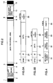
- Figs. 3A and 3B show the formats of blocks in different areas.
- Fig. 4 shows the format of ID information 21.
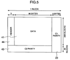
- Fig. 5 shows the format of data on one track in a data recording area 7.
- Fig. 6 is a block diagram of a modulating circuit 112.
- Fig. 7 is a block diagram of a scramble circuit 303.
- Fig. 8 is a block diagram of a precode circuit 300.
- Fig. 1 is a block diagram of a digital signal recording apparatus of one embodiment of the invention.
- rotating heads 100 a capstan 101
- a recording signal processing circuit 102 for generating a recording signal upon recording
- a control circuit 104 for controlling recording modes or the like, such as a microprocessor
- a timing generation circuit 105 for generating timing signals which control the operation of the rotating heads 100 and other operations
- a servo circuit 106 for controlling the head rotation and the tape transport speed
- an input circuit 107 for receiving the signal being recorded
- a timing control circuit 109 for controlling the recording timing
- an oscillation circuit 110 for generating a reference clock
- a tape 111 a tape 111
- modulating circuit 112 for the recording signal.
- Recording data in a packet format is fed to the input circuit 107 through an input/output terminal 108 at arbitrary intervals of time.
- a part of the packet data fed from the input/output terminal 108 is supplied through the input circuit 107 to the control circuit 104.
- the control circuit 104 detects the kind of the packet data, the maximum transmission rate and so on from the information added to the packet data or other information separately fed, decides a recording mode from the detected results, and fixes the modes in which the recording signal processing circuit 102 and servo circuit 106 are to be operated.
- the input circuit 107 detects the packet data to be recorded, and supplies it to the recording signal processing circuit 102.
- the recording signal processing circuit 102 decides the number of packets to be recorded on each track according to the recording mode decided by the control circuit 104, generates an error detection and correction code and so on, and generates the recording signal.
- the modulating circuit 112 modulates the recording signal, and the modulated signal is then recorded on the tape 111 by the rotating heads 100.
- Fig. 2 shows the format, or recording pattern, of the signal recorded on each track.
- the one-track pattern includes an auxiliary data recording area 3 for an audio signal and so on, a data recording area 7 for a digital compressed video signal, a sub-code recording area 12 for a sub-code such as time information and program information, preambles 2, 6 and 11 to those recording areas, postambles 4, 8 and 13 after those recording areas, gaps 5 and 9 between those recording areas, and margins 1 and 14 at the opposite ends of the track.
- the preambles, postambles and gaps provided before, after and between those recording areas make it possible to separately perform post-recording (or after-recording) on the respective areas.
- other digital signals than the digital compressed video signal and audio signal may be recorded on the recording areas 3 and 7.
- the digital compressed video signal and digital compressed audio signal may be recorded together on the areas 7.
- Figs. 3A and 3B show the block formats of those areas.
- Fig. 3A shows the block format of the auxiliary data recording area 3 and data recording area 7.
- this block includes a synchronizing signal 20, ID information 21, data 22 and a parity (C1 parity) for the first error detection and correction.
- the synchronizing signal 20, ID information 21, data 22, and parity 23 have 2 bytes, 3 bytes, 99 bytes and 8 bytes, respectively, to form one block of 112 bytes.
- Fig. 3B shows the block format of the sub-code recording area 12. This block includes the synchronizing signal 20 of 2 bytes, ID information of 3 bytes same as in Fig. 3A, data 22 of 19 bytes, and parity 23 of 4 bytes.
- one block corresponds to 1/4 the block length in Fig. 3A, or to 28 bytes.
- the ratio of the byte number of one block to the other becomes an integer, and since the structures of the synchronizing signal 20 and ID information 21 are the same throughout all the areas, respectively, the block generation and the detection of the synchronizing signal and ID information at the time of recording can be performed by the same circuit.
- Fig. 4 shows the format of the ID information 21.
- This ID information includes a sequence number 31, a track address 32, a block address 33 within each track, and a parity 35 for the detection of error in the sequence number 31, track address 32 and block address 33.
- the block address 33 is used for discriminating the blocks in each recording area. For example, it can be changed from 0 to 335 in the data recording area 7, from 0 to 13 in the auxiliary data recording area 3, and from 0 to 15 in the sub-code recording area 12.
- the track address 32 is used for discriminating the tracks. For example, it can be changed one from 0 to 5 for each track or from 0 to 2 for every two tracks, or totally 6 tracks can be discriminated by this track address.
- the sequence number 31 is changed from 0 to 11 for every six tracks discriminated by the track address 32, or totally 72 tracks can be discriminated by the sequence number 31. If the track address is synchronized with the period of the second error correction code which will be described later, the processing upon recording and the discrimination upon reproduction can be easily performed.
- Fig. 5 shows the format of data of each block in the data recording area 7.
- the data recording area 7 is formed of, for example, 336 blocks.
- Data 41 is recorded in the first 306 blocks, and the second error correction code (C2 parity) 43 in the other 30 blocks.
- the C2 parity 43 is added such that, for example, the C2 parity of 10 blocks is added to each 102 blocks into which data of 306 blocks ⁇ 6 tracks is divided by 18.
- the error correction code may be, for example, Reed-Solomon code.
- Data of 99 bytes of each block is formed of a header 44 of 3 bytes and data 41 of 96 bytes.
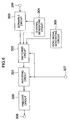
- Fig. 6 is a block diagram of the modulating circuit 112. Referring to Fig. 6, there are shown a precode circuit 300, an inverting circuit 301, a switching circuit 302, a scramble circuit 303, an ID signal 21 generating circuit 304, and a generating circuit 305 for generating a synchronizing signal 20.
- the data 22 and C1 parity 23 fed through an input terminal 306 are supplied to and scrambled by the scramble circuit 303 and then fed to the switching circuit 302.
- the switching circuit 302 is responsive to a predetermined timing signal that is generated from the timing generation circuit 105 and fed through an input terminal 307 to switch among the output from the scramble circuit 303, the ID signal generated from the ID signal generation circuit 304 and the synchronizing signal generated from the synchronizing signal generation circuit 305, and as a result produces the block signal shown in Figs. 3A and 3B.
- This block signal is processed by the precode circuit 300 after its ID signal is inverted by the inverting circuit 301.
- the precoded signal is then fed through an output terminal 308 to the rotating heads 100 by which it is recorded on the tape.
- Fig. 7 is a block diagram of the scramble circuit 303.
- This circuit arrangement includes an exclusive logic sum (OR) circuit 310 and a random number generation circuit 311 for generating, for example, a Maximum length sequence code, an input terminal 312 for receiving input data, an output terminal 313, and an input terminal 314.
- the block address 33 and track address 32 generated from the ID signal generating circuit 304 and received by the terminal 314 are fed to the random number generating circuit 311 as initial values.
- the generated random number from the generator is added to the data 22 and C1 parity 23.
- Fig. 8 is a block diagram of the precode circuit 300.
- This circuit arrangement includes one-bit delay circuits 320 and the exclusive logic sum circuit 310.
- the input data fed through an input terminal 321 and a signal delayed two bits relative to the input data are exclusive-ORed to produce a precoded signal.
- the output at an output terminal 322 is also a succession of "0"s. If the input data contains "1”, the output is sure to be inverted. If the input data is a succession of "1"s, the output becomes a repetition of 1100.
- the ID signal 21 is not scrambled. Therefore, the head of the sequence is always "0".
- the parity 35 is a simple parity, "0" continuously appears over 24 bits. Even when the parity 35 is a special one, "0" continuously appears over 16 bits.
- the track address 32 and block address 33 periodically take “0".
- the ID signal is directly precoded, it is likely that a run-length of 24 bits maximum is caused in the recording signal depending on the values of delay circuits 320. However, if the precode processing is made after the inversion of the ID signal, such a long run-length does not occur.
- the other scrambled signal than the ID signal may be similarly precoded and recorded after being inverted.
- the non-scrambled information is precoded after inversion, it is possible to reduce the possibility of a long run-length pattern occurring in the recording signal.
Landscapes
- Engineering & Computer Science (AREA)
- Signal Processing (AREA)
- Multimedia (AREA)
- Signal Processing For Digital Recording And Reproducing (AREA)
- Television Signal Processing For Recording (AREA)
- Digital Magnetic Recording (AREA)
Applications Claiming Priority (3)
| Application Number | Priority Date | Filing Date | Title |
|---|---|---|---|
| JP6914195 | 1995-03-28 | ||
| JP69141/95 | 1995-03-28 | ||
| JP7069141A JP2897679B2 (ja) | 1995-03-28 | 1995-03-28 | ディジタル信号記録装置 |
Publications (3)
| Publication Number | Publication Date |
|---|---|
| EP0735536A2 true EP0735536A2 (fr) | 1996-10-02 |
| EP0735536A3 EP0735536A3 (fr) | 1997-07-23 |
| EP0735536B1 EP0735536B1 (fr) | 2001-01-17 |
Family
ID=13394081
Family Applications (1)
| Application Number | Title | Priority Date | Filing Date |
|---|---|---|---|
| EP96104729A Expired - Lifetime EP0735536B1 (fr) | 1995-03-28 | 1996-03-25 | Appareil et méthode d'enregistrement de signaux digitaux |
Country Status (5)
| Country | Link |
|---|---|
| US (1) | US5815331A (fr) |
| EP (1) | EP0735536B1 (fr) |
| JP (1) | JP2897679B2 (fr) |
| KR (1) | KR100204722B1 (fr) |
| DE (1) | DE69611564T2 (fr) |
Families Citing this family (1)
| Publication number | Priority date | Publication date | Assignee | Title |
|---|---|---|---|---|
| JP4147607B2 (ja) * | 1998-03-13 | 2008-09-10 | 松下電器産業株式会社 | 補助スクランブル/デスクランブル方法および装置 |
Citations (6)
| Publication number | Priority date | Publication date | Assignee | Title |
|---|---|---|---|---|
| JPS60256984A (ja) * | 1984-05-31 | 1985-12-18 | Nec Corp | 磁気記録再生装置 |
| EP0343930A2 (fr) * | 1988-05-24 | 1989-11-29 | Sony Corporation | Appareil de traitement de signaux de données |
| US4885646A (en) * | 1987-10-15 | 1989-12-05 | Sony Corporation | Digital recorder using partial response method |
| EP0388031A2 (fr) * | 1989-03-13 | 1990-09-19 | International Business Machines Corporation | Modification de la fiabilité d'un dispositif de stockage de données non volatiles sur une piste |
| JPH02252334A (ja) * | 1989-03-27 | 1990-10-11 | Sony Corp | 選択的スクランブル回路 |
| EP0686968A2 (fr) * | 1994-06-07 | 1995-12-13 | Matsushita Electric Industrial Co., Ltd. | Milieu d'enregistrement d'information optique, méthode d'enregistrement d'information optique, et appareil de reproduction d'information optique |
Family Cites Families (4)
| Publication number | Priority date | Publication date | Assignee | Title |
|---|---|---|---|---|
| US4680791A (en) * | 1984-05-31 | 1987-07-14 | Nec Corporation | Digital video signal process apparatus for use in a video tape recorder |
| JPH0721942B2 (ja) * | 1984-10-11 | 1995-03-08 | ソニー株式会社 | チヤンネル符号化方法 |
| JP2848001B2 (ja) * | 1990-10-31 | 1999-01-20 | ソニー株式会社 | ディジタルデータの磁気記録装置 |
| JP3237152B2 (ja) * | 1991-11-15 | 2001-12-10 | ソニー株式会社 | ディジタル情報信号の記録装置 |
-
1995
- 1995-03-28 JP JP7069141A patent/JP2897679B2/ja not_active Expired - Fee Related
-
1996
- 1996-03-21 US US08/620,687 patent/US5815331A/en not_active Expired - Lifetime
- 1996-03-25 DE DE69611564T patent/DE69611564T2/de not_active Expired - Fee Related
- 1996-03-25 EP EP96104729A patent/EP0735536B1/fr not_active Expired - Lifetime
- 1996-03-27 KR KR1019960008487A patent/KR100204722B1/ko not_active IP Right Cessation
Patent Citations (6)
| Publication number | Priority date | Publication date | Assignee | Title |
|---|---|---|---|---|
| JPS60256984A (ja) * | 1984-05-31 | 1985-12-18 | Nec Corp | 磁気記録再生装置 |
| US4885646A (en) * | 1987-10-15 | 1989-12-05 | Sony Corporation | Digital recorder using partial response method |
| EP0343930A2 (fr) * | 1988-05-24 | 1989-11-29 | Sony Corporation | Appareil de traitement de signaux de données |
| EP0388031A2 (fr) * | 1989-03-13 | 1990-09-19 | International Business Machines Corporation | Modification de la fiabilité d'un dispositif de stockage de données non volatiles sur une piste |
| JPH02252334A (ja) * | 1989-03-27 | 1990-10-11 | Sony Corp | 選択的スクランブル回路 |
| EP0686968A2 (fr) * | 1994-06-07 | 1995-12-13 | Matsushita Electric Industrial Co., Ltd. | Milieu d'enregistrement d'information optique, méthode d'enregistrement d'information optique, et appareil de reproduction d'information optique |
Non-Patent Citations (2)
| Title |
|---|
| PATENT ABSTRACTS OF JAPAN vol. 010, no. 135 (P-457), 20 May 1986 & JP 60 256984 A (NIPPON DENKI KK), 18 December 1985, * |
| PATENT ABSTRACTS OF JAPAN vol. 014, no. 580 (E-1017), 25 December 1990 & JP 02 252334 A (SONY CORP), 11 October 1990, * |
Also Published As
| Publication number | Publication date |
|---|---|
| JPH08273300A (ja) | 1996-10-18 |
| KR960035437A (ko) | 1996-10-24 |
| KR100204722B1 (ko) | 1999-06-15 |
| EP0735536B1 (fr) | 2001-01-17 |
| DE69611564T2 (de) | 2001-08-23 |
| DE69611564D1 (de) | 2001-02-22 |
| JP2897679B2 (ja) | 1999-05-31 |
| US5815331A (en) | 1998-09-29 |
| EP0735536A3 (fr) | 1997-07-23 |
Similar Documents
| Publication | Publication Date | Title |
|---|---|---|
| EP0343930B1 (fr) | Appareil de traitement de signaux de données | |
| US6046872A (en) | Method and apparatus for recording digital signal | |
| KR100387460B1 (ko) | 기록장치및방법,기록매체,재생장치 | |
| US7450816B2 (en) | Digital signal recording and reproduction apparatus suitable for recording and reproducing a compressed video signal | |
| USRE36096E (en) | Arrangement for recording clock run-in codewords at the beginning of a track on a magnetic record carrier | |
| JPH02203474A (ja) | 情報信号の記録再生方法及び記録再生装置 | |
| US4577180A (en) | Digital data converting method and apparatus thereof | |
| US4680791A (en) | Digital video signal process apparatus for use in a video tape recorder | |
| US5815331A (en) | Digital signal recording method and apparatus involving precode processing for partial response detection | |
| EP0425475B1 (fr) | Système de transmission et de détection de données | |
| EP0794531A2 (fr) | Appareil d'enregistrement/reproduction de signaux digitaux et méthode d'enregistrement | |
| JPH0666944B2 (ja) | 映像信号再生装置 | |
| EP0336624B1 (fr) | Appareil de reproduction de données | |
| JP2947081B2 (ja) | デジタル情報変調装置 | |
| EP0915465B1 (fr) | Appareil pour enregistrer des signaux numériques, et procédé associé | |
| US5856798A (en) | Magnetic-tape recording/reproducing arrangement comprising a coding device | |
| JPS5823309A (ja) | デスクランブル回路 | |
| JP2898132B2 (ja) | ディジタル変調方法および装置 | |
| JPH0574146B2 (fr) | ||
| JPH05109202A (ja) | デイジタル記録再生装置 | |
| JP2512168B2 (ja) | ディジタル信号磁気記録再生装置 | |
| JP2870502B2 (ja) | ディジタルデータの復調装置 | |
| JP3008882B2 (ja) | ディジタル情報受信記録再生置 | |
| JPH07101544B2 (ja) | 誤り検出装置 | |
| JPH04366471A (ja) | Mスクランブル回路 |
Legal Events
| Date | Code | Title | Description |
|---|---|---|---|
| PUAI | Public reference made under article 153(3) epc to a published international application that has entered the european phase |
Free format text: ORIGINAL CODE: 0009012 |
|
| 17P | Request for examination filed |
Effective date: 19960326 |
|
| AK | Designated contracting states |
Kind code of ref document: A2 Designated state(s): DE FR GB |
|
| PUAL | Search report despatched |
Free format text: ORIGINAL CODE: 0009013 |
|
| AK | Designated contracting states |
Kind code of ref document: A3 Designated state(s): DE FR GB |
|
| 17Q | First examination report despatched |
Effective date: 19981020 |
|
| GRAG | Despatch of communication of intention to grant |
Free format text: ORIGINAL CODE: EPIDOS AGRA |
|
| 17Q | First examination report despatched |
Effective date: 19981020 |
|
| GRAG | Despatch of communication of intention to grant |
Free format text: ORIGINAL CODE: EPIDOS AGRA |
|
| GRAG | Despatch of communication of intention to grant |
Free format text: ORIGINAL CODE: EPIDOS AGRA |
|
| GRAH | Despatch of communication of intention to grant a patent |
Free format text: ORIGINAL CODE: EPIDOS IGRA |
|
| GRAH | Despatch of communication of intention to grant a patent |
Free format text: ORIGINAL CODE: EPIDOS IGRA |
|
| GRAA | (expected) grant |
Free format text: ORIGINAL CODE: 0009210 |
|
| AK | Designated contracting states |
Kind code of ref document: B1 Designated state(s): DE FR GB |
|
| REF | Corresponds to: |
Ref document number: 69611564 Country of ref document: DE Date of ref document: 20010222 |
|
| ET | Fr: translation filed | ||
| PLBE | No opposition filed within time limit |
Free format text: ORIGINAL CODE: 0009261 |
|
| STAA | Information on the status of an ep patent application or granted ep patent |
Free format text: STATUS: NO OPPOSITION FILED WITHIN TIME LIMIT |
|
| REG | Reference to a national code |
Ref country code: GB Ref legal event code: IF02 |
|
| 26N | No opposition filed | ||
| PGFP | Annual fee paid to national office [announced via postgrant information from national office to epo] |
Ref country code: FR Payment date: 20050222 Year of fee payment: 10 |
|
| PGFP | Annual fee paid to national office [announced via postgrant information from national office to epo] |
Ref country code: GB Payment date: 20050228 Year of fee payment: 10 |
|
| PGFP | Annual fee paid to national office [announced via postgrant information from national office to epo] |
Ref country code: DE Payment date: 20050304 Year of fee payment: 10 |
|
| PG25 | Lapsed in a contracting state [announced via postgrant information from national office to epo] |
Ref country code: GB Free format text: LAPSE BECAUSE OF NON-PAYMENT OF DUE FEES Effective date: 20060325 |
|
| PG25 | Lapsed in a contracting state [announced via postgrant information from national office to epo] |
Ref country code: DE Free format text: LAPSE BECAUSE OF NON-PAYMENT OF DUE FEES Effective date: 20061003 |
|
| GBPC | Gb: european patent ceased through non-payment of renewal fee |
Effective date: 20060325 |
|
| REG | Reference to a national code |
Ref country code: FR Ref legal event code: ST Effective date: 20061130 |
|
| PG25 | Lapsed in a contracting state [announced via postgrant information from national office to epo] |
Ref country code: FR Free format text: LAPSE BECAUSE OF NON-PAYMENT OF DUE FEES Effective date: 20060331 |