EP0734079A2 - Verfahren zum Aufwachsen aus der Gasphase - Google Patents
Verfahren zum Aufwachsen aus der Gasphase Download PDFInfo
- Publication number
- EP0734079A2 EP0734079A2 EP96301977A EP96301977A EP0734079A2 EP 0734079 A2 EP0734079 A2 EP 0734079A2 EP 96301977 A EP96301977 A EP 96301977A EP 96301977 A EP96301977 A EP 96301977A EP 0734079 A2 EP0734079 A2 EP 0734079A2
- Authority
- EP
- European Patent Office
- Prior art keywords
- vapor
- thickness
- single crystal
- gaas
- substrates
- Prior art date
- Legal status (The legal status is an assumption and is not a legal conclusion. Google has not performed a legal analysis and makes no representation as to the accuracy of the status listed.)
- Granted
Links
Images

Classifications
-
- H—ELECTRICITY
- H10—SEMICONDUCTOR DEVICES; ELECTRIC SOLID-STATE DEVICES NOT OTHERWISE PROVIDED FOR
- H10P—GENERIC PROCESSES OR APPARATUS FOR THE MANUFACTURE OR TREATMENT OF DEVICES COVERED BY CLASS H10
- H10P14/00—Formation of materials, e.g. in the shape of layers or pillars
- H10P14/20—Formation of materials, e.g. in the shape of layers or pillars of semiconductor materials
- H10P14/29—Formation of materials, e.g. in the shape of layers or pillars of semiconductor materials characterised by the substrates
- H10P14/2901—Materials
- H10P14/2907—Materials being Group IIIA-VA materials
- H10P14/2909—Phosphides
-
- H—ELECTRICITY
- H10—SEMICONDUCTOR DEVICES; ELECTRIC SOLID-STATE DEVICES NOT OTHERWISE PROVIDED FOR
- H10H—INORGANIC LIGHT-EMITTING SEMICONDUCTOR DEVICES HAVING POTENTIAL BARRIERS
- H10H20/00—Individual inorganic light-emitting semiconductor devices having potential barriers, e.g. light-emitting diodes [LED]
- H10H20/01—Manufacture or treatment
- H10H20/011—Manufacture or treatment of bodies, e.g. forming semiconductor layers
- H10H20/013—Manufacture or treatment of bodies, e.g. forming semiconductor layers having light-emitting regions comprising only Group III-V materials
-
- H—ELECTRICITY
- H10—SEMICONDUCTOR DEVICES; ELECTRIC SOLID-STATE DEVICES NOT OTHERWISE PROVIDED FOR
- H10P—GENERIC PROCESSES OR APPARATUS FOR THE MANUFACTURE OR TREATMENT OF DEVICES COVERED BY CLASS H10
- H10P14/00—Formation of materials, e.g. in the shape of layers or pillars
- H10P14/20—Formation of materials, e.g. in the shape of layers or pillars of semiconductor materials
- H10P14/24—Formation of materials, e.g. in the shape of layers or pillars of semiconductor materials using chemical vapour deposition [CVD]
-
- H—ELECTRICITY
- H10—SEMICONDUCTOR DEVICES; ELECTRIC SOLID-STATE DEVICES NOT OTHERWISE PROVIDED FOR
- H10P—GENERIC PROCESSES OR APPARATUS FOR THE MANUFACTURE OR TREATMENT OF DEVICES COVERED BY CLASS H10
- H10P14/00—Formation of materials, e.g. in the shape of layers or pillars
- H10P14/20—Formation of materials, e.g. in the shape of layers or pillars of semiconductor materials
- H10P14/29—Formation of materials, e.g. in the shape of layers or pillars of semiconductor materials characterised by the substrates
- H10P14/2901—Materials
- H10P14/2907—Materials being Group IIIA-VA materials
- H10P14/2911—Arsenides
-
- H—ELECTRICITY
- H10—SEMICONDUCTOR DEVICES; ELECTRIC SOLID-STATE DEVICES NOT OTHERWISE PROVIDED FOR
- H10P—GENERIC PROCESSES OR APPARATUS FOR THE MANUFACTURE OR TREATMENT OF DEVICES COVERED BY CLASS H10
- H10P14/00—Formation of materials, e.g. in the shape of layers or pillars
- H10P14/20—Formation of materials, e.g. in the shape of layers or pillars of semiconductor materials
- H10P14/32—Formation of materials, e.g. in the shape of layers or pillars of semiconductor materials characterised by intermediate layers between substrates and deposited layers
- H10P14/3202—Materials thereof
- H10P14/3214—Materials thereof being Group IIIA-VA semiconductors
- H10P14/3218—Phosphides
-
- H—ELECTRICITY
- H10—SEMICONDUCTOR DEVICES; ELECTRIC SOLID-STATE DEVICES NOT OTHERWISE PROVIDED FOR
- H10P—GENERIC PROCESSES OR APPARATUS FOR THE MANUFACTURE OR TREATMENT OF DEVICES COVERED BY CLASS H10
- H10P14/00—Formation of materials, e.g. in the shape of layers or pillars
- H10P14/20—Formation of materials, e.g. in the shape of layers or pillars of semiconductor materials
- H10P14/32—Formation of materials, e.g. in the shape of layers or pillars of semiconductor materials characterised by intermediate layers between substrates and deposited layers
- H10P14/3202—Materials thereof
- H10P14/3214—Materials thereof being Group IIIA-VA semiconductors
- H10P14/3221—Arsenides
-
- H—ELECTRICITY
- H10—SEMICONDUCTOR DEVICES; ELECTRIC SOLID-STATE DEVICES NOT OTHERWISE PROVIDED FOR
- H10P—GENERIC PROCESSES OR APPARATUS FOR THE MANUFACTURE OR TREATMENT OF DEVICES COVERED BY CLASS H10
- H10P14/00—Formation of materials, e.g. in the shape of layers or pillars
- H10P14/20—Formation of materials, e.g. in the shape of layers or pillars of semiconductor materials
- H10P14/34—Deposited materials, e.g. layers
- H10P14/3402—Deposited materials, e.g. layers characterised by the chemical composition
- H10P14/3414—Deposited materials, e.g. layers characterised by the chemical composition being group IIIA-VIA materials
- H10P14/3418—Phosphides
-
- H—ELECTRICITY
- H10—SEMICONDUCTOR DEVICES; ELECTRIC SOLID-STATE DEVICES NOT OTHERWISE PROVIDED FOR
- H10P—GENERIC PROCESSES OR APPARATUS FOR THE MANUFACTURE OR TREATMENT OF DEVICES COVERED BY CLASS H10
- H10P14/00—Formation of materials, e.g. in the shape of layers or pillars
- H10P14/20—Formation of materials, e.g. in the shape of layers or pillars of semiconductor materials
- H10P14/34—Deposited materials, e.g. layers
- H10P14/3402—Deposited materials, e.g. layers characterised by the chemical composition
- H10P14/3414—Deposited materials, e.g. layers characterised by the chemical composition being group IIIA-VIA materials
- H10P14/3421—Arsenides
-
- Y—GENERAL TAGGING OF NEW TECHNOLOGICAL DEVELOPMENTS; GENERAL TAGGING OF CROSS-SECTIONAL TECHNOLOGIES SPANNING OVER SEVERAL SECTIONS OF THE IPC; TECHNICAL SUBJECTS COVERED BY FORMER USPC CROSS-REFERENCE ART COLLECTIONS [XRACs] AND DIGESTS
- Y10—TECHNICAL SUBJECTS COVERED BY FORMER USPC
- Y10S—TECHNICAL SUBJECTS COVERED BY FORMER USPC CROSS-REFERENCE ART COLLECTIONS [XRACs] AND DIGESTS
- Y10S117/00—Single-crystal, oriented-crystal, and epitaxy growth processes; non-coating apparatus therefor
- Y10S117/901—Levitation, reduced gravity, microgravity, space
- Y10S117/902—Specified orientation, shape, crystallography, or size of seed or substrate
Definitions
- This invention relates to a method for a vapor-phase growth of an epitaxial layer(s) of a compound semiconductor and more particularly to a method for a vapor-phase growth of a GaAS 1-x P x epitaxial layer (wherein x stands for a composition in the range, 0 ⁇ x ⁇ 1).
- the GaAsP epitaxial wafer obtained by forming a GaAs 1-x P x epitaxial layer(s) (wherein x stands for an alloy composition in the range, 0 ⁇ x ⁇ 1) on a GaP or a GaAs single crystal substrate is used for a yellow to red light-emitting diode.
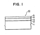
- the GaAsP epitaxial wafer mentioned above has such a sectional structure as shown in Fig. 1, in which 1 stands for an n-type Gap single crystal substrate of 300 ⁇ m in thickness, 2 to 5 for epitaxially grown layers having a total thickness of 50 ⁇ m, specifically 2 for an n-type GaP layer of 3 ⁇ m in thickness, 3 for an n-type GaAs 1-x P x graded layer having the GaP alloy composition x, decreased from 1 to a necessary value of x (x 0 ) and a thickness of 25 ⁇ m, 4 for a n-type GaAs 1-x P x composition constant layer having the alloy composition, x, constant at x 0 and a thickness of 8 ⁇ m, and 5 for a nitrogen-doped n-type GaAs 1-x P x composition constant layer having the alloy composition, x, constant at x 0 and a thickness of 14 ⁇ m.
- the GaasP light-emitting diode is obtained by diffusing Zn into the aforementioned GaAaP epitaxial wafer 10 through the obverse surface side of the nitrogen-doped n-type GaAs 1-x P x composition constant layer 5 thereby giving rise to a p-n junction having a p-type diffused layer of 4 to 5 ⁇ m in thickness and, thereafter, dicing to a necessary configuration.
- the nitrogen-doped n-type GaAs 1-x P x composition constant layer 5 emits light of a wavelength which is corresponding to the GaP alloy composition, x.
- the GaAsP epitaxial wafer mentioned above is generally produced by a method of vapor-phase epitaxial growth, hereinafter referred to as "method for vapor-phase growth", such as, for example, the method of the hydride type vaporphase growth.
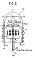
- the GaAsP epitaxial wafer(s) is obtained by setting the n-type single crystal substrate(s) on a wafer holder 16 inside a vapor-phase growth apparatus 30, using phosphine (PH 3 ), arsine (ASH 3 ), and hydrogen chloride (HCl; providing HCl which reacts with Ga 17 in a Ga storage vessel 14 to form GaCl) as source gases, hydrogen sulfide (H 2 S) as an n-type dopant source, ammonia (NH 3 ) as a nitrogen source, and hydrogen (H 2 ) as a carrier gas, and feeding these gases by setting amounts and temperatures in accordance with the GaP alloy composition, x (for a composition satisfying the expression, 0 ⁇ x ⁇ 1) mentioned above thereby sequentially forming the epitaxially grown layers 2, 3, 4, and 5 in the order on the n-type GaP single crystal substrate 1.
- phosphine PH 3
- arsine arsine
- HCl hydrogen chloride
- H 2 S
- the GaAsP epitaxial wafer has been produced by the method described above with the amount of the n-type GaP single crystal substrate 1, or the n-type GaAs single crystal substrate) 1, placed on the wafer holder 16 at a covering level in a range of 55 to 60% as the ratio of the total area of the substrate to the area of the wafer holder 16, hereinafter referred to as "covering ratio of substrate”.
- the covering ratio of substrate is in the range of 55 to 60%, however, the total thickness of the epitaxially grown layers in the central part and the total thickness of the epitaxially grown layers in the peripheral part of a GaAsP epitaxial wafer 10' inevitably produce a difference of about 2 times in the ratio of these total thicknesses as shown in Fig. 3.
- the GaAsP epitaxial wafer involving such a large dispersion in the total thickness of epitaxially grown layers as mentioned above (also involving a similarly large dispersion in the thickness of the GaAsP epitaxial wafer) is used as a substrate for a GaAsP light-emitting diode, the following problems are entailed.
- the large dispersion of thickness in the individual wafers (1) forms the cause of a large decrease in the yield during the process of manufacture of light-emitting diode chips, hereinafter referred to as "LED chips", and (2), owing to the large difference in total thickness (height) in the individual LED chips, causes troubles in the process of assemblage by the use of an automated device, suffer an increased loss of process time, and induce a decrease in the yield of the process of assemblage.
- the large dispersion of total thickness of the epitaxially grown layers mentioned above (1) causes a large dispersion of a forward voltage (V F ) and particularly aggravates the defect of this voltage, V F , in those light-emitting diodes which originate in -the peripheral part of a wafer and (2) impairs the uniformity of the luminance and the color of the light to be emitted.
- V F forward voltage
- GaAsP epitaxial wafer which comprise epitaxially grown layers having a uniform total thickness ([largest thickness in the whole area of wafer]/[smallest thickness in the whole area of wafer] ⁇ 1.5) has been desired.
- This invention is directed to the production of a GaAsP epitaxial wafer and has for an object thereof the provision of a method for the vapor-phase growth which obtains a GaAs 1-x P x epitaxial layer(s) (wherein x stands for an alloy composition satisfying the expression, 0 ⁇ x ⁇ 1) having a uniform thickness.
- this invention provides a method for a vapor-phase growth comprising the steps of setting a plurality of semiconductor single crystal substrates in place on a wafer holder disposed in a vapor-phase growth apparatus and forming a GaAs 1-x P x epitaxial layers(s) (0 ⁇ x ⁇ 1) on the semiconductor single crystal substrates by means of vapor-phase growth, characterized in that a covering ratio of a total surface area of charged semiconductor single crystal substrates to the surface area of a wafer holder is not less than 70%.
- the material for the wafer holder mentioned above is selected from carbon or quartz, and the single crystal as the material for the semiconductor single crystal substrates is selected from GaP or GaAs.
- GaAs 1-x P x epitaxial layer(s) (0 ⁇ x ⁇ 1) is formed by vapor-phase growth on the substrates
- virtually no GaAs 1-x P x (0 ⁇ x ⁇ 1) is deposited on the surface of the wafer holder because the activation energy of the reaction for the growth of GaAs 1-x P x on the surface of the wafer holder is extremely large as compared with that on the surface of the substrates [inclusive of a surface of the GaAs 1-x P x epitaxial layer (0 ⁇ x ⁇ 1) formed by the vapor-phase growth].
- the concentration of the source gases (GaCl and P 4 formed by decomposition of PH 3 and/or As 4 formed by decomposition of AsH 3 ) flowing on the substrates therefore, is abnormally high in the peripheral part of the substrates as compared with that in the central part thereof. As a result, conspicuous lack of uniformity occurs in the thickness of the epitaxial layer(s) as shown in Fig. 3.
- the present inventors have continued a diligent study based on the knowledge mentioned above and consequently found that the GaAs 1-x P x epitaxial layer(s) can be formed in a uniform thickness by vapor-phase growth by increasing the covering ratio of the substrates mentioned above.
- the amount of the semiconductor single crystal substrates to be charged for vapor-phase growth is set at a level of not less than 70% as the covering ratio of the total surface area to the surface area of the wafer holder, the phenomenon that the concentration of source gases is unduly heightened in the peripheral part of the substrates as cmpared with that in the central part thereof and the uniformity of thickness of the epitaxial layer(s) is impaired because the activation energy of the reaction for the growth of the GaAs 1-x P x is extremely large on the surface of the wafer holder as compared with that on the surface of the substrates can be inhibited.
- the augmented uniformity of the thickness of the epitaxial layer(s) results in decreasing the dispersion of wafer thickness, (1) increasing the yield of the process of production of LED chips, (2) uniformizing the thickness of LED chips, diminishing the troubles incurred during the process of assemblage of LED chips by an automated device, decreasing the time loss of this process, and further improving the yield of the process of assemblage.
- the uniformization of the thickness of the epitaxial layer(s) mentioned above results in (1) diminishing the dispersion of the forward voltage (V F ) and (2) uniformizing the luminance and the color of the light to be emitted.
- Fig. 1 is a sectioned structural diagram of a GaAsP epitaxial wafer.
- Fig. 2 is a schematic structural diagram of a vapor-phase growth apparatus to be used for the production of a GaAsP epitaxial wafer of the example.
- Fig. 3 is a sectioned structural diagram of a GaAsP epitaxial wafer to be obtained by a conventional method for vapor-phase growth.
- GaAsP epitaxial wafers (GaAsP epitaxial wafers for yellow light-emitting diodes in this example) of a structure shown in Fig. 1 were produced as follows.
- Fig. 2 is a schematic structural diagram of a vapor-phase growth apparatus used for the production of the GaAsP epitaxial wafers of this example.
- 1 stands for an n-type GaP single crystal substrate, 11 for a quartz bell jar, 12 for a high-frequency induction heating coil, 13 for a high-frequency susceptor, 14 for a Ga storing vessel, 15 for a gas mixer, 16 for a wafer holder, 17 for Ga, 18 for a carrier gas (H 2 ) inlet, 19 for an HCl inlet, 20 for an inlet for PH 3 , AsH 3 , H 2 S, and NH 3 gases, and 21 for a gas outlet.
- H 2 carrier gas
- a mirror-polished wafer having a surface off-angled by 10° from the plane of ⁇ 100 ⁇ to the direction of ⁇ 110> as a main surface, a thickness of 300 ⁇ m, and a Te impurity concentration in the range of 2 to 4 x 10 17 atoms/cm 3 were used as the n-type GaP single crystal substrate 1.
- the gases used for the vapor-phase growth were hydrogen (H 2 ), hydrogen sulfide (H 2 S) diluted with H 2 to a concentration of 50 ppm, arsine (AsH 3 ) diluted with H 2 to a concentration of 1%, phosphine (PH 3 ) diluted with H 2 to a concentration of 10%, hydrogen chloride (HCl) of a high purity, and ammonia gas (NH 3 ).
- H 2 hydrogen
- H 2 S hydrogen sulfide
- AsH 3 arsine
- PH 3 phosphine
- NH 3 ammonia gas
- the n-type GaP single crystal substrates 1 were set in place on the wafer holder 16 disposed inside the vapor-phase growth apparatus 30 at a covering ratio (the ratio of the total surface area of the substrates 1 charged to the surface area of the wafer holder) of 80%.
- Nitrogen gas (N 2 ) and then hydrogen gas (H 2 ) as a carrier gas were introduced into the vapor-phase growth apparatus 30 until thorough displacement of the interior of the growth apparatus 30. Then, the growth apparatus 30 was heated until the temperature of the substrates 1 reached to 860°C. Subsequently, vapor-phase growth of a GaAs 1-x P x epitaxial layer for yellow-color light emission was started.
- the H 2 S/H 2 was introduced at a flow volume of 10 cc/minute
- the HCl was introduced meanwhile at a flow volume of 45 cc/minute and caused to react with the Ga 17 in the Ga storage vessel 14 to give birth to GaCl
- the PH 3 /H 2 was introduced simultaniously at a flow volume of 250 cc/minute to induce growth of the n-type GaP layer 2 in a target thickness of 3 pm on the n-type GaP single crystal substrates 1.
- the n-type GaAs 1-x P x of a graded layer 3 was grown to a target thickness of 25 ⁇ m by the following procedure.
- the GaP alloy composition ratio x was decreased from 1 to 0.85 by introducing the H 2 S/H 2 , HCl, and PH 3 /H 2 at respective fixed flow volumes of 10 cc/minute, 45 cc/minute, and 250 cc/minute and the ASH 3 /H 2 at a flow volume gradually increased from 0 cc/minute to 260 cc/minute. Meanwhile, the temperature of the substrates 1 was decreased from 860°C to 830°C.
- the n-type GaAs 1-x P x graded layer 3 having an alloy composition varied from GaP to GaAS 0.15 P 0.85 was grown on the n-type GaP layer 2 mentioned above.
- the H 2 S/H 2 , HCl, PH 3 /H 2 , and ASH 3 /H 2 were introduced at respective flow volumes of 10 cc/minute, 45 cc/minute, 250 cc/minute, and 260 cc/minute to attain growth of the n-type GaAs 0.15 P 0.85 composition constant layer 4 to a target thickness of 8 ⁇ m.
- the NH 3 was introduced at a flow volume of 400 cc/minute to effect growth of a nitrogen-doped n-type GaAs 0.15 P 0.85 composition constant layer 5, to a target thickness of 14 ⁇ m and complete the production of the GaAsP epitaxial wafer for a yellow light-emitting diode.
- the total thickness of the epitaxially grown layers of the GaAsP epitaxial wafers produced as described above were measured. The results are shown in Table 1.
- GaAsP epitaxial wafers for yellow light-emitting diodes were produced by following the procedure of Example 1 while setting the covering ratio of the substrates at 70%. The total thickness of the epitaxially grown layers were measured in the same manner as in Example 1. The results are also shown in Table 1.
- GaAsP epitaxial wafers for yellow light-emitting diodes were produced by following the procedure of Example 1 while setting the covering ratios of substrates at 55% (Comparative Example 1) and 60% (Comparative Example 2).
- the total thickness of the component epitaxially grown layers were measured in the same manner as in Example 1. The results are also shown in Table 1.
- Table 1 Covering ratio of substrates (%) Thickness of epitaxial layers ( ⁇ m)* Maximum value Minimum value Minimum value (Central part) Maximum value (Peripheral part)
- Example 1 80 50.3 65.4 1.30
- Max/Min The ratios of [maximum thickness in wafer]/[minimum thickness in wafer] (hereinafter referred to as Max/Min) were 1.30 and 1.46 respectively when the covering ratio of substrates were set at 80% (Example 1) and 70% (Example 2). These values are smaller than the target maximum of 1.5. This fact indicates that the magnitudes of dispersion of layer thickness were smaller than the tolerable maximum level.
- the increase of the covering ratio of substrates from 70% to 80% resulted in decreasing the Max/Min indicative of the magnitude of dispersion of thickness of the epitaxial layers from 1.46 to 1.30 and better the uniformity of thickness of the epitaxial layer(s). It is further noted that the covering ratio of substrates which satisfies the target uniformity of dispersion of layer thickness (Max/Min ⁇ 1.5) is not less than 70%.
- the examples further represent cases of using a GaP single crystal substrates as the substrates. Similarly satisfactory results are obtained when GaAs single crystal substrates are used instead.
- this invention uniformizes the concentration of source gases flowing on the central part and on the peripheral part of the substrates and consequently makes better the uniformity of the epitaxial layer(s) by setting the amount of charging of the semiconductor single crystal substrates at a level of not less than 70% as the covering ratio of the total surface area of the semiconductor single crystal substrates to the surface area of the wafer holder and consequently decreasing the ratio of the surface of the holder on which the reaction for epitaxial deposition does not occur.
- the better uniformity of the thickness of the epitaxial layer(s) results in decreasing the dispersion of wafer thickness, (1) increasing the yield of the process of production of LED chips, (2) uniformizing the thickness of LED chips, diminishing the troubles incurred during the process of assemblage of LED chips by an automated device, decreasing the time loss of this process, and further improving the yield of the process of assemblage.
- the uniformization of the thickness of the epitaxial layer(s) mentioned above results in (1) diminishing the dispersion of the forward voltage (V F ) and (2) uniformizing the luminance and the color of the light to be emitted.
Landscapes
- Led Devices (AREA)
- Recrystallisation Techniques (AREA)
Applications Claiming Priority (4)
| Application Number | Priority Date | Filing Date | Title |
|---|---|---|---|
| JP9133795 | 1995-03-24 | ||
| JP91337/95 | 1995-03-24 | ||
| JP9133795A JPH08264464A (ja) | 1995-03-24 | 1995-03-24 | 気相成長方法 |
| US08/619,294 US5759264A (en) | 1995-03-24 | 1996-03-21 | Method for vapor-phase growth |
Publications (3)
| Publication Number | Publication Date |
|---|---|
| EP0734079A2 true EP0734079A2 (de) | 1996-09-25 |
| EP0734079A3 EP0734079A3 (de) | 1998-03-25 |
| EP0734079B1 EP0734079B1 (de) | 2001-08-08 |
Family
ID=26432789
Family Applications (1)
| Application Number | Title | Priority Date | Filing Date |
|---|---|---|---|
| EP96301977A Expired - Lifetime EP0734079B1 (de) | 1995-03-24 | 1996-03-22 | Verfahren zum Aufwachsen aus der Gasphase |
Country Status (3)
| Country | Link |
|---|---|
| US (1) | US5759264A (de) |
| EP (1) | EP0734079B1 (de) |
| JP (1) | JPH08264464A (de) |
Cited By (1)
| Publication number | Priority date | Publication date | Assignee | Title |
|---|---|---|---|---|
| CN114108080A (zh) * | 2021-09-30 | 2022-03-01 | 华灿光电(浙江)有限公司 | 石墨基板、以及石墨基板和发光二极管外延片的制造方法 |
Families Citing this family (5)
| Publication number | Priority date | Publication date | Assignee | Title |
|---|---|---|---|---|
| JP3854693B2 (ja) * | 1996-09-30 | 2006-12-06 | キヤノン株式会社 | 半導体レーザの製造方法 |
| US6217662B1 (en) * | 1997-03-24 | 2001-04-17 | Cree, Inc. | Susceptor designs for silicon carbide thin films |
| JP3301371B2 (ja) * | 1997-05-27 | 2002-07-15 | 信越半導体株式会社 | 化合物半導体エピタキシャルウェーハの製造方法 |
| KR20020088091A (ko) * | 2001-05-17 | 2002-11-27 | (주)한백 | 화합물 반도체 제조용 수평 반응로 |
| US9327252B2 (en) * | 2013-03-15 | 2016-05-03 | Applied Materials, Inc. | Compact device for enhancing the mixing of gaseous species |
Family Cites Families (8)
| Publication number | Priority date | Publication date | Assignee | Title |
|---|---|---|---|---|
| JPS509471B1 (de) * | 1968-10-25 | 1975-04-12 | ||
| US3539759A (en) * | 1968-11-08 | 1970-11-10 | Ibm | Susceptor structure in silicon epitaxy |
| JPS55110032A (en) * | 1979-02-19 | 1980-08-25 | Fujitsu Ltd | Method for high-frequency heated epitaxial growth |
| US4322592A (en) * | 1980-08-22 | 1982-03-30 | Rca Corporation | Susceptor for heating semiconductor substrates |
| US4728389A (en) * | 1985-05-20 | 1988-03-01 | Applied Materials, Inc. | Particulate-free epitaxial process |
| US4772356A (en) * | 1986-07-03 | 1988-09-20 | Emcore, Inc. | Gas treatment apparatus and method |
| JP2785614B2 (ja) * | 1992-09-28 | 1998-08-13 | 信越半導体株式会社 | シリンダー型エピタキシャル層成長装置 |
| JPH0745530A (ja) * | 1993-07-27 | 1995-02-14 | Shin Etsu Handotai Co Ltd | 縦型気相成長装置 |
-
1995
- 1995-03-24 JP JP9133795A patent/JPH08264464A/ja active Pending
-
1996
- 1996-03-21 US US08/619,294 patent/US5759264A/en not_active Expired - Fee Related
- 1996-03-22 EP EP96301977A patent/EP0734079B1/de not_active Expired - Lifetime
Cited By (1)
| Publication number | Priority date | Publication date | Assignee | Title |
|---|---|---|---|---|
| CN114108080A (zh) * | 2021-09-30 | 2022-03-01 | 华灿光电(浙江)有限公司 | 石墨基板、以及石墨基板和发光二极管外延片的制造方法 |
Also Published As
| Publication number | Publication date |
|---|---|
| US5759264A (en) | 1998-06-02 |
| EP0734079A3 (de) | 1998-03-25 |
| EP0734079B1 (de) | 2001-08-08 |
| JPH08264464A (ja) | 1996-10-11 |
Similar Documents
| Publication | Publication Date | Title |
|---|---|---|
| US4378259A (en) | Method for producing mixed crystal wafer using special temperature control for preliminary gradient and constant layer deposition suitable for fabricating light-emitting diode | |
| US6104039A (en) | P-type nitrogen compound semiconductor and method of manufacturing same | |
| EP0497350B1 (de) | Kristallzuchtverfahren für Halbleiter auf Galliumnitrid-Basis | |
| JP3090057B2 (ja) | 短波長発光素子 | |
| US5290393A (en) | Crystal growth method for gallium nitride-based compound semiconductor | |
| EP0703630A2 (de) | Lichtemittierende Halbleitervorrichtung | |
| EP0734079B1 (de) | Verfahren zum Aufwachsen aus der Gasphase | |
| US6830992B1 (en) | Method for manufacturing a gallium nitride group compound semiconductor | |
| US4216484A (en) | Method of manufacturing electroluminescent compound semiconductor wafer | |
| US5856208A (en) | Epitaxial wafer and its fabrication method | |
| JPH10294489A (ja) | リン化ガリウム緑色発光素子 | |
| KR100604617B1 (ko) | Ⅲ-ⅴ족화합물반도체의제조방법 | |
| TW201312788A (zh) | 氣相成長方法及發光元件用基板的製造方法 | |
| JP3146874B2 (ja) | 発光ダイオード | |
| JPH09107124A (ja) | 3−5族化合物半導体の製造方法 | |
| CN114753002B (zh) | 一种提高MOCVD生长GaAs本征掺杂均匀性的方法 | |
| JPH09186361A (ja) | 化合物半導体エピタキシャルウエーハ | |
| US5985023A (en) | Method for growth of a nitrogen-doped gallium phosphide epitaxial layer | |
| US5456765A (en) | Epitaxial wafer of gallium arsenide phosphide | |
| JPH0760903B2 (ja) | エピタキシャルウェハ及びその製造方法 | |
| US8003421B2 (en) | Method for manufacturing compound semiconductor substrate, compound semiconductor substrate and light emitting device | |
| JPS61106497A (ja) | 燐化砒化ガリウムエピタキシヤル膜の成長方法 | |
| JPH04328823A (ja) | 発光ダイオ−ド用エピタキシャルウエハの製造方法 | |
| JPH11126754A (ja) | 有機金属気相成長方法 | |
| JP2001036133A (ja) | エピタキシャルウエハおよび発光ダイオード |
Legal Events
| Date | Code | Title | Description |
|---|---|---|---|
| PUAI | Public reference made under article 153(3) epc to a published international application that has entered the european phase |
Free format text: ORIGINAL CODE: 0009012 |
|
| AK | Designated contracting states |
Kind code of ref document: A2 Designated state(s): DE FR GB |
|
| PUAL | Search report despatched |
Free format text: ORIGINAL CODE: 0009013 |
|
| AK | Designated contracting states |
Kind code of ref document: A3 Designated state(s): DE FR GB |
|
| RHK1 | Main classification (correction) |
Ipc: C30B 25/02 |
|
| 17P | Request for examination filed |
Effective date: 19980505 |
|
| GRAG | Despatch of communication of intention to grant |
Free format text: ORIGINAL CODE: EPIDOS AGRA |
|
| 17Q | First examination report despatched |
Effective date: 20001020 |
|
| GRAG | Despatch of communication of intention to grant |
Free format text: ORIGINAL CODE: EPIDOS AGRA |
|
| GRAH | Despatch of communication of intention to grant a patent |
Free format text: ORIGINAL CODE: EPIDOS IGRA |
|
| GRAH | Despatch of communication of intention to grant a patent |
Free format text: ORIGINAL CODE: EPIDOS IGRA |
|
| GRAA | (expected) grant |
Free format text: ORIGINAL CODE: 0009210 |
|
| AK | Designated contracting states |
Kind code of ref document: B1 Designated state(s): DE FR GB |
|
| PG25 | Lapsed in a contracting state [announced via postgrant information from national office to epo] |
Ref country code: FR Free format text: LAPSE BECAUSE OF FAILURE TO SUBMIT A TRANSLATION OF THE DESCRIPTION OR TO PAY THE FEE WITHIN THE PRESCRIBED TIME-LIMIT Effective date: 20010808 |
|
| REF | Corresponds to: |
Ref document number: 69614292 Country of ref document: DE Date of ref document: 20010913 |
|
| REG | Reference to a national code |
Ref country code: GB Ref legal event code: IF02 |
|
| EN | Fr: translation not filed | ||
| PG25 | Lapsed in a contracting state [announced via postgrant information from national office to epo] |
Ref country code: GB Free format text: LAPSE BECAUSE OF NON-PAYMENT OF DUE FEES Effective date: 20020322 |
|
| PLBE | No opposition filed within time limit |
Free format text: ORIGINAL CODE: 0009261 |
|
| STAA | Information on the status of an ep patent application or granted ep patent |
Free format text: STATUS: NO OPPOSITION FILED WITHIN TIME LIMIT |
|
| 26N | No opposition filed | ||
| GBPC | Gb: european patent ceased through non-payment of renewal fee |
Effective date: 20020322 |
|
| PGFP | Annual fee paid to national office [announced via postgrant information from national office to epo] |
Ref country code: DE Payment date: 20030403 Year of fee payment: 8 |
|
| PG25 | Lapsed in a contracting state [announced via postgrant information from national office to epo] |
Ref country code: DE Free format text: LAPSE BECAUSE OF NON-PAYMENT OF DUE FEES Effective date: 20041001 |