EP0732209B1 - Méthode de production d'un élément piézoélectrique en couches - Google Patents
Méthode de production d'un élément piézoélectrique en couches Download PDFInfo
- Publication number
- EP0732209B1 EP0732209B1 EP96301786A EP96301786A EP0732209B1 EP 0732209 B1 EP0732209 B1 EP 0732209B1 EP 96301786 A EP96301786 A EP 96301786A EP 96301786 A EP96301786 A EP 96301786A EP 0732209 B1 EP0732209 B1 EP 0732209B1
- Authority
- EP
- European Patent Office
- Prior art keywords
- layered
- screen printing
- electrode layer
- piezoelectric
- producing
- Prior art date
- Legal status (The legal status is an assumption and is not a legal conclusion. Google has not performed a legal analysis and makes no representation as to the accuracy of the status listed.)
- Expired - Lifetime
Links
- 238000004519 manufacturing process Methods 0.000 title claims description 17
- 238000000034 method Methods 0.000 claims description 50
- 239000000919 ceramic Substances 0.000 claims description 46
- 238000007650 screen-printing Methods 0.000 claims description 30
- 239000000463 material Substances 0.000 claims description 23
- 230000008569 process Effects 0.000 claims description 18
- 239000002002 slurry Substances 0.000 claims description 15
- 230000005684 electric field Effects 0.000 claims description 4
- 238000006073 displacement reaction Methods 0.000 description 8
- 229920002799 BoPET Polymers 0.000 description 5
- KDLHZDBZIXYQEI-UHFFFAOYSA-N Palladium Chemical compound [Pd] KDLHZDBZIXYQEI-UHFFFAOYSA-N 0.000 description 5
- 229910052751 metal Inorganic materials 0.000 description 5
- 239000002184 metal Substances 0.000 description 5
- 239000010408 film Substances 0.000 description 4
- 238000010297 mechanical methods and process Methods 0.000 description 4
- 230000005226 mechanical processes and functions Effects 0.000 description 4
- 239000003921 oil Substances 0.000 description 4
- 239000010409 thin film Substances 0.000 description 4
- 239000011230 binding agent Substances 0.000 description 3
- 238000001035 drying Methods 0.000 description 3
- 239000000203 mixture Substances 0.000 description 3
- 239000000843 powder Substances 0.000 description 3
- 238000003825 pressing Methods 0.000 description 3
- 238000005245 sintering Methods 0.000 description 3
- XUIMIQQOPSSXEZ-UHFFFAOYSA-N Silicon Chemical compound [Si] XUIMIQQOPSSXEZ-UHFFFAOYSA-N 0.000 description 2
- BQCADISMDOOEFD-UHFFFAOYSA-N Silver Chemical compound [Ag] BQCADISMDOOEFD-UHFFFAOYSA-N 0.000 description 2
- 239000000654 additive Substances 0.000 description 2
- 230000006866 deterioration Effects 0.000 description 2
- HFGPZNIAWCZYJU-UHFFFAOYSA-N lead zirconate titanate Chemical compound [O-2].[O-2].[O-2].[O-2].[O-2].[Ti+4].[Zr+4].[Pb+2] HFGPZNIAWCZYJU-UHFFFAOYSA-N 0.000 description 2
- 229910052763 palladium Inorganic materials 0.000 description 2
- 230000010287 polarization Effects 0.000 description 2
- 239000011347 resin Substances 0.000 description 2
- 229920005989 resin Polymers 0.000 description 2
- 229910052710 silicon Inorganic materials 0.000 description 2
- 239000010703 silicon Substances 0.000 description 2
- 229910052709 silver Inorganic materials 0.000 description 2
- 239000004332 silver Substances 0.000 description 2
- 238000003491 array Methods 0.000 description 1
- 230000015572 biosynthetic process Effects 0.000 description 1
- 239000003990 capacitor Substances 0.000 description 1
- 229910010293 ceramic material Inorganic materials 0.000 description 1
- 230000008859 change Effects 0.000 description 1
- 239000003795 chemical substances by application Substances 0.000 description 1
- 238000005238 degreasing Methods 0.000 description 1
- 238000010586 diagram Methods 0.000 description 1
- 230000000694 effects Effects 0.000 description 1
- 239000002003 electrode paste Substances 0.000 description 1
- 238000010438 heat treatment Methods 0.000 description 1
- 238000001746 injection moulding Methods 0.000 description 1
- 239000007769 metal material Substances 0.000 description 1
- 230000005012 migration Effects 0.000 description 1
- 238000013508 migration Methods 0.000 description 1
- 238000012986 modification Methods 0.000 description 1
- 230000004048 modification Effects 0.000 description 1
- 239000003960 organic solvent Substances 0.000 description 1
- SWELZOZIOHGSPA-UHFFFAOYSA-N palladium silver Chemical compound [Pd].[Ag] SWELZOZIOHGSPA-UHFFFAOYSA-N 0.000 description 1
- 239000004033 plastic Substances 0.000 description 1
- 238000005498 polishing Methods 0.000 description 1
- 238000007639 printing Methods 0.000 description 1
- 230000009467 reduction Effects 0.000 description 1
- 239000000758 substrate Substances 0.000 description 1
Images


Classifications
-
- H—ELECTRICITY
- H10—SEMICONDUCTOR DEVICES; ELECTRIC SOLID-STATE DEVICES NOT OTHERWISE PROVIDED FOR
- H10N—ELECTRIC SOLID-STATE DEVICES NOT OTHERWISE PROVIDED FOR
- H10N30/00—Piezoelectric or electrostrictive devices
- H10N30/01—Manufacture or treatment
- H10N30/05—Manufacture of multilayered piezoelectric or electrostrictive devices, or parts thereof, e.g. by stacking piezoelectric bodies and electrodes
- H10N30/053—Manufacture of multilayered piezoelectric or electrostrictive devices, or parts thereof, e.g. by stacking piezoelectric bodies and electrodes by integrally sintering piezoelectric or electrostrictive bodies and electrodes
-
- B—PERFORMING OPERATIONS; TRANSPORTING
- B41—PRINTING; LINING MACHINES; TYPEWRITERS; STAMPS
- B41J—TYPEWRITERS; SELECTIVE PRINTING MECHANISMS, i.e. MECHANISMS PRINTING OTHERWISE THAN FROM A FORME; CORRECTION OF TYPOGRAPHICAL ERRORS
- B41J2/00—Typewriters or selective printing mechanisms characterised by the printing or marking process for which they are designed
- B41J2/005—Typewriters or selective printing mechanisms characterised by the printing or marking process for which they are designed characterised by bringing liquid or particles selectively into contact with a printing material
- B41J2/01—Ink jet
- B41J2/135—Nozzles
- B41J2/16—Production of nozzles
- B41J2/1607—Production of print heads with piezoelectric elements
- B41J2/1612—Production of print heads with piezoelectric elements of stacked structure type, deformed by compression/extension and disposed on a diaphragm
-
- B—PERFORMING OPERATIONS; TRANSPORTING
- B41—PRINTING; LINING MACHINES; TYPEWRITERS; STAMPS
- B41J—TYPEWRITERS; SELECTIVE PRINTING MECHANISMS, i.e. MECHANISMS PRINTING OTHERWISE THAN FROM A FORME; CORRECTION OF TYPOGRAPHICAL ERRORS
- B41J2/00—Typewriters or selective printing mechanisms characterised by the printing or marking process for which they are designed
- B41J2/005—Typewriters or selective printing mechanisms characterised by the printing or marking process for which they are designed characterised by bringing liquid or particles selectively into contact with a printing material
- B41J2/01—Ink jet
- B41J2/135—Nozzles
- B41J2/16—Production of nozzles
- B41J2/1621—Manufacturing processes
- B41J2/1632—Manufacturing processes machining
-
- B—PERFORMING OPERATIONS; TRANSPORTING
- B41—PRINTING; LINING MACHINES; TYPEWRITERS; STAMPS
- B41J—TYPEWRITERS; SELECTIVE PRINTING MECHANISMS, i.e. MECHANISMS PRINTING OTHERWISE THAN FROM A FORME; CORRECTION OF TYPOGRAPHICAL ERRORS
- B41J2/00—Typewriters or selective printing mechanisms characterised by the printing or marking process for which they are designed
- B41J2/005—Typewriters or selective printing mechanisms characterised by the printing or marking process for which they are designed characterised by bringing liquid or particles selectively into contact with a printing material
- B41J2/01—Ink jet
- B41J2/135—Nozzles
- B41J2/16—Production of nozzles
- B41J2/1621—Manufacturing processes
- B41J2/1637—Manufacturing processes molding
-
- H—ELECTRICITY
- H10—SEMICONDUCTOR DEVICES; ELECTRIC SOLID-STATE DEVICES NOT OTHERWISE PROVIDED FOR
- H10N—ELECTRIC SOLID-STATE DEVICES NOT OTHERWISE PROVIDED FOR
- H10N30/00—Piezoelectric or electrostrictive devices
- H10N30/01—Manufacture or treatment
- H10N30/07—Forming of piezoelectric or electrostrictive parts or bodies on an electrical element or another base
- H10N30/074—Forming of piezoelectric or electrostrictive parts or bodies on an electrical element or another base by depositing piezoelectric or electrostrictive layers, e.g. aerosol or screen printing
-
- H—ELECTRICITY
- H10—SEMICONDUCTOR DEVICES; ELECTRIC SOLID-STATE DEVICES NOT OTHERWISE PROVIDED FOR
- H10N—ELECTRIC SOLID-STATE DEVICES NOT OTHERWISE PROVIDED FOR
- H10N30/00—Piezoelectric or electrostrictive devices
- H10N30/50—Piezoelectric or electrostrictive devices having a stacked or multilayer structure
-
- B—PERFORMING OPERATIONS; TRANSPORTING
- B41—PRINTING; LINING MACHINES; TYPEWRITERS; STAMPS
- B41J—TYPEWRITERS; SELECTIVE PRINTING MECHANISMS, i.e. MECHANISMS PRINTING OTHERWISE THAN FROM A FORME; CORRECTION OF TYPOGRAPHICAL ERRORS
- B41J2/00—Typewriters or selective printing mechanisms characterised by the printing or marking process for which they are designed
- B41J2/005—Typewriters or selective printing mechanisms characterised by the printing or marking process for which they are designed characterised by bringing liquid or particles selectively into contact with a printing material
- B41J2/01—Ink jet
- B41J2/135—Nozzles
- B41J2/14—Structure thereof only for on-demand ink jet heads
- B41J2002/14387—Front shooter
-
- Y—GENERAL TAGGING OF NEW TECHNOLOGICAL DEVELOPMENTS; GENERAL TAGGING OF CROSS-SECTIONAL TECHNOLOGIES SPANNING OVER SEVERAL SECTIONS OF THE IPC; TECHNICAL SUBJECTS COVERED BY FORMER USPC CROSS-REFERENCE ART COLLECTIONS [XRACs] AND DIGESTS
- Y10—TECHNICAL SUBJECTS COVERED BY FORMER USPC
- Y10T—TECHNICAL SUBJECTS COVERED BY FORMER US CLASSIFICATION
- Y10T29/00—Metal working
- Y10T29/42—Piezoelectric device making
Definitions
- the present invention relates to a method for producing a layered piezoelectric element provided in an ink jet print head which ejects ink droplets to produce diagrams or characters by dots on a print medium.
- Piezoelectric elements for generating a displacement upon application of a voltage can obtain a large displacement amount when provided in a layered form with piezoelectric material and internal electrodes provided in alternation.
- Japanese Patent Application (Kokai) No. HEI-6-79871 discloses a configuration typical for an ink jet print head.
- vertically-displacing pillar-shaped piezoelectric ceramic elements 81 serving as layered actuators are formed from a block-shaped sintered body into which elongated grooves have been opened with a slicer or other instrument.
- the piezoelectric ceramic elements 81 are configured from stacks of thin piezoelectric element sheets alternating with thin internal electrodes. This configuration allows low voltage drive of the piezoelectric ceramic elements 81.
- the internal electrodes are exposed in alternation at opposing side surfaces of the piezoelectric ceramic elements 81.
- the internal electrodes are connected, by wire bonding or by other means, to a drive power source for supplying a voltage for driving the piezoelectric ceramic elements 81.
- An elastic thin plate 82 is adhered to the tip ends of the pillar-shaped piezoelectric ceramic elements 81. Further, a nozzle plate 84 made from resin and formed with ink channels 83 and nozzles 83a is adhered to the thin plate 82 so that tip ends of the piezoelectric ceramic elements 81 are positioned over corresponding ink channels 83. Application of a voltage to the piezoelectric ceramic elements 81 produces displacement which deforms the thin plate 82 and ejects ink in the ink channel 83 from the nozzles 83a. Dot-pattern characters and other images can therefore be printed.
- the pillar-shaped piezoelectric ceramic elements 81 of the ink jet print head shown in Fig. 1 easily break because they are thin independent units. Because the pillar-shaped piezoelectric ceramic elements 81 break easily, production yield of the ink jet print head is low. Also, the ink jet print head is unreliable because the pillar-shaped piezoelectric ceramic elements 81 can easily break when driven.
- Japanese Patent Application No. HEI-7-3090 or EP-A-167 392 describe how sheet forming techniques can be employed to form the piezoelectric material into extremely thin films.
- An example of a method for producing a stacked body similar to the method described in the copending application is as follows.
- a piezoelectric material made mainly from lead zirconium titanate (PZT) is mixed to a predetermined composition and then calcined at about 900°C.
- the resultant powder is mixed with additives such as a binder and a plastic agent to form a slurry.
- the slurry is force into a gap between a PET film, which has undergone silicon processes to increase its antistick properties, and a doctor blade to form a slurry film on the PET film.
- the resultant slurry film is dried to form an approximately 100 ⁇ m thick green sheet.
- the green sheet is punched to predetermined dimensions and peeled from the PET film.
- the surface of the green sheet is coated using screen print techniques with a several micron thick layer of palladium paste, which is the material that will form the internal electrodes of the head. Drying forms internal electrode layers.
- Several tens of these printed green sheets are stacked and pressed into an integral body using a heat press. Afterward, the binder is removed by heating to about 500°C. A stacked body is obtained by sintering for about two hours at 1,200°C.
- the object of the present invention is to solve the above-described problems and to provide a method for manufacturing layered piezoelectric elements that can be easily completely automated, that can produce very thin layers, and that can obtain a piezoelectric layered body using almost no mechanical processing. It is a further object to provide a high-yield method for reliably producing layered piezoelectric elements head at low production costs.
- a method according to the present invention includes the steps of screen printing a slurry of powdered piezoelectric material to form a piezoelectric ceramic layer; screen printing a conductive paste to form an internal electrode layer on the piezoelectric ceramic layer.
- the method may comprise repeating in alternation the steps of screen printing the slurry of powdered piezoelectric material and screen printing the conductive paste to obtain a layered body with piezoelectric ceramic layers and internal electrode layers layered in alternation.
- the step of screen printing the slurry of powdered piezoelectric material may include using a screen print plate having a pattern formed with a plurality of independent elongated hole portions to form a piezoelectric ceramic layer with holes defining a plurality of actuator portions in at least a central portion of the piezoelectric ceramic layer.
- Every other performance of the step of screen printing the conductive paste may form the first electrode layer as a common electrode to all the actuator portions and remaining performances of the step of screen printing the conductive paste may form the second electrode layer as a plurality of independent drive electrodes at positions corresponding to the actuators so that the first electrode layer and the second electrode layer are juxtaposed in opposition at least at the divided actuator portions in a direction in which the layered body is layered.
- Fig. 2 shows essential portions of an ink jet printer to which an ink jet print head 15 is mounted.
- a platen 10 for feeding a sheet 11 is rotatably mounted to a frame 13 by a shaft 12.
- a motor 14 is provided for driving the platen 10.
- Two guide rods 20 are also mounted to the frame 13 in parallel to the axis of the platen 10.
- a carriage 18 is slidably supported on the two guide rods 20.
- An ink jet print head 15 and an ink supplier 16 are mounted on the carriage 18 so as to face the platen 10.
- a timing belt 24 wound on a pair of pulleys 22 is fixed to the carriage 18.
- a motor 23 is provided for rotating one of the pulleys 22. Feed of the timing belt 24 moves the carriage 18 in alignment with the platen 10.
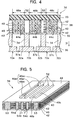
- Fig. 3 is an exploded perspective view showing an array 30 used in the ink jet print head 15.
- the array 30 includes a base plate 33 made from a metal or a ceramic with a high modulus of elasticity, a layered piezoelectric element 38 produced according to the method of the present invention, a thin-film vibration plate 35, a channel main body 34, and an orifice plate 36 formed with orifices 37. These components of the array 30 are attached together in the configuration shown in Fig. 3. That is, the base plate 33 is secured on one side of the layered piezoelectric element 38 and the thin-film vibration plate 35 is disposed to the other side of the layered piezoelectric element 38.
- the layered piezoelectric element 38 is attached, via the thin-film vibration plate 35, to one side of the channel main body 34 and the orifice plate 36 is attached to the other side of the channel main body 34.
- the channel main body 34 and the orifice plate 36 are formed by injection molding of a resin material.
- the layered piezoelectric element 38 has formed therein a plurality of slit-shaped elongated holes 52 defining therebetween actuator portions 46a, 46b, and 46c.
- the channel main body 34 has formed therein ink channels 32a, 32b, and 32c extending in parallel with and at positions corresponding to the actuator portions 46a, 46b, and 46c.
- the ink channels 32a, 32b, and 32c are formed longer in the lengthwise direction and wider in the widthwise direction than corresponding actuator portions 46a, 46b, and 46c of the layered piezoelectric element 38.
- the array 30 of the present embodiment includes three ejection devices 70a, 70b, 70c, which include the actuator portions 46a, 46b, and 46c and the ink channels 32a, 32b, and 32c respectively.
- the actuator portions 46a, 46b, and 46c of the layered piezoelectric element 38 are positioned at cavities formed by the ink channels 32a, 32b, and 32c (which extend perpendicular to the sheet surface of Fig. 4) so that the layered piezoelectric element 38 serves as a piezoelectric actuator for the three ejection devices 70a, 70b, and 70c.
- the layered piezoelectric element 38 is a multi-layered body including: piezoelectric ceramic layers 40 having piezoelectric and electrostrictive properties; internal negative electrode layers 42; and internal positive electrode layers 44a, 44b, and 44c.
- the piezoelectric ceramic layers 40 are composed of a lead zirconium titanate (PZT) ceramic material with ferroelectric properties. As indicated by arrows at the actuator portions 46a, 46b, and 46c in Fig. 4, the piezoelectric ceramic layers 40 are polarized in the direction in which they are layered.
- the internal negative electrode layers 42 and internal positive electrode layers 44a, 44b, and 44c are composed of a silver-palladium (Ag-Pd) metal material.
- the actuator portions 46a, 46b, and 46c are formed at the central portion of the layered piezoelectric element 38 and are divided by the plurality of elongated holes 52.
- the layered piezoelectric element 38 includes a piezoelectric inactive portion 48 at an edge portion thereof.
- the piezoelectric inactive portion 48 connects end portions of the actuator portions 46a, 46b, and 46c together.
- the internal positive electrode layers 44a, 44b, and 44c are divided by the elongated holes 52 to a one-to-one correspondence with the ink channels 32a, 32b, and 32c.
- the internal electrode layers 42, and 44a, 44b, and 44c overlap at overlapping regions 46a 1 (indicated by dotted lines in Fig. 5), 46b 1 , and 46c 1 , that is, at all areas between the elongated holes except the tips of each actuator portion 46a, 46b, and 46c.
- internal electrode layers 42, and 44a, 44b, and 44c do not overlap at the piezoelectric inactive portion 48 nor at non-overlapping regions 46a 2 (indicated by dotted lines in Fig. 5), 46b 2 , and 46c 2 , that is, at the tips of each actuator portion 46a, 46b, and 46c.
- the layered piezoelectric element 38 is produced using the following method.
- a piezoelectric material which is primarily PZT, is mixed in a desired composition.
- the powder is calcined at 850°C.
- a binder and other additives are added to the powder.
- the mixture dispersed in an organic solvent is mixed in a ball mill for 24 hours to form a piezoelectric material paste.
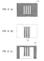
- screen print plates with patterns 100, 101, and 102 shown in Figs. 6 (a), 6 (b), and 6 (c) respectively are prepared.
- a metal die 110 shown in cross section in Figs. 7 (a) through 7 (c) is prepared with the same outward form as the pattern 100.
- the die 110 is recessed at portions thereof other than areas corresponding to the elongated holes 52.
- the metal die 110 and the screen print plate having a pattern with elongated hole portions formed to a predetermined pitch as shown in Fig. 6 (a) are positioned into alignment as shown in Fig. 7 (a). Then, a sheet of PET film is applied to the metal die 110 to prevent the piezoelectric material paste from sticking.
- the piezoelectric material paste is screen printed and dried to form an approximately 40 ⁇ m thick piezoelectric ceramic layer 40 as shown in Fig. 7 (b).
- the central portion of the piezoelectric ceramic layer 40 is divided into a plurality of actuator portions 46 by elongated hole portions 52.
- the metal die 110 is lowered a distance equal to the thickness of the printed piezoelectric material film.
- silver or palladium paste for forming the internal electrodes is screen printed to several microns' thickness on the piezoelectric material film using a screen print plate with the pattern 101 shown in Fig. 6 (b).
- the resultant green sheet will appear as shown in Fig. 8 (b).
- internal positive electrode layers 44a through 44c which are divided into a plurality having a one-to-one correspondence with the actuator portions, and electrode terminal portions 45a, 45b, and 45c are formed on the upper surface of the piezoelectric ceramic layer 40.
- piezoelectric material paste is printed using the screen print plate having the pattern 101 shown in Fig. 6 (a) and dried, resulting in the layered body shown in Fig. 8 (c).
- the internal electrode paste is printed using the screen print plate with the pattern 102 shown in Fig. 6 (c) and dried, resulting in the formation of an internal negative electrode layer 42, which traverses all the ink channels 32a through 32c, and its electrode terminal portions 43 as shown in Fig. 8 (d).
- a piezoelectric ceramic layer 40 is again printed and dried. Afterward, heat pressing is performed. Degreasing is performed at 500°C and sintering is performed at 1,200°C to obtain a layered body made from piezoelectric ceramics wherein piezoelectric ceramic layers 40 and internal electrodes 42 and 44 are alternately layered. The electrode terminal portions 43 and 54 of the internal electrodes 42 and 44 are exposed at one side surface.
- the piezoelectric ceramic layer 40 need not be limited to the approximately 40 micron thickness described in the present embodiment.
- the piezoelectric ceramic layer 40 can be formed using screen printing to the same several microns' thickness of the internal electrodes 42 and 44. Alternatively, when it is desired to form a thick piezoelectric ceramic layer 40, screen printing with the piezoelectric material paste can be repeated a plurality of times to form a layer with a desired thickness.
- Outer negative electrodes 53 and outer positive electrodes 54a, 54b, 54c are attached to locations where the electrode terminal portions 43, 45a, 45b, and 45c are exposed in the thus-formed layered body
- a well-known polarization process is executed to polarize the layered body by application of an electric field.
- the polarization process can be carried out, for example, by immersing the layered body into an oil bath (not shown) filled with an electrically insulating oil, such as silicon oil, heated to about 130°C.
- An electric field of approximately 2.5 kV/mm is then applied between the outer negative electrodes 53 and the outer positive electrodes 54a, 54b, and 54c to polarize the layered body.
- the piezoelectric ceramic layers 40 of the layered body are sufficiently thin, for example, approximately 50 ⁇ m, they can be easily polarized without providing a special environment such as the oil bath.
- a voltage of approximately 30 V is applied between the outer negative electrodes 53 and the outer positive electrodes 54a, 54b, and 54c after the ink jet print head 15 has been assembled.
- the layered piezoelectric element 38 shown in Fig. 5 can be obtained using the above method.
- the layered piezoelectric element 38 is mounted to an ink jet print head after polishing and shot blast processes.
- the layered piezoelectric element 38 formed through the above-described method has actuator portions 46a, 46b, and 46c connected by their end portions to the piezoelectric non-active region 48. Therefore, even if the actuator portions 46a, 46b, and 46c are thin, they will be supported by the piezoelectric non-active region 48 and so will not break or be damaged during production.
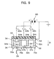
- Electric circuits provided in the array 30 are shown in Fig. 9.
- the outer positive electrodes 54a, 54b, and 54c of the layered piezoelectric element 38 are connected to the positive electrode of a drive power source 60 through openable and closable switches 62a, 62b, 62c.
- the outer negative electrodes 53 of the layered piezoelectric element 38 and the negative electrode of the drive power source 60 are grounded.
- a controller (not shown) opens and closes the switches 62a, 62b, and 62c to selectively apply a driving voltage from the drive power source 60 between the internal negative electrode layers 42 and the internal positive electrode layers 44 located on a selected one of the actuator portions 46a, 46b, or 46c.
- the controller closes, for example, the switch 62a so that a voltage is applied between the internal negative electrode layers 42 and internal positive electrode layers 44a of the actuator portion 46a, resulting in a bias electric field developing in the piezoelectric ceramic layers 40 between these internal electrode layers.
- Dimensional distortion caused by piezoelectric and electrostrictive longitudinal-effects lengthen the actuator portion 46a in the vertical direction of Fig. 9, thereby reducing the volume in the ink channel 32a.
- An increase in pressure accompanying this volume change ejects ink in the ink channel 32a from the orifice 37a as a droplet 39.
- the switch 62a is opened and the application of voltage is cut off, returning the actuator portion to its original form.
- ink is refilled into the ink channel 32a from the ink supply device 16 via a separate valve (not shown).
- a separate valve not shown
- displacement of the actuator portion 46b will occur so that ink will be ejected from the ink channel 32b.
- the piezoelectric ceramic layers 40 are polarized in the direction in which they are layered, a large amount of deformation develops in the layered direction, resulting in highly reliable ink ejection.
- the piezoelectric ceramic layer 40 can be made sufficiently thin using screen printing to allow ejection using a low drive voltage.
- Manufacturing a layered piezoelectric element according the method of the present invention eliminates the need to align plates when layering the plates. Also, there are no processes for removing, drying, stacking, and pressing the sheets. The method includes only repeating simple screen printing processes. Therefore, the method is easy to automate and production management can be simplified.
- the shape to which layers are formed can be freely set.
- a layered body can therefore be easily formed, without mechanical processes, in many shapes in accordance with the pattern shape of the screen print plate.
- print heads can be made in more compact sizes by forming piezoelectric elements in shapes that suit the shape of the print head. Mechanical processes are particularly minimized after sintering, which allows reductions in manufacturing costs.
- a piezoelectric element divided into a plurality of actuator portions can be prepared without performing any mechanical processes such as dicing.
- Screen printing allows forming thin layers, which allows providing a piezoelectric element that can be driven with a low voltage and allows producing a compact print head that uses the piezoelectric element.
- a single layered piezoelectric element 38 serves as piezoelectric actuators for all the ejection devices 70a, 70b, and 70c. Therefore, a plurality of arrays 30 assembled together can provide an ink jet print head 15 with a simple configuration that can be produced using simple methods. Therefore, the number and complexity of manufacturing processes can be reduced so that production costs can be reduced.
- the piezoelectric actuators are layered piezoelectric elements 38 and because the ink channels 32a, 32b, and 32c are formed longer in the lengthwise direction than corresponding actuator portions 46a, 46b, and 46c, consequently, the actuator portions 46a, 46b, and 46c can effectively and easily deform into corresponding ink channels 32a, 32b, and 32c so that driving voltage can be significantly reduced.
- the internal electrode layers 42, 44 of the layered piezoelectric element 38 are formed by screen printing, the electrodes can be simply formed even when the actuator portions 46a, 46b, and 46c and the elongated holes 52 are formed extremely thin. Therefore, an array 30 including the ejection devices 70a, 70b, and 70c can be formed to a small size so that a print head that allows high resolution and a wide printing range can be achieved.
- each of the actuator portions 46a, 46b, and 46c divided by the elongated holes 52 are supported connected together at their end portions by the piezoelectric non-active region 48. Consequently, even when the actuator portions 46a, 46b, and 46c are formed to a narrow width, they will not break or be damaged during production or drive of the print head. Therefore, yield when producing the print head is improved. The actuator portions 46a, 46b, and 46c will also not break when driven, thereby improving reliability of the resultant print head. Also, if the actuator portions 46a, 46b, and 46c can be formed thinner, they can be formed into a more highly integrated unit, which improves print quality of the resultant ink jet print head.
- the electrode terminal portions 43, 45 of the internal negative electrode layers 42 and internal positive electrode layers 44 of the layered piezo-electric element 38 according to the present embodiment are exposed to the exterior. Therefore, deterioration of insulating properties, such as deterioration caused by silver migration, is eliminated. Further, advantages such as superior durability and moisture resistance are gained. Also, because the outer negative electrodes 53 and the outer positive electrodes 54a, 54b, and 54c connected to the internal electrode layers 42, 44a, 44b, and 44c are formed on the same side surface of the layered piezoelectric element 38, the electrodes can be easily picked up and collectively electrically connected to a drive control circuit or a circuit substrate for controlling drive of the print head. Also, the outer negative electrodes 53 and the outer positive electrodes 54a, 54b, and 54c can be connected to the electric circuit at a single side surface of the array 30 so that less space is taken up.
- one layered piezoelectric element 38 serves as piezoelectric actuators for the three ejection devices 70a, 70b, and 70c.
- piezoelectric actuators for additional ejection devices can be formed by adding to, or changing the pattern of, the internal positive electrode layers 44.
- the internal positive electrode layers 44 are divided in a one-to-one correspondence to the ink channels 32a, 32b, and 32c.
- the internal negative electrode layers 42 may be divided to a one-to-one correspondence to the ink channels 32a, 32b, and 32c.
- both the internal positive electrode layers 44 and the internal negative electrode layers 42 may be separated in a one-to-one correspondence to the ink channels 32a, 32b, and 32c. That is, it is sufficient for at least one of the internal electrode layers, either positive or negative, to be divided in a one-to-one correspondence to the ink channels 32a, 32b, and 32c.
- the array 30 can be provided with more or less than the three ink channels described in the present embodiment.
- the electrode terminal portions 43 and 45 of the electrode layers 42 and 44 are exposed at the same single surface of the layered piezoelectric element 38.
- the electrode terminal portions 43 and 45 for the internal positive electrode layers 44 and the internal negative electrode layers 42 can be exposed from different side surfaces.
Claims (10)
- Méthode de production d'un élément piézoélectrique en couches destiné à provoquer une variation de pression dans une cavité d'une tête d'impression à jet d'encre pour éjecter l'encre de l'intérieur de la cavité, la méthode de production comportant les étapes suivantes :sérigraphier une suspension de matériau piézoélectrique en poudre pour former une couche en céramique piézoélectrique; etsérigraphier une pâte conductrice pour former une couche d'électrodes internes sur la couche en céramique piézoélectrique.
- Méthode de production d'un élément piézoélectrique en couches conformément à la revendication 1 comportant en outre une étape de répétition en alternance des étapes de sérigraphie de la suspension de matériau piézoélectrique en poudre et celles de sérigraphie de la pâte conductrice pour obtenir un corps en couches composé en alternance de couches en céramique piézoélectrique et de couches d'électrodes internes.
- Méthode de production d'un élément piézoélectrique en couches conformément à la revendication 2:dans laquelle on utilise, pour chaque autre réalisation de l'étape de sérigraphie de la pâte conductrice, une plaque de sérigraphie ayant une première forme permettant de former une première couche d'électrodes sur une couche en céramique piézoélectrique; etdans laquelle on utilise, pour la réalisation des étapes restantes de sérigraphie de la pâte conductrice, une plaque de sérigraphie ayant une seconde forme permettant de former une seconde couche d'électrodes sur une couche en céramique piézoélectrique qui est disposée sur une première couche d'électrodes.
- Méthode de production d'un élément piézoélectrique en couches conformément à la revendication 3 dans laquelle on utilise, lors de l'étape de sérigraphie de la suspension de matériau piézoélectrique en poudre, une plaque de sérigraphie ayant une forme faite de tronçons de trous indépendants oblongs pour former une couche en céramique piézoélectrique avec des trous définissant une pluralité de parties de l'actionneur sur au moins une partie centrale de la couche en céramique piézoélectrique.
- Méthode de production d'un élément piézoélectrique en couches conformément à la revendication 4:
dans laquelle chaque autre réalisation de l'étape de sérigraphie de la pâte conductrice forme la première couche d'électrodes en tant qu'électrode commune à toutes les parties de l'actionneur et dans laquelle les réalisations restantes de l'étape de sérigraphie de la pâte conductrice forment la seconde couche d'électrodes comme une pluralité d'électrodes d'entraínement indépendantes à des emplacements correspondants aux actionneurs de telle sorte que la première et la seconde couche d'électrodes sont juxtaposées en opposition au moins sur les parties séparées de l'actionneur dans un sens où le corps en couches est disposé. - Méthode de production d'un élément piézoélectrique en couches conformément à l'une quelconque des revendications 2 à 5 dans laquelle l'étape de sérigraphie d'une pâte conductrice forme une couche d'électrodes avec des tronçons à bornes sur un seul bord d'une couche en céramique piézoélectrique correspondante sur laquelle la couche d'électrodes est formée.
- Méthode de production d'un élément piézoélectrique en couches conformément à l'une quelconque des revendications 2 à 6 dans laquelle le fait de répéter l'étape de sérigraphie d'une pâte conductrice en alternance avec l'étape de sérigraphie d'une suspension de matériau piézoélectrique en poudre produit le corps en couches avec les tronçons à bornes des couches d'électrodes exposées d'un seul côté du corps en couches.
- Méthode de production d'un élément piézoélectrique en couches conformément à l'une quelconque des revendications 2 à 7, comportant en outre l'étape de polarisation des couches en céramique piézoélectrique dans un sens où un champ électrique est généré entre les couches d'électrodes quand on leur applique une tension.
- Méthode de production d'un élément piézoélectrique en couches conformément à la revendication 2:dans laquelle l'étape de sérigraphie de la suspension de matériau piézoélectrique en poudre comprend la sérigraphie de la suspension dans un moule en forme de feuille en utilisant une plaque de sérigraphie ayant une forme avec au moins une pluralité de régions indépendantes;dans laquelle l'étape de sérigraphie de la pâte conductrice comprend un premier processus utilisant une plaque de sérigraphie ayant une première forme permettant de former une première couche d'électrodes sur la couche en céramique piézoélectrique et un second processus utilisant une plaque de sérigraphie ayant une seconde forme permettant de former une seconde couche d'électrodes disposée sur la première couche d'électrodes, le premier et le second processus étant effectués en alternance l'un avec l'autre et avec l'étape de sérigraphie de la suspension de matériau piézoélectrique en poudre, effectuée entretemps pour former un corps en couches dans lequel chaque couche d'électrodes est prise en sandwich par des couches en céramique piézoélectrique et dans lequel les premières et les secondes couches d'électrodes alternent les unes avec les autres.
- Méthode de production d'un élément piézoélectrique en couches conformément à la revendication 9:
dans laquelle l'étape de sérigraphie de la suspension de matériau piézoélectrique en poudre utilise une plaque de sérigraphie ayant une forme faite de tronçons de trous indépendants oblongs ayant un espacement prédéterminé pour former une couche en céramique piézoélectrique divisée en une pluralité de parties de l'actionneur sur au moins une partie centrale de la couche en céramique piézoélectrique;dans laquelle le premier processus forme la première couche d'électrodes en tant qu'électrode commune à toutes les parties de l'actionneur; etdans laquelle le second processus forme la seconde couche d'électrodes comme une pluralité d'électrodes d'entraínement indépendantes correspondant aux actionneurs; etdans laquelle la première et la seconde couche d'électrodes sont juxtaposées en opposition au moins sur les parties divisées de l'actionneur dans un sens où le corps en couches est disposé.
Applications Claiming Priority (3)
| Application Number | Priority Date | Filing Date | Title |
|---|---|---|---|
| JP57019/95 | 1995-03-16 | ||
| JP5701995A JPH08252920A (ja) | 1995-03-16 | 1995-03-16 | 積層型圧電素子の製造方法 |
| JP5701995 | 1995-03-16 |
Publications (3)
| Publication Number | Publication Date |
|---|---|
| EP0732209A2 EP0732209A2 (fr) | 1996-09-18 |
| EP0732209A3 EP0732209A3 (fr) | 1998-01-07 |
| EP0732209B1 true EP0732209B1 (fr) | 2000-06-07 |
Family
ID=13043732
Family Applications (1)
| Application Number | Title | Priority Date | Filing Date |
|---|---|---|---|
| EP96301786A Expired - Lifetime EP0732209B1 (fr) | 1995-03-16 | 1996-03-15 | Méthode de production d'un élément piézoélectrique en couches |
Country Status (4)
| Country | Link |
|---|---|
| US (1) | US5639508A (fr) |
| EP (1) | EP0732209B1 (fr) |
| JP (1) | JPH08252920A (fr) |
| DE (1) | DE69608722T2 (fr) |
Families Citing this family (38)
| Publication number | Priority date | Publication date | Assignee | Title |
|---|---|---|---|---|
| JPH08187848A (ja) * | 1995-01-12 | 1996-07-23 | Brother Ind Ltd | 積層式圧電素子およびその製造方法 |
| JP3663652B2 (ja) * | 1995-02-13 | 2005-06-22 | ブラザー工業株式会社 | インクジェットプリンタヘッド |
| JP3267171B2 (ja) * | 1996-09-12 | 2002-03-18 | 株式会社村田製作所 | 圧電共振子およびそれを用いた電子部品 |
| JP3365224B2 (ja) * | 1996-10-24 | 2003-01-08 | セイコーエプソン株式会社 | インクジェット式記録ヘッドの製造方法 |
| KR100209515B1 (ko) * | 1997-02-05 | 1999-07-15 | 윤종용 | 자성잉크를 이용한 잉크젯 프린터의 분사 장치 및 방법 |
| JP3271540B2 (ja) * | 1997-02-06 | 2002-04-02 | ミノルタ株式会社 | インクジェット記録装置 |
| US6053602A (en) * | 1997-02-28 | 2000-04-25 | Hitachi Koki Company Ltd. | On-demand multi-nozzle ink jet head |
| JP3575239B2 (ja) * | 1997-08-05 | 2004-10-13 | ブラザー工業株式会社 | インクジェットヘッド及びその製造方法 |
| EP0908961B1 (fr) * | 1997-10-13 | 2003-06-04 | Sagem S.A. | Actionneur amplifié à matériaux actifs |
| US6291932B1 (en) * | 1998-02-17 | 2001-09-18 | Canon Kabushiki Kaisha | Stacked piezoelectric element and producing method therefor |
| JP3849145B2 (ja) * | 1998-02-18 | 2006-11-22 | ソニー株式会社 | 圧電アクチユエータの製造方法 |
| JP3780700B2 (ja) * | 1998-05-26 | 2006-05-31 | セイコーエプソン株式会社 | パターン形成方法、パターン形成装置、パターン形成用版、パターン形成用版の製造方法、カラーフィルタの製造方法、導電膜の製造方法及び液晶パネルの製造方法 |
| US6367132B2 (en) * | 1998-08-31 | 2002-04-09 | Eastman Kodak Company | Method of making a print head |
| US6572830B1 (en) | 1998-10-09 | 2003-06-03 | Motorola, Inc. | Integrated multilayered microfludic devices and methods for making the same |
| US6592696B1 (en) | 1998-10-09 | 2003-07-15 | Motorola, Inc. | Method for fabricating a multilayered structure and the structures formed by the method |
| DE19850610A1 (de) * | 1998-11-03 | 2000-05-04 | Bosch Gmbh Robert | Verfahren zur Herstellung piezoelektrischer Aktoren |
| JP4240245B2 (ja) * | 1998-12-15 | 2009-03-18 | 富士フイルム株式会社 | インクジェットプリンタヘッド及びインクジェットプリンタ |
| JP2000270574A (ja) * | 1999-03-16 | 2000-09-29 | Seiko Instruments Inc | 圧電アクチュエータおよびその製造方法 |
| US6447887B1 (en) | 1999-09-14 | 2002-09-10 | Virginia Tech Intellectual Properties, Inc. | Electrostrictive and piezoelectric thin film assemblies and method of fabrication therefor |
| JP3716724B2 (ja) * | 1999-09-30 | 2005-11-16 | ブラザー工業株式会社 | 圧電式インクジェットプリンタヘッドの圧電アクチュエータ及びその製造方法 |
| JP3956607B2 (ja) * | 2000-10-26 | 2007-08-08 | ブラザー工業株式会社 | 圧電式インクジェットプリンタヘッド及び圧電式インクジェットプリンタヘッドの製造方法 |
| JP4042442B2 (ja) * | 2001-03-29 | 2008-02-06 | ブラザー工業株式会社 | 圧電トランスデューサおよび液滴噴射装置 |
| JP4296738B2 (ja) * | 2001-11-30 | 2009-07-15 | ブラザー工業株式会社 | インクジェットヘッド |
| JP4059116B2 (ja) * | 2003-03-20 | 2008-03-12 | ブラザー工業株式会社 | インクジェットヘッド及びその製造方法 |
| JP4842520B2 (ja) * | 2003-05-30 | 2011-12-21 | 日本碍子株式会社 | セル駆動型圧電/電歪アクチュエータ及びその製造方法 |
| JP2005014506A (ja) * | 2003-06-27 | 2005-01-20 | Ricoh Printing Systems Ltd | インクジェットヘッド及びインクジェット式記録装置 |
| US7201473B2 (en) * | 2003-06-30 | 2007-04-10 | Brother Kogyo Kabushiki Kaisha | Inkjet printing head |
| JP4525094B2 (ja) * | 2004-01-30 | 2010-08-18 | ブラザー工業株式会社 | インクジェットヘッドの製造方法 |
| JP5512065B2 (ja) * | 2005-02-08 | 2014-06-04 | Tdk株式会社 | 圧電セラミック素子 |
| US20070093698A1 (en) * | 2005-10-20 | 2007-04-26 | Glucon Inc. | Apparatus and methods for attaching a device to a body |
| US20070093717A1 (en) * | 2005-10-20 | 2007-04-26 | Glucon Inc. | Wearable glucometer configurations |
| US8113635B2 (en) * | 2007-01-16 | 2012-02-14 | Brother Kogyo Kabushiki Kaisha | Liquid discharge apparatus and check method of the same |
| JP5181914B2 (ja) * | 2008-08-08 | 2013-04-10 | ブラザー工業株式会社 | 位置決め方法 |
| US8813324B2 (en) | 2010-03-24 | 2014-08-26 | Western Digital (Fremont), Llc | Method for providing a piezoelectric multilayer |
| DE102011003680A1 (de) | 2011-02-07 | 2012-08-09 | Robert Bosch Gmbh | Verfahren zur Herstellung von piezoelektrischen Werkstücken |
| KR101328345B1 (ko) * | 2011-08-29 | 2013-11-11 | 삼성전기주식회사 | 압전체 조성물, 압전 소자, 잉크젯 프린트 헤드 및 압전 소자와 잉크젯 프린터 헤드의 제조방법 |
| KR101537939B1 (ko) * | 2013-12-04 | 2015-07-20 | 한국세라믹기술원 | 압전 세라믹 파이버 적층형 복합소자 및 그 제조방법 |
| US10680161B1 (en) | 2017-03-29 | 2020-06-09 | Apple Inc. | Electronic Devices with Piezoelectric Ink |
Family Cites Families (12)
| Publication number | Priority date | Publication date | Assignee | Title |
|---|---|---|---|---|
| EP0094078B1 (fr) * | 1982-05-11 | 1988-11-02 | Nec Corporation | Elément électrostrictif multicouche résistant à l'application répétée d'impulsions |
| JPS6127688A (ja) * | 1984-07-02 | 1986-02-07 | Nec Corp | 電歪効果素子およびその製造方法 |
| JPS62133777A (ja) * | 1985-12-05 | 1987-06-16 | Hitachi Metals Ltd | 積層型圧電素子およびその製造方法 |
| EP0427901B1 (fr) * | 1989-11-14 | 1996-04-03 | Battelle Memorial Institute | Procédé de fabrication d'un actionneur à couches piézoélectriques empilées |
| JP3041952B2 (ja) * | 1990-02-23 | 2000-05-15 | セイコーエプソン株式会社 | インクジェット式記録ヘッド、圧電振動体、及びこれらの製造方法 |
| US5402159A (en) * | 1990-03-26 | 1995-03-28 | Brother Kogyo Kabushiki Kaisha | Piezoelectric ink jet printer using laminated piezoelectric actuator |
| JP2913806B2 (ja) * | 1990-09-14 | 1999-06-28 | ブラザー工業株式会社 | 圧電式インクジェットプリンタヘッド |
| JP3045531B2 (ja) * | 1990-10-01 | 2000-05-29 | 日立金属株式会社 | 積層型変位素子 |
| JP2836332B2 (ja) * | 1991-12-20 | 1998-12-14 | 日本電気株式会社 | 積層圧電アクチュエータ素子の製造方法 |
| JP3257151B2 (ja) * | 1993-06-18 | 2002-02-18 | 東ソー株式会社 | 熱可塑性エラストマー組成物及びその製造法 |
| JPH0757545B2 (ja) * | 1993-07-19 | 1995-06-21 | セイコーエプソン株式会社 | インクジェットヘッド及びその製造方法 |
| JP3088890B2 (ja) * | 1994-02-04 | 2000-09-18 | 日本碍子株式会社 | 圧電/電歪膜型アクチュエータ |
-
1995
- 1995-03-16 JP JP5701995A patent/JPH08252920A/ja active Pending
-
1996
- 1996-03-11 US US08/613,662 patent/US5639508A/en not_active Expired - Lifetime
- 1996-03-15 EP EP96301786A patent/EP0732209B1/fr not_active Expired - Lifetime
- 1996-03-15 DE DE69608722T patent/DE69608722T2/de not_active Expired - Lifetime
Also Published As
| Publication number | Publication date |
|---|---|
| EP0732209A2 (fr) | 1996-09-18 |
| DE69608722D1 (de) | 2000-07-13 |
| JPH08252920A (ja) | 1996-10-01 |
| EP0732209A3 (fr) | 1998-01-07 |
| US5639508A (en) | 1997-06-17 |
| DE69608722T2 (de) | 2000-10-05 |
Similar Documents
| Publication | Publication Date | Title |
|---|---|---|
| EP0732209B1 (fr) | Méthode de production d'un élément piézoélectrique en couches | |
| EP0721839B1 (fr) | Elément piézoélectrique à couches et méthode de production de cet élément | |
| US5860202A (en) | Method for producing a layered piezoelectric element | |
| JP2913806B2 (ja) | 圧電式インクジェットプリンタヘッド | |
| US6575565B1 (en) | Piezo-electric actuator of ink jet printer head and method for producing same | |
| US5128694A (en) | Head for ink-jet printer | |
| US6863383B2 (en) | Piezoelectric transducer and ink ejector using the piezoelectric transducer | |
| JP3249545B2 (ja) | 圧電式インクジェットプリンタヘッド | |
| US20040155944A1 (en) | Piezoelectric ink jet print head and method of making the same | |
| US6109738A (en) | Ink jet print head and a method of manufacturing the same | |
| US6739704B2 (en) | Piezoelectric transducer and ink ejector using piezoelectric transducer | |
| EP1705012A2 (fr) | Actuateur piézo-électrique, dispositif de transport de liquide et méthode de production d'actuateur piézo-électrique | |
| US5945773A (en) | Piezoelectric actuator for ink-jet printer and method of manufacturing the same | |
| JP3128857B2 (ja) | 圧電式インクジェットプリンタヘッド | |
| EP1456034B1 (fr) | Module d'impression par jet d'encre a faible tension | |
| JPH0349957A (ja) | 圧電式インクジェットプリンタヘッド | |
| JPH06312505A (ja) | 積層型圧電変位素子及びそれを用いたインクジェット記録ヘッド | |
| JP3997729B2 (ja) | 圧電アクチュエータ及びその圧電アクチュエータを用いたインクジェットヘッド並びにそれらの製造方法 | |
| JP2002225269A (ja) | インクジェットプリンタヘッドおよびその圧電素子 | |
| JPH03274159A (ja) | 圧電式インクジェットプリンタヘッド | |
| JP3156411B2 (ja) | インクジェット式印字ヘッド及びその製造方法 | |
| JP3385692B2 (ja) | インクジェット用圧電体母部材及びそれを用いたインクジェットヘッド用圧電変位素子 | |
| JP3365510B2 (ja) | インクジェット式記録ヘッドの製造方法 | |
| JPH04235041A (ja) | インクジェット式印字ヘッド | |
| JP3266893B2 (ja) | 圧電式インクジェットプリンタヘッド |
Legal Events
| Date | Code | Title | Description |
|---|---|---|---|
| PUAI | Public reference made under article 153(3) epc to a published international application that has entered the european phase |
Free format text: ORIGINAL CODE: 0009012 |
|
| AK | Designated contracting states |
Kind code of ref document: A2 Designated state(s): DE GB |
|
| PUAL | Search report despatched |
Free format text: ORIGINAL CODE: 0009013 |
|
| AK | Designated contracting states |
Kind code of ref document: A3 Designated state(s): DE GB |
|
| 17P | Request for examination filed |
Effective date: 19980608 |
|
| GRAG | Despatch of communication of intention to grant |
Free format text: ORIGINAL CODE: EPIDOS AGRA |
|
| 17Q | First examination report despatched |
Effective date: 19990917 |
|
| GRAG | Despatch of communication of intention to grant |
Free format text: ORIGINAL CODE: EPIDOS AGRA |
|
| GRAH | Despatch of communication of intention to grant a patent |
Free format text: ORIGINAL CODE: EPIDOS IGRA |
|
| GRAH | Despatch of communication of intention to grant a patent |
Free format text: ORIGINAL CODE: EPIDOS IGRA |
|
| GRAA | (expected) grant |
Free format text: ORIGINAL CODE: 0009210 |
|
| AK | Designated contracting states |
Kind code of ref document: B1 Designated state(s): DE GB |
|
| REF | Corresponds to: |
Ref document number: 69608722 Country of ref document: DE Date of ref document: 20000713 |
|
| EN | Fr: translation not filed | ||
| PLBE | No opposition filed within time limit |
Free format text: ORIGINAL CODE: 0009261 |
|
| STAA | Information on the status of an ep patent application or granted ep patent |
Free format text: STATUS: NO OPPOSITION FILED WITHIN TIME LIMIT |
|
| 26N | No opposition filed | ||
| REG | Reference to a national code |
Ref country code: GB Ref legal event code: IF02 |
|
| PGFP | Annual fee paid to national office [announced via postgrant information from national office to epo] |
Ref country code: GB Payment date: 20150224 Year of fee payment: 20 |
|
| PGFP | Annual fee paid to national office [announced via postgrant information from national office to epo] |
Ref country code: DE Payment date: 20150331 Year of fee payment: 20 |
|
| REG | Reference to a national code |
Ref country code: DE Ref legal event code: R071 Ref document number: 69608722 Country of ref document: DE |
|
| REG | Reference to a national code |
Ref country code: GB Ref legal event code: PE20 Expiry date: 20160314 |
|
| PG25 | Lapsed in a contracting state [announced via postgrant information from national office to epo] |
Ref country code: GB Free format text: LAPSE BECAUSE OF EXPIRATION OF PROTECTION Effective date: 20160314 |