EP0730256A1 - Steuerverfahren einer Anzeige mit Parallelsteuerung von Pixelgruppen und Struktur dieser Anzeige - Google Patents
Steuerverfahren einer Anzeige mit Parallelsteuerung von Pixelgruppen und Struktur dieser Anzeige Download PDFInfo
- Publication number
- EP0730256A1 EP0730256A1 EP96103048A EP96103048A EP0730256A1 EP 0730256 A1 EP0730256 A1 EP 0730256A1 EP 96103048 A EP96103048 A EP 96103048A EP 96103048 A EP96103048 A EP 96103048A EP 0730256 A1 EP0730256 A1 EP 0730256A1
- Authority
- EP
- European Patent Office
- Prior art keywords
- group
- time
- groups
- display
- illuminated
- Prior art date
- Legal status (The legal status is an assumption and is not a legal conclusion. Google has not performed a legal analysis and makes no representation as to the accuracy of the status listed.)
- Withdrawn
Links
Images

Classifications
-
- G—PHYSICS
- G09—EDUCATION; CRYPTOGRAPHY; DISPLAY; ADVERTISING; SEALS
- G09G—ARRANGEMENTS OR CIRCUITS FOR CONTROL OF INDICATING DEVICES USING STATIC MEANS TO PRESENT VARIABLE INFORMATION
- G09G3/00—Control arrangements or circuits, of interest only in connection with visual indicators other than cathode-ray tubes
- G09G3/20—Control arrangements or circuits, of interest only in connection with visual indicators other than cathode-ray tubes for presentation of an assembly of a number of characters, e.g. a page, by composing the assembly by combination of individual elements arranged in a matrix no fixed position being assigned to or needed to be assigned to the individual characters or partial characters
- G09G3/22—Control arrangements or circuits, of interest only in connection with visual indicators other than cathode-ray tubes for presentation of an assembly of a number of characters, e.g. a page, by composing the assembly by combination of individual elements arranged in a matrix no fixed position being assigned to or needed to be assigned to the individual characters or partial characters using controlled light sources
-
- G—PHYSICS
- G09—EDUCATION; CRYPTOGRAPHY; DISPLAY; ADVERTISING; SEALS
- G09G—ARRANGEMENTS OR CIRCUITS FOR CONTROL OF INDICATING DEVICES USING STATIC MEANS TO PRESENT VARIABLE INFORMATION
- G09G3/00—Control arrangements or circuits, of interest only in connection with visual indicators other than cathode-ray tubes
- G09G3/20—Control arrangements or circuits, of interest only in connection with visual indicators other than cathode-ray tubes for presentation of an assembly of a number of characters, e.g. a page, by composing the assembly by combination of individual elements arranged in a matrix no fixed position being assigned to or needed to be assigned to the individual characters or partial characters
- G09G3/22—Control arrangements or circuits, of interest only in connection with visual indicators other than cathode-ray tubes for presentation of an assembly of a number of characters, e.g. a page, by composing the assembly by combination of individual elements arranged in a matrix no fixed position being assigned to or needed to be assigned to the individual characters or partial characters using controlled light sources
- G09G3/30—Control arrangements or circuits, of interest only in connection with visual indicators other than cathode-ray tubes for presentation of an assembly of a number of characters, e.g. a page, by composing the assembly by combination of individual elements arranged in a matrix no fixed position being assigned to or needed to be assigned to the individual characters or partial characters using controlled light sources using electroluminescent panels
- G09G3/32—Control arrangements or circuits, of interest only in connection with visual indicators other than cathode-ray tubes for presentation of an assembly of a number of characters, e.g. a page, by composing the assembly by combination of individual elements arranged in a matrix no fixed position being assigned to or needed to be assigned to the individual characters or partial characters using controlled light sources using electroluminescent panels semiconductive, e.g. using light-emitting diodes [LED]
-
- G—PHYSICS
- G09—EDUCATION; CRYPTOGRAPHY; DISPLAY; ADVERTISING; SEALS
- G09G—ARRANGEMENTS OR CIRCUITS FOR CONTROL OF INDICATING DEVICES USING STATIC MEANS TO PRESENT VARIABLE INFORMATION
- G09G2230/00—Details of flat display driving waveforms
Definitions
- the present invention relates, in general, to display devices, and more particularly, to a novel control scheme for operating a display.
- Matrix addressing techniques are well known in the art and have been utilized to control various types of displays such as light emitting diode (LED) displays, and field emission device (FED) displays.
- Matrix addressing schemes typically organize the light emitting elements or pixels into a number of rows and columns with each pixel at an intersection of a particular row and a particular column. Illuminating the pixel requires activating an intersecting row and column thereby providing a closed current path that includes the pixel to be illuminated.
- each pixel must be driven with a larger current to provide a pixel intensity that maintains acceptable image intensity and viewing characteristics. Driving the pixel with a larger current generally results in reducing the useful lifetime of the pixel thereby limiting the useful lifetime of the display.
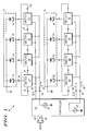
- FIG. 1 schematically illustrates a light emitting diode (LED) display 10.
- Display 10 includes a first plurality of LEDs including a first LED 12, a second LED 13, a third LED 14, and a fourth LED 16 that are organized together into a first group 11, illustrated by a dashed box.
- a second plurality of pixels includes a fifth LED 42, a sixth LED 43, a seventh LED 44, and an eighth LED 46 that are organized into a second group 41, illustrated by a dashed box.
- the cathode of LEDs 12, 13, 14, and 16 are each connected to ground, and an anode of LEDs 12, 13, 14, and 16 are connected to an output of a first switch 17, a second switch 18, a third switch 19, and a fourth switch 21, respectively.
- each switch and LED for example LED 12 and switch 17, form a pixel of display 10.
- Groups 11 and 41 generally are organized as the pixels within a single display line or row of a display, although groups 11 and 41 could be organized as a vertical display line or column of a display or any other organization of display elements of a display. Although only two groups are illustrated, a display can have any number of groups and any number of LEDs in a group.
- a controller 24 operates group 11 and group 41 in parallel and utilizes the entire frame time of display 10 for displaying the information for group 11 and also the entire frame time to display the information for group 41.
- the frame time is apportioned between the LEDs of group 11 that are to be illuminated, and LEDs that do not have data to be displayed are not illuminated.
- Each LED that is to be illuminated within group 11 is sequentially illuminated so that only one LED within group 11 is illuminated at a time, however, group 11 and 41 are operating in parallel so that more than one LED of display 10 can be illuminated simultaneously. Because the entire frame time is apportioned between the LEDs that are to be illuminated in group 11, the amount of time utilized to illuminate a particular LED is increased.
- Group 41 is operated in a similar manner in parallel with group 11.
- Controller 24 receives informational data 60, for example 8-bit parallel data, to be displayed by display 10, stores the data, partitions and decodes the data into individual pixel data, and uses the individual pixel data to operate groups 11 and 41.
- controller 24 develops a first enable signal (E1) 26 that is connected to an enable input of switches 17, 18, 19, and 21 in order to control or enable the illumination of LEDs 12, 13, 14, and 16.
- Controller 24 also has a first current control output 28 that is connected to a current input of switches 17, 18, 19, and 21 in order to supply a first variable drive current 29 to LEDs 12, 13, 14, and 16, respectively.
- Drive current 29 is developed as the output of a variable current source 22 that is a part of controller 24. Controller 24 controls the amount of drive current 29 supplied by source 22. Controller 24 also has a second variable current source 53 that functions similarly to source 22. Source 53 has a second current output 58 that provides a second variable drive current 59 for switches 47 48, 49, and 51 similarly to drive current 29.
- the length of time an LED within a group is illuminated is referred to as the active time for the group and the LEDs within the group.
- the active time for each group varies depending on the data to be displayed by the group.
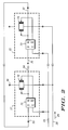
- FIG. 2 schematically illustrates an implementation suitable for switches 17, 18, 19, 21, 47, 48, 49, and 51 that are shown in FIG. 1. Elements of FIG. 2 that have the same reference numerals as FIG. 1 are the same as the corresponding FIG. 1 elements.
- Switches 17, 18, 19, and 21 (FIG. 1) have serial connections that facilitate forming a recirculating loop of a recirculating one in a field of zero's that is clocked from switch to switch by enable signal 26, and is utilized to sequentially enable each of LEDs 12, 13, 14, and 16 (FIG. 1). The technique of using a recirculating one in a field of zero's is well known to those skilled in the art.
- Each of switches 17, 18, 19, and 21 (FIG.
- switch 21 has a serial input 31 that is connected to a serial output of switch 19, and a serial output 32 that is connected to a serial input 33 of switch 17.
- Switch 17 has a serial output 34 that is connected to a serial input of switch 18.
- Switch 17 has a storage element that is used to provide the recirculating one in a field of zeros that is used to sequentially couple output 28 to LED 12.
- the storage element is a flip-flop 71 having a clock input connected to signal 26 and a shift input connected to input 33 of switch 17 so that output 32 of switch 21 may be shifted into switch 17.
- Outputs Q and of flip-flop 71 are connected to a transmission gate 72 in order to couple current 29 from output 28 to output 36 of switch 17 thereby applying current 29 to LED 12.
- switch 21 has a flip-flop 73 that functions similarly to flip-flop 71, and a transmission gate 74 that functions similarly to transmission gate 72.
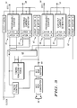
- FIG. 3 schematically illustrates a block diagram implementation that is suitable for controller 24 shown in FIG. 1. Elements of FIG. 3 that have the same reference numbers as FIG. 1 are the same elements as the corresponding FIG. 1 elements. Controller 24 can be implemented in a variety of ways.
- the block diagram shown in FIG 3 is an example of one implementation method.
- Data 60 is presented to controller 24 where a Bit Map Converter converts the data to a bit mapped representation of the image to be displayed, then stores the converted information in a Bit Map Buffer.
- Bit map converters and buffers are well known in the art.
- a timing and control section receives a clock signal and controls the bit map buffer to provide bit mapped data 64 for a particular group, e.g.
- Timing ROM/Look-up Table that generates a timing sequence that follows the equation given in FIG. 1 for the bit mapped information for the group.
- the timing sequence is stored, via a multiplexer 63, into a latch A of a sequencer or programmable counter 61, and into a latch A of variable current source 22.
- bit mapped data 64 for group 11 is stored in a group buffer A of a group buffer 62.
- Controller 24 uses two group buffers (buffer A and buffer B) and two latches (latch A and latch B) for each of counter 61 and source 22 to facilitate storing information for a subsequent frame while information for the current frame is being displayed.
- a Logic/Timing section receives the clock and an output of the Timing and Control section to facilitate controlling the operation of counter 61 and source 22 as shown in FIG. 4.
- bit map data 64 for group 41 is provided to group buffer A of a group buffer 67, and to the Timing ROM/Look-up Table then to a latch A of a programmable counter 66 and to a latch A of variable current source 53.
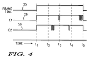
- FIG. 4 is a timing diagram illustrating an example of the operation of enable signals 26 and 56 that are shown in FIG. 1 and FIG. 3. Portions of FIG. 4 that have the same reference numerals as FIG. 1 are the same as the corresponding FIG. 1 elements.
- the abscissa of FIG. 4 represents time and is divided into four equal time slots indicated by time points t 1 , t 2 , t 3 , t 4 , and t 5 .
- Time points t 1- t 5 represent the points where LEDs would switch if all four LEDs in a group were to be illuminated.
- a frame time signal 25 is used as a reference to illustrate the time in which data is to be displayed by display 10 of FIG. 1.
- Frame time signal 25 becomes active at time t 1 when display 10 can display information.
- controller 24 utilizes the equation shown in the discussion of FIG. 1 to determine a first active time for group 11 and a separate second active time for group 41. Additionally, controller 24 sets output current 29 to a value that will provide a maximum illumination intensity or desired illumination intensity for LEDs 12 and 13 during the first active time, and sets output current 59 to a value that will provide the desired illumination intensity for LEDs 42, 44, and 46 during the second active time.
- the desired illumination intensity typically is equivalent to a maximum illumination intensity for the LED, that is, equivalent to the illumination intensity provided by the maximum current of the LED for a pixel time of a normal raster scan CRT display.
- the desired illumination intensity can be less in order to provide the lower intensity grey scale images. Because display 10 utilizes the entire frame time for each group 11 and 41, currents 29 and 59, respectively, are less than the maximum current of the LED, yet the desired intensity can equal the equivalent maximum LED intensity.
- enable signal 26 must have transitions to create a clock signal for the flip-flop storage elements of switches 19 and 21. These transitions are created by taking signal 26 low for a minimum clock time that is just sufficient for a clock set-up time for the flip-flop, and then taking signal 26 high for a minimum display time to create a transition that clocks data into the flip-flop. The minimum display time is just sufficient to clock data into the flip-flop. During this minimum display time, source 22 typically is disabled to prevent current 29 from creating an image during the minimum display time. Alternately, current 29 can be coupled to drive the corresponding LED, but since the time that signal 26 remains high is limited, the short time prevents creating an observable image on display 10 (FIG. 1).
- controller 24 calculates the first active time using the equation shown in the discussion of FIG. 1 to allocate the frame time among the two LEDs 12, and 13 and a minimum display time that is allocated to LEDs 14 and 16.
- Signal 26 (E 1 ) becomes active at time t 1 when signal 25 becomes active. Since the recirculating one is stored in switch 21, this causes switch 17 to clock the recirculating one on output 32 of switch 21 into switch 17 thereby enabling switch 17 to apply current 29 to LED 12.
- Signal 26 remains high for the first active time (past time point t 2 ), goes low for a minimum clock time then goes high prior to time t 3 to clock the recirculating one on output 34 of switch 17 into switch 18 thereby enabling switch 18 to apply current 29 to LED 13.
- Signal 26 remains high for the first active time so that LED 13 is illuminated for a time equal to the time LED 12 was illuminated, and then goes low for a minimum clock time, goes high for a minimum display time to clock the output of switch 18 into switch 19 thereby enabling LED 14 to apply current 29 to LED 14 for the minimum display time, goes low for a minimum clock time, and goes high for a minimum display time again to clock the output of switch 19 into switch 21 thereby disabling switch 19 and enabling switch 21 to apply current 29 to LED 16 for the minimum display time.
- signal 25 goes low to indicate the end of the frame time, thus, signal 26 goes low and controller 24 disables current source 22 thereby preventing the illumination of group 11.
- signal 56 (E 2 ) is used to illuminate LEDs 42, 44, and 46 of group 41.
- controller 24 calculates the second active time using the equation shown in the discussion of FIG. 1 to allocate the frame time among the three LEDs 42, 44, and 46 and a minimum display time that is allocated to LED 43.
- Signal 56 (E 2 ) becomes active at t 1 in parallel with signal 26 so that groups 11 and 41 are operating simultaneously.
- Signal 56 remains high for the second active time past t 2 but for a time less than the first active time because group 41 has three LEDs illuminated whereas group 11 only has two LEDs.
- Signal 56 then goes low for a minimum clock cycle and then back high for a minimum display time to clock the recirculating one from switch 47 into switch 48 thereby enabling LED 43 for the minimum display time, then back low for a minimum clock cycle and back high again to clock the recirculating one into switch 49 thereby enabling LED 44 for the second active time. While LED 43 is briefly enabled during the minimum display time, controller 24 can set current 59 to zero to prevent illuminating LED 43, or can leave current 59 unaffected since the time LED 43 is illuminated is so brief that an image will not be perceived by an individual observing display 10.
- Signal 56 remains high for the second active time for LED 44, and then goes low and back high again to clock the output of switch 49 into switch 51 thereby enabling switch 51 to apply current 59 to LED 46 for the second active time thereby illuminating LED 46 for the second active time. Thereafter, signal 25 goes low to indicate the end of the frame time, thus, signal 56 goes low and controller 24 (FIG. 1) disables current source 53 thereby preventing the illumination of group 41.
- FIG. 5 is a perspective view illustrating display 10 implemented as a monolithic semiconductor display on a semiconductor substrate 75. Elements of FIG. 5 that have the same reference numerals as FIG. 1 are the same as the corresponding FIG. 1 elements.
Landscapes
- Engineering & Computer Science (AREA)
- Physics & Mathematics (AREA)
- Computer Hardware Design (AREA)
- General Physics & Mathematics (AREA)
- Theoretical Computer Science (AREA)
- Control Of Indicators Other Than Cathode Ray Tubes (AREA)
- Control Of El Displays (AREA)
Applications Claiming Priority (2)
| Application Number | Priority Date | Filing Date | Title |
|---|---|---|---|
| US08/398,270 US5644328A (en) | 1995-03-03 | 1995-03-03 | Apparatus and method for operating groups of led display pixels in parallel to maximize active time |
| US398270 | 1999-09-17 |
Publications (1)
| Publication Number | Publication Date |
|---|---|
| EP0730256A1 true EP0730256A1 (de) | 1996-09-04 |
Family
ID=23574717
Family Applications (1)
| Application Number | Title | Priority Date | Filing Date |
|---|---|---|---|
| EP96103048A Withdrawn EP0730256A1 (de) | 1995-03-03 | 1996-02-29 | Steuerverfahren einer Anzeige mit Parallelsteuerung von Pixelgruppen und Struktur dieser Anzeige |
Country Status (6)
| Country | Link |
|---|---|
| US (1) | US5644328A (de) |
| EP (1) | EP0730256A1 (de) |
| JP (1) | JPH08263009A (de) |
| KR (1) | KR960035418A (de) |
| CN (1) | CN1135068A (de) |
| TW (1) | TW290676B (de) |
Families Citing this family (6)
| Publication number | Priority date | Publication date | Assignee | Title |
|---|---|---|---|---|
| US6894663B1 (en) | 1995-10-31 | 2005-05-17 | Mitchell A. Altman | Method for creating an image for an event or promotion |
| US6239774B1 (en) * | 1995-10-31 | 2001-05-29 | Mitchell A. Altman | Persistent image maker |
| KR100783707B1 (ko) * | 2001-10-18 | 2007-12-07 | 삼성전자주식회사 | 유기 전계발광 패널과 이를 포함하는 유기 전계발광 표시장치와 이의 구동 장치 및 구동 방법 |
| JP4577525B2 (ja) | 2007-05-31 | 2010-11-10 | 東芝ライテック株式会社 | 照明装置 |
| US8344632B2 (en) * | 2009-12-15 | 2013-01-01 | Silicon Touch Technology Inc. | Light emitting device |
| US9818337B2 (en) * | 2014-07-24 | 2017-11-14 | Sct Technology, Ltd. | LED display control circuit with PWM circuit for driving a plurality of LED channels |
Citations (4)
| Publication number | Priority date | Publication date | Assignee | Title |
|---|---|---|---|---|
| US3986186A (en) * | 1974-12-23 | 1976-10-12 | Hewlett-Packard Company | Automatic display segment intensity control |
| DE2756710A1 (de) * | 1977-12-20 | 1979-06-21 | Licentia Gmbh | Anordnung zum erzeugen einer laufschrift |
| EP0315365A2 (de) * | 1987-11-04 | 1989-05-10 | THORN EMI plc | Anzeigegerät |
| WO1993019452A1 (en) * | 1992-03-20 | 1993-09-30 | Vlsi Technology, Inc. | Vga controller using address translation to drive a dual scan lcd panel and method therefor |
Family Cites Families (9)
| Publication number | Priority date | Publication date | Assignee | Title |
|---|---|---|---|---|
| US4260159A (en) * | 1979-08-22 | 1981-04-07 | Tritech Corporation | Electronic roulette game |
| JPS60197063A (ja) * | 1984-03-21 | 1985-10-05 | Canon Inc | Ledアレイ及びその分割点灯方法 |
| US4967192A (en) * | 1987-04-22 | 1990-10-30 | Hitachi, Ltd. | Light-emitting element array driver circuit |
| US4952031A (en) * | 1987-06-19 | 1990-08-28 | Victor Company Of Japan, Ltd. | Liquid crystal display device |
| US4887074A (en) * | 1988-01-20 | 1989-12-12 | Michael Simon | Light-emitting diode display system |
| DE69033837T2 (de) * | 1989-07-25 | 2002-05-29 | Nippon Sheet Glass Co Ltd | Lichtemittierende Vorrichtung |
| US5028915A (en) * | 1989-08-24 | 1991-07-02 | Michael Yang | Device for controlling a display with a plurality of strings of light-emitting elements |
| JPH05158430A (ja) * | 1991-12-03 | 1993-06-25 | Rohm Co Ltd | 表示装置 |
| US5402143A (en) * | 1991-12-23 | 1995-03-28 | Panocorp Display Systems | Color fluorescent liquid crystal display |
-
1995
- 1995-03-03 US US08/398,270 patent/US5644328A/en not_active Expired - Lifetime
-
1996
- 1996-01-26 TW TW085100977A patent/TW290676B/zh active
- 1996-02-22 KR KR1019960004099A patent/KR960035418A/ko not_active Application Discontinuation
- 1996-02-26 JP JP8065445A patent/JPH08263009A/ja active Pending
- 1996-02-29 EP EP96103048A patent/EP0730256A1/de not_active Withdrawn
- 1996-03-01 CN CN96104222A patent/CN1135068A/zh active Pending
Patent Citations (4)
| Publication number | Priority date | Publication date | Assignee | Title |
|---|---|---|---|---|
| US3986186A (en) * | 1974-12-23 | 1976-10-12 | Hewlett-Packard Company | Automatic display segment intensity control |
| DE2756710A1 (de) * | 1977-12-20 | 1979-06-21 | Licentia Gmbh | Anordnung zum erzeugen einer laufschrift |
| EP0315365A2 (de) * | 1987-11-04 | 1989-05-10 | THORN EMI plc | Anzeigegerät |
| WO1993019452A1 (en) * | 1992-03-20 | 1993-09-30 | Vlsi Technology, Inc. | Vga controller using address translation to drive a dual scan lcd panel and method therefor |
Also Published As
| Publication number | Publication date |
|---|---|
| JPH08263009A (ja) | 1996-10-11 |
| CN1135068A (zh) | 1996-11-06 |
| KR960035418A (ko) | 1996-10-24 |
| TW290676B (de) | 1996-11-11 |
| US5644328A (en) | 1997-07-01 |
Similar Documents
| Publication | Publication Date | Title |
|---|---|---|
| US4901155A (en) | Signal processing system for large screen display apparatus | |
| KR100913452B1 (ko) | 자기 발광형 표시 장치 | |
| JP3404357B2 (ja) | 平面ディスプレイ装置の明るさ制御装置及び方法 | |
| CN112216237A (zh) | 显示控制方法、时序控制芯片及显示装置 | |
| CN110570810B (zh) | 一种显示面板的驱动装置和驱动方法 | |
| JP2009069859A (ja) | プラズマ表示器用の交代コードアドレス装置及び方法 | |
| CN112289246A (zh) | 显示装置 | |
| JPWO2002056288A1 (ja) | カラー画像表示装置 | |
| KR100220704B1 (ko) | 피디피의 입/출력 데이터 인터페이스 장치 및 방법 | |
| US6433763B1 (en) | Plasma display panel drive method and apparatus | |
| US7277105B2 (en) | Drive control apparatus and method for matrix panel | |
| JPH11296131A (ja) | マトリクス表示ディスプレイの階調表示方法及びこの方法を用いた表示装置 | |
| US5644328A (en) | Apparatus and method for operating groups of led display pixels in parallel to maximize active time | |
| US6014120A (en) | LED display controller and method of operation | |
| US20050057455A1 (en) | Driving device and method for display period control of organic light emitting diode | |
| US7158155B2 (en) | Subfield coding circuit and subfield coding method | |
| JP3025315B2 (ja) | カラーled表示装置 | |
| JP3414204B2 (ja) | 画像表示方法及び画像表示装置 | |
| US20010048419A1 (en) | Method of gray scale generation for displays using a binary weighted clock | |
| JP2897567B2 (ja) | 気体放電表示装置の駆動方法 | |
| US20060044220A1 (en) | Circuit for driving a display panel | |
| US20020063672A1 (en) | Method of gray scale generation for displays using a sample and hold circuit with discharge | |
| KR100327356B1 (ko) | 평판 디스플레이 소자의 밝기 제어 장치 및 방법 | |
| JPH11344955A (ja) | Led表示器 | |
| JP2003131616A (ja) | 表示装置及び表示制御装置 |
Legal Events
| Date | Code | Title | Description |
|---|---|---|---|
| PUAI | Public reference made under article 153(3) epc to a published international application that has entered the european phase |
Free format text: ORIGINAL CODE: 0009012 |
|
| AK | Designated contracting states |
Kind code of ref document: A1 Designated state(s): DE FR GB |
|
| 17P | Request for examination filed |
Effective date: 19970304 |
|
| 17Q | First examination report despatched |
Effective date: 19980803 |
|
| STAA | Information on the status of an ep patent application or granted ep patent |
Free format text: STATUS: THE APPLICATION IS DEEMED TO BE WITHDRAWN |
|
| 18D | Application deemed to be withdrawn |
Effective date: 20000503 |
|
| P01 | Opt-out of the competence of the unified patent court (upc) registered |
Effective date: 20230520 |