EP0726556A2 - Flüssigkristallvorrichtung - Google Patents
Flüssigkristallvorrichtung Download PDFInfo
- Publication number
- EP0726556A2 EP0726556A2 EP95120037A EP95120037A EP0726556A2 EP 0726556 A2 EP0726556 A2 EP 0726556A2 EP 95120037 A EP95120037 A EP 95120037A EP 95120037 A EP95120037 A EP 95120037A EP 0726556 A2 EP0726556 A2 EP 0726556A2
- Authority
- EP
- European Patent Office
- Prior art keywords
- scanning
- electrodes
- voltage
- liquid crystal
- selection signal
- Prior art date
- Legal status (The legal status is an assumption and is not a legal conclusion. Google has not performed a legal analysis and makes no representation as to the accuracy of the status listed.)
- Granted
Links
Images


Classifications
-
- G—PHYSICS
- G09—EDUCATION; CRYPTOGRAPHY; DISPLAY; ADVERTISING; SEALS
- G09G—ARRANGEMENTS OR CIRCUITS FOR CONTROL OF INDICATING DEVICES USING STATIC MEANS TO PRESENT VARIABLE INFORMATION
- G09G3/00—Control arrangements or circuits, of interest only in connection with visual indicators other than cathode-ray tubes
- G09G3/20—Control arrangements or circuits, of interest only in connection with visual indicators other than cathode-ray tubes for presentation of an assembly of a number of characters, e.g. a page, by composing the assembly by combination of individual elements arranged in a matrix no fixed position being assigned to or needed to be assigned to the individual characters or partial characters
- G09G3/34—Control arrangements or circuits, of interest only in connection with visual indicators other than cathode-ray tubes for presentation of an assembly of a number of characters, e.g. a page, by composing the assembly by combination of individual elements arranged in a matrix no fixed position being assigned to or needed to be assigned to the individual characters or partial characters by control of light from an independent source
- G09G3/36—Control arrangements or circuits, of interest only in connection with visual indicators other than cathode-ray tubes for presentation of an assembly of a number of characters, e.g. a page, by composing the assembly by combination of individual elements arranged in a matrix no fixed position being assigned to or needed to be assigned to the individual characters or partial characters by control of light from an independent source using liquid crystals
- G09G3/3611—Control of matrices with row and column drivers
- G09G3/3622—Control of matrices with row and column drivers using a passive matrix
- G09G3/3629—Control of matrices with row and column drivers using a passive matrix using liquid crystals having memory effects, e.g. ferroelectric liquid crystals
-
- G—PHYSICS
- G09—EDUCATION; CRYPTOGRAPHY; DISPLAY; ADVERTISING; SEALS
- G09G—ARRANGEMENTS OR CIRCUITS FOR CONTROL OF INDICATING DEVICES USING STATIC MEANS TO PRESENT VARIABLE INFORMATION
- G09G3/00—Control arrangements or circuits, of interest only in connection with visual indicators other than cathode-ray tubes
- G09G3/20—Control arrangements or circuits, of interest only in connection with visual indicators other than cathode-ray tubes for presentation of an assembly of a number of characters, e.g. a page, by composing the assembly by combination of individual elements arranged in a matrix no fixed position being assigned to or needed to be assigned to the individual characters or partial characters
- G09G3/34—Control arrangements or circuits, of interest only in connection with visual indicators other than cathode-ray tubes for presentation of an assembly of a number of characters, e.g. a page, by composing the assembly by combination of individual elements arranged in a matrix no fixed position being assigned to or needed to be assigned to the individual characters or partial characters by control of light from an independent source
- G09G3/36—Control arrangements or circuits, of interest only in connection with visual indicators other than cathode-ray tubes for presentation of an assembly of a number of characters, e.g. a page, by composing the assembly by combination of individual elements arranged in a matrix no fixed position being assigned to or needed to be assigned to the individual characters or partial characters by control of light from an independent source using liquid crystals
- G09G3/3607—Control arrangements or circuits, of interest only in connection with visual indicators other than cathode-ray tubes for presentation of an assembly of a number of characters, e.g. a page, by composing the assembly by combination of individual elements arranged in a matrix no fixed position being assigned to or needed to be assigned to the individual characters or partial characters by control of light from an independent source using liquid crystals for displaying colours or for displaying grey scales with a specific pixel layout, e.g. using sub-pixels
-
- G—PHYSICS
- G09—EDUCATION; CRYPTOGRAPHY; DISPLAY; ADVERTISING; SEALS
- G09G—ARRANGEMENTS OR CIRCUITS FOR CONTROL OF INDICATING DEVICES USING STATIC MEANS TO PRESENT VARIABLE INFORMATION
- G09G3/00—Control arrangements or circuits, of interest only in connection with visual indicators other than cathode-ray tubes
- G09G3/20—Control arrangements or circuits, of interest only in connection with visual indicators other than cathode-ray tubes for presentation of an assembly of a number of characters, e.g. a page, by composing the assembly by combination of individual elements arranged in a matrix no fixed position being assigned to or needed to be assigned to the individual characters or partial characters
- G09G3/34—Control arrangements or circuits, of interest only in connection with visual indicators other than cathode-ray tubes for presentation of an assembly of a number of characters, e.g. a page, by composing the assembly by combination of individual elements arranged in a matrix no fixed position being assigned to or needed to be assigned to the individual characters or partial characters by control of light from an independent source
- G09G3/36—Control arrangements or circuits, of interest only in connection with visual indicators other than cathode-ray tubes for presentation of an assembly of a number of characters, e.g. a page, by composing the assembly by combination of individual elements arranged in a matrix no fixed position being assigned to or needed to be assigned to the individual characters or partial characters by control of light from an independent source using liquid crystals
- G09G3/3611—Control of matrices with row and column drivers
- G09G3/3622—Control of matrices with row and column drivers using a passive matrix
- G09G3/3629—Control of matrices with row and column drivers using a passive matrix using liquid crystals having memory effects, e.g. ferroelectric liquid crystals
- G09G3/364—Control of matrices with row and column drivers using a passive matrix using liquid crystals having memory effects, e.g. ferroelectric liquid crystals with use of subpixels
-
- G—PHYSICS
- G09—EDUCATION; CRYPTOGRAPHY; DISPLAY; ADVERTISING; SEALS
- G09G—ARRANGEMENTS OR CIRCUITS FOR CONTROL OF INDICATING DEVICES USING STATIC MEANS TO PRESENT VARIABLE INFORMATION
- G09G3/00—Control arrangements or circuits, of interest only in connection with visual indicators other than cathode-ray tubes
- G09G3/20—Control arrangements or circuits, of interest only in connection with visual indicators other than cathode-ray tubes for presentation of an assembly of a number of characters, e.g. a page, by composing the assembly by combination of individual elements arranged in a matrix no fixed position being assigned to or needed to be assigned to the individual characters or partial characters
- G09G3/34—Control arrangements or circuits, of interest only in connection with visual indicators other than cathode-ray tubes for presentation of an assembly of a number of characters, e.g. a page, by composing the assembly by combination of individual elements arranged in a matrix no fixed position being assigned to or needed to be assigned to the individual characters or partial characters by control of light from an independent source
- G09G3/36—Control arrangements or circuits, of interest only in connection with visual indicators other than cathode-ray tubes for presentation of an assembly of a number of characters, e.g. a page, by composing the assembly by combination of individual elements arranged in a matrix no fixed position being assigned to or needed to be assigned to the individual characters or partial characters by control of light from an independent source using liquid crystals
- G09G3/3611—Control of matrices with row and column drivers
- G09G3/3674—Details of drivers for scan electrodes
-
- G—PHYSICS
- G09—EDUCATION; CRYPTOGRAPHY; DISPLAY; ADVERTISING; SEALS
- G09G—ARRANGEMENTS OR CIRCUITS FOR CONTROL OF INDICATING DEVICES USING STATIC MEANS TO PRESENT VARIABLE INFORMATION
- G09G2310/00—Command of the display device
- G09G2310/02—Addressing, scanning or driving the display screen or processing steps related thereto
- G09G2310/0224—Details of interlacing
- G09G2310/0227—Details of interlacing related to multiple interlacing, i.e. involving more fields than just one odd field and one even field
-
- G—PHYSICS
- G09—EDUCATION; CRYPTOGRAPHY; DISPLAY; ADVERTISING; SEALS
- G09G—ARRANGEMENTS OR CIRCUITS FOR CONTROL OF INDICATING DEVICES USING STATIC MEANS TO PRESENT VARIABLE INFORMATION
- G09G2310/00—Command of the display device
- G09G2310/06—Details of flat display driving waveforms
-
- G—PHYSICS
- G09—EDUCATION; CRYPTOGRAPHY; DISPLAY; ADVERTISING; SEALS
- G09G—ARRANGEMENTS OR CIRCUITS FOR CONTROL OF INDICATING DEVICES USING STATIC MEANS TO PRESENT VARIABLE INFORMATION
- G09G2310/00—Command of the display device
- G09G2310/06—Details of flat display driving waveforms
- G09G2310/065—Waveforms comprising zero voltage phase or pause
-
- G—PHYSICS
- G09—EDUCATION; CRYPTOGRAPHY; DISPLAY; ADVERTISING; SEALS
- G09G—ARRANGEMENTS OR CIRCUITS FOR CONTROL OF INDICATING DEVICES USING STATIC MEANS TO PRESENT VARIABLE INFORMATION
- G09G2320/00—Control of display operating conditions
- G09G2320/04—Maintaining the quality of display appearance
- G09G2320/041—Temperature compensation
-
- G—PHYSICS
- G09—EDUCATION; CRYPTOGRAPHY; DISPLAY; ADVERTISING; SEALS
- G09G—ARRANGEMENTS OR CIRCUITS FOR CONTROL OF INDICATING DEVICES USING STATIC MEANS TO PRESENT VARIABLE INFORMATION
- G09G3/00—Control arrangements or circuits, of interest only in connection with visual indicators other than cathode-ray tubes
- G09G3/20—Control arrangements or circuits, of interest only in connection with visual indicators other than cathode-ray tubes for presentation of an assembly of a number of characters, e.g. a page, by composing the assembly by combination of individual elements arranged in a matrix no fixed position being assigned to or needed to be assigned to the individual characters or partial characters
- G09G3/2007—Display of intermediate tones
- G09G3/2018—Display of intermediate tones by time modulation using two or more time intervals
-
- G—PHYSICS
- G09—EDUCATION; CRYPTOGRAPHY; DISPLAY; ADVERTISING; SEALS
- G09G—ARRANGEMENTS OR CIRCUITS FOR CONTROL OF INDICATING DEVICES USING STATIC MEANS TO PRESENT VARIABLE INFORMATION
- G09G3/00—Control arrangements or circuits, of interest only in connection with visual indicators other than cathode-ray tubes
- G09G3/20—Control arrangements or circuits, of interest only in connection with visual indicators other than cathode-ray tubes for presentation of an assembly of a number of characters, e.g. a page, by composing the assembly by combination of individual elements arranged in a matrix no fixed position being assigned to or needed to be assigned to the individual characters or partial characters
- G09G3/2007—Display of intermediate tones
- G09G3/2074—Display of intermediate tones using sub-pixels
Definitions
- the present invention relates to a display apparatus using a ferroelectric liquid crystal, particularly a liquid crystal apparatus free from occurrence of noticeable flicker.
- TFT thin film transistors
- a gradational display is performed in such a manner that a TFT is supplied with a gate-on pulse to make the source and drain conductive between each other, an image signal is supplied through the source at that time to be stored in a capacitor, and a liquid crystal (e.g., a twisted nematic (TN) liquid crystal) at the pixel is driven corresponding to the stored signal while modulating the voltage of the image signal.
- TN twisted nematic
- each TFT used has a complicated structure requiring many steps for production, so that a high production cost is incurred and also it is difficult to form a thin film semiconductor of, e.g., polysilicon or amorphous silicon constituting TFTs over a wide area.
- a display panel of the passive matrix system using a TN-liquid crystal has been known as one which can be attained at a low production cost.
- a duty ratio i.e., a ratio of time wherein a selected point is supplied with an effective electric field during scanning of one picture (one frame)
- N the number of scanning lines
- this type of liquid crystal panel is not suitable as a display panel with a high density of lines, particularly as a liquid crystal television panel.
- a ferroelectric liquid crystal (hereinafter sometimes abbreviated as "FLC") showing chiral smectic C phase (SmC*) or H phase (SmH*) is generally used.
- FLC ferroelectric liquid crystal
- the ferroelectric liquid crystal assumes either a first optically stable state or a second optically stable state in response to an electric field applied thereto and retains the resultant state in the absence of an electric field, thus showing a bistability.
- the ferroelectric liquid crystal quickly responds to a change in electric field, and thus the ferroelectric liquid crystal device is expected to be widely used in the field of a high-speed and memory-type display apparatus, etc.
- EP-A 149899 discloses a multiplex driving method wherein a scanning selection signal of an AC voltage the polarity of which is reversed (or the signal phase of which is reversed) is applied for each frame to selectively write a "white” state (in combination with cross nicol polarizers arranged to provide a "bright” state at this time) in a former frame and then selectively write a "black” state (in combination with the cross nicol polarizers arranged to provide a "dark” state at this time) in a subsequent frame.
- those driving methods as disclosed by U.S. Patents Nos. 4548476 and 4655561 have been known.
- the white background causes flickering. Occurrence of a similar flickering is observable also on a display of white characters on the black background opposite to the above case.
- an ordinary frame frequency is 30 Hz
- the above half-selection voltage is applied at a frequency of 15 Hz which is a 1/2 frame frequency, so that it is sensed by an observer as a flickering to remarkably degrade the display quality.
- An object of the present invention is to provide a liquid crystal apparatus wherein occurrence of flickering caused by a low frame frequency scanning drive, is suppressed.
- Another object of the present invention is to provide a liquid crystal apparatus for realizing a gradational display free from flickering.
- a further object of the present invention is to provide a liquid crystal apparatus preventing occurrence of image flow.
- liquid crystal apparatus according to any one of the claims 1, 2, and 3.
- FLC ferroelectric liquid crystal
- Figure 1 is a schematic plan view of a matrix electrode structure of an FLC device according to an embodiment of the present invention and Figure 2 is a sectional view taken along the line A-A' in Figure 1.
- the FLC device comprises upper electrodes 11A (A 1 , A 2 , A 3 , ...) and 11B (B 1 , B 2 , B 3 , B 4 , ...) constituting data electrodes, and lower electrodes 12 constituting scanning electrodes C (C 0 , C 1 , C 2 , C 3 ,).
- These data electrodes 11A, 11B and scanning electrodes 12 are formed on glass substrates 13 and 14, respectively, and mutually arranged so as to form a matrix with an FLC material 15 disposed therebetween.
- one pixel is constituted by a region E surrounded by a dashed line, i.e., a region where a scanning electrode C (C 2 is shown as an example) and two data electrodes A (A 2 ) and B (B 2 ) (electrode width: A > B).
- each data electrode A is composed to have a wider electrode width then an accompanying data electrode B.
- the scanning electrodes C and the data electrodes A, B are respectively connected to a power supply (not shown) through switches SW (or equivalents thereof).
- the switches SW are also connected to a controller unit (not shown) for controlling the ON/OFF of the switches.
- a gray scale display in the pixel E may be effected under the control by means of the controller circuit as follows.
- a white display state (“W") is given by applying a "W” signal to the data electrodes A 2 and B 2 respectively;
- a display state of "Gray 1” is given by applying a "W” signal to A 2 and a black (“B") signal to B 2 ;
- a display state of "Gray 2” is given by applying a "B” signal to A 2 and a “W” signal to B 2 ;
- a black display state (“B") is given by applying a "B” signal to A 2 and B 2 respectively.
- Figure 3 shows the resultant states W, Gray 1, Gray 2 and B constituting a gray scale.
- a pixel E is composed of a plural number ( n ) of intersections of electrodes having intersection areas giving a geometric series of ratios such as 1:2:4:8: ...:2 n-1 (the minimum intersection area is taken as 1 (unit)).
- a scanning electrode is divided into two electrode stripes having widths C and D and combined with the data electrodes A and B (A ⁇ B)
- 16 gradation levels can be provided when C ⁇ D.
- the polarizers 16A and 16B are disposed to have their polarization axes intersecting each other, so as to provide a black display in the dark state and a white display in the bright state.
- the electrode matrix shown in Figure 1 may be driven by a driving method as will be described hereinbelow, which however is also applicable to an electrode matrix comprising scanning electrodes and data electrodes with equal electrode widths.
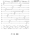
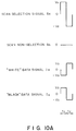
- Figure 4A shows a scanning selection signal S S , a scanning non-selection signal S N , a white data signal I W and a black data signal I B .
- Figure 4B shows a voltage waveform (I W - S S ) applied to a selected pixel (receiving a white data signal I W ) among the pixels (intersections between scanning electrodes and data electrodes) on a selected scanning electrode receiving a scanning selection signal S S , a voltage waveform (I B - S S ) applied to a non-selected pixel (receiving a black data signal I B ) on the same selected scanning electrode, and voltage waveforms applied to two types of pixels on non-selected scanning electrodes receiving a scanning non-selection signal S N .
- a non-selected pixel on a selected scanning electrode is supplied with a voltage -(V 1 +V 3 ) exceeding one threshold voltage of the ferroelectric liquid crystal to have the ferroelectric liquid crystal assume one orientation state providing a dark state, thus being written in "black".
- a selected pixel on the selected scanning electrode is supplied with a voltage (-V 1 +V 3 ) not exceeding the threshold voltages of the ferroelectric liquid crystal so that the orientation state of the ferroelectric liquid crystal is not changed.
- a phase t 2 the selected pixel on the selected scanning electrode is supplied with a voltage (V 2 + 3 ) exceeding the other threshold voltage of the ferroelectric liquid crystal to have the ferroelectric liquid crystal assume the other orientation state providing a bright state thus being written in "white". Further, in the phase t 2 , the non-selected pixel on the selected pixel is supplied with a voltage (V 2 -V 3 ) below the threshold voltages of the ferroelectric liquid crystal to retain the orientation state which is provided in the previous phase t 1 . On the other hand, in phases t 1 and t 2 , the pixels on non-selected scanning electrodes are supplied with voltages ⁇ V 3 below the threshold voltages of the ferroelectric liquid crystal.
- the pixels on the selected scanning electrode are written in "white” or “black” in a writing phase T 1 including the phases t 1 and t 2 , and the pixels retain their written states even when they subsequently receive a scanning non-selection signal.
- phase T 2 of this embodiment voltages having polarities opposite to those of the data signals in the writing phase T 1 are applied through the data electrodes.
- the pixels on the non-selected scanning electrodes are supplied with an AC voltage so that the threshold characteristic of the ferroelectric liquid crystal is improved.
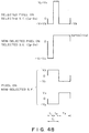
- Figure 4C is a time chart of a set of voltage waveforms providing a display state shown in Figure 5.
- a scanning selection signal is applied to the scanning electrodes with skipping of 5 lines apart in a field (one vertical scanning) and the scanning selection signal is applied to scanning electrodes which are not adjacent to each other in consecutive 6 fields.
- the scanning electrodes are selected 5 lines (electrodes) apart so that one frame scanning (one picture scanning) is effected in 6 fields of scanning (6 times of one vertical scanning).
- FIG 4D shows another embodiment using drive waveforms shown in Figure 4A.
- the scanning electrodes are selected two lines apart so that not-adjacent scanning electrodes are selected in consecutive three fields of scanning.
- Figures 6A and 6B show another driving embodiment used in the present invention.
- "black” is written in phase t 1 and "white” is written in phase t 2 .
- an auxiliary signal is applied through data electrodes so as to apply an AC voltage to the pixels at the time of non-selection similarly as in the previous embodiment.
- Such an auxiliary signal shows the effect as disclosed in U.S. Patent No. 4,655,561, etc.
- Figure 6C is a time chart showing application of scanning selection signals using driving waveforms shown in Figures 6A and 6B.
- the scanning selection signal is applied to the scanning electrodes with skipping of 7 lines apart and one frame scanning is completed in 8 fields of scanning. Also in this embodiment, the scanning selection signal is applied to not-adjacent scanning electrodes in consecutive 8 fields of scanning.
- a scanning selection signal may be applied to the scanning electrodes with skipping of 4 or more lines apart, preferably 5 - 20 lines apart.
- the peak values of the voltage signals V 1 , -V 2 and ⁇ V 3 may preferably be set to satisfy the relation of
- the pulse durations of these voltage signals may be set to 1 ⁇ sec - 1 msec, preferably 10 ⁇ sec - 100 ⁇ sec, and it is preferred to set a longer pulse duration at a lower temperature than at a higher temperature.
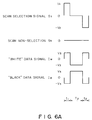
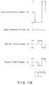
- Figures 7A and 7B show a set of driving waveforms in another embodiment. More specifically, Figure 7A shows a scanning selection signal S S , a scanning non-selection signal S N , a white data signal I W and a black data signal I B .
- Figure 4B shows a voltage waveform (I W - S S ) applied to a selected pixel (receiving a white data signal I W ) among the pixels (intersections between scanning electrodes and data electrodes) on a selected scanning electrode receiving a scanning selection signal S S , a voltage waveform (I B - S S ) applied to a non-selected signal (receiving a black data signal I B ) on the same selected scanning electrode, and voltage waveforms applied to two types of pixels on non-selected scanning electrodes receiving a scanning non-selection signal S N .
- the scanning electrodes prior to application of the above-mentioned scanning selection signal S S , are supplied with a clearing voltage signal V H which has a polarity opposite to that of the scanning selection signal S S (with respect to the voltage level of a non-selected scanning electrode) and has a voltage exceeding one threshold voltage of a ferroelectric liquid crystal, whereby the related pixels are oriented in advance to one orientation state of the ferroelectric liquid crystal to form a dark state, thus effecting a step of clearing into a "black” state.
- a selected pixel on a selected scanning electrode is supplied with a voltage -(V 1 + V 2 ) exceeding the other threshold voltage of the ferroelectric liquid crystal to result in a bright state based on the other orientation state of the ferroelectric liquid crystal, thus being written in "white".
- a non-selected pixel on the selected scanning electrode is supplied with a voltage (-V 1 + V 2 ) below the threshold voltages of the ferroelectric liquid crystal so that the orientation state of the ferroelectric liquid crystal is not changed thereby.
- the pixels on the non-selected scanning electrodes are supplied with voltages ⁇ V 2 which are below the threshold voltages of the ferroelectric liquid crystal in the phase t 1 .
- the pixels on the selected scanning electrode are written in either "white” or “black”, and the resultant states are retained even under subsequent application of scanning non-selection signals.
- phase t 2 of this embodiment voltages of polarities opposite to those of the data signals in phase t 1 are applied through the data electrodes.
- the pixels at the time of non-selection are supplied with an AC voltage so that the threshold characteristic of the ferroelectric liquid crystal can be improved.
- Figure 7C is a time for providing a display state shown in Figure 5 by using the driving waveforms shown in Figures 7A and 7B.
- a clearing voltage V H is applied to the scanning electrodes, and then the scanning selection signal is applied to the scanning electrodes (with skipping of) 5 lines apart so that the scanning selection is applied to scanning electrodes which are not adjacent to each other in consecutive 6 fields.
- the scanning electrodes are selected 5 lines apart so that one frame scanning (one picture scanning) is effected in 6 fields of scanning.
- FIG 7D shows another embodiment using the drive waveforms shown in Figures 7A and 7B.
- the scanning electrodes are selected two lines apart so that not-adjacent scanning electrodes are selected in consecutive three fields of scanning.
- Figure 7E shows another embodiment using the drive waveforms shown in Figures 7A and 7B, wherein only scanning signals are shown along with corresponding states of terminals Q 1 and Q 2 shown in Figure 8.
- one block is designated for 5 scanning electrodes each, and for each block, a clearing step is performed by application of a clearing voltage signal V H and then a scanning selection signal is sequentially applied to not-adjacent scanning electrodes.
- FIG 8 is a partial circuit diagram showing an output stage of a scanning electrode drive circuit for performing the drive of the above embodiment.
- the output stage includes terminals R 1 - R 5 , buffers 81 (B 1 - B 10 ...) connected to output lines S 1 - S 10 , and terminals Q 1 and Q 2 connected to the buffers 81 through selection lines 82.
- the output level of a buffer 81 is controlled by a selection line 82.
- buffers B 1 - B 5 are simultaneously turned on so as to transfer the levels of terminals R 1 - R 5 as they are to output lines S 1 - S 5 .
- the output lines S 1 - S 5 are all brought to a prescribed constant level so as to make the cells non-selective.
- a terminal Q 1 has the same function with respect to the buffers B 6 - B 10 .
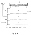
- FIG. 9 is a block diagram of a circuit for use in another embodiment of the present invention.
- data signals are supplied to a display panel 90 through a common data electrode drive circuit 91.
- a scanning electrode drive circuit 92 is divided into three sections #1, #2 and #3 so as to control display areas A, B and C, respectively, of the display panel 90.
- the scanning electrode drive circuits #1 - #3 are separately composed of their own logic circuits, and scanning electrodes for writing are first selected by input signals Q 1 - Q 3 and used to write in the areas A, B and C separately, so that writing of a large capacity and high density can be performed at a high speed.
- FIGS 10A and 10B show a set of driving waveforms used in another embodiment of the present invention. Similarly as in the previous embodiment, prior to application of a scanning selection signal, a clearing voltage V H is applied, so that the whole picture area or a block thereof is cleared into "black” (or "white”).
- Figure 10C is a time chart showing a time relation of applying scanning selection signals using the driving waveforms shown in Figures 10A and 10B, wherein only scanning selection signals are shown.
- a scanning selection signal is applied to the scanning electrodes with skipping of 6 lines apart so that one frame scanning is completed in 7 fields of scanning. Also in this embodiment, the scanning selection signal is applied to scanning electrodes which are not adjacent to each other in consecutive 7 fields of scanning.
- a scanning selection signal may be applied to 4 or more lines apart, preferably 5 - 20 lines apart.
- Figure 10D shows another embodiment using the driving waveforms shown in Figures 10A and 10B, wherein only scanning signals are shown.
- one block is designated for each 5 scanning electrodes, and for each block, a clearing step is performed by applying a clearing voltage signal V H , followed by sequential application of a scanning selection signal to scanning electrodes which are not adjacent to each other.
- one picture scanning is performed by sequentially effecting block scanning operations for blocks which are not adjacent to each other.
- the peak values of the voltage signals V H , V 1 and ⁇ V 2 in Figures 7A - 7E may preferably be set to satisfy the relations of:
- the peak values of the voltage signals V H , V 1 , -V 2 and ⁇ V 3 may preferably be set to satisfy the relations of:
- the pulse durations of these voltage signals in Figures 7 and 10 may be set to 1 ⁇ sec - 1 msec, preferably 10 ⁇ sec - 100 ⁇ sec and it is preferred to set a longer pulse duration at a lower temperature than at a high temperature.
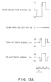
- Figure 11A shows a scanning selection signal S S , a scanning non-selection signal S N , a white data signal I W and a black data signal I B in another embodiment of the present invention.
- Figure 11B shows a voltage waveform (I W - S S ) applied to a selected pixel (receiving a white data signal I W ) among the pixels (intersections between scanning electrodes and data electrodes) on a selected scanning electrode receiving a scanning selection signal S S , a voltage waveform (I B - S S ) applied to a non-selected signal (receiving a black data signal I B ) on the same selected scanning electrode, and voltage waveforms applied to two types of pixels on non-selected scanning electrodes receiving a scanning non-selection signal S N .
- a phase T 1 is used for causing one orientation state of a ferroelectric liquid crystal regardless of the types of data pulses.
- cross nicol polarizers are set so as to provide a black display based on a dark state when the ferroelectric liquid crystal assumes one orientation state, but it is also possible to set the polarizers so as to provide a bright state corresponding to one orientation state.
- a former (sub-)phase t 1 in the phase T 1 is used as a phase for applying a part of a data signal applied in association with a previous scanning selection signal.
- phase t 3 a selected pixel on a selected scanning electrode receiving a scanning selection signal S S is supplied with a voltage -(V 1 +V 3 ) to result in the other orientation state of the ferroelectric liquid crystal, whereby a white display based on a bright state is given after clearing into a "black" display in the phase T 1 .
- another pixel (non-selected pixel) on the selected scanning electrode is supplied with a voltage -(V 1 -V 3 ) which however is set to a voltage not changing the orientation state of the ferroelectric liquid crystal, so that the black display state resultant in the phase T 1 is retained in the phase t 3 .
- the pixels on the non-selected scanning electrodes receiving a scanning non-selection signal are supplied with voltages ⁇ V 3 not changing the orientation states of the ferroelectric liquid crystal.
- the written states are retained as they are during one field or frame scanning period.
- phase t 2 of this embodiment voltages having polarities opposite to those of the data pulses in the writing phase t 3 are applied through the data electrodes.
- the pixels on the non-selected scanning electrodes are supplied with an AC voltage, so that the threshold characteristic of the ferroelectric liquid crystal is improved.
- Figure 11C is a time chart of a set of voltage waveforms providing a display state as shown in Figure 5 with respect to scanning electrodes S 1 - S 8 .
- a scanning selection signal is applied to the scanning electrodes with skipping of 3 lines apart in a field and the scanning selection signal is applied to scanning electrodes which are not adjacent to each other in consecutive 4 fields.
- the scanning electrodes are selected 3 lines apart, so that one frame scanning (one picture scanning) is performed in 4 fields of scanning.
- FIG 11D shows another embodiment using drive waveforms shown in Figure 11A.
- the scanning electrodes are selected 5 lines apart so that not-adjacent scanning electrodes are selected in consecutive 6 fields of scanning.
- the scanning pulses and data pulses are set to satisfy the relationships of
- 3
- These relationships are not necessarily essential, but for example, a relationship of
- a
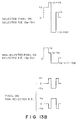
- Figures 12A and 12B show a set of driving waveforms used in another driving embodiment.
- all or a prescribed number of the pixels on a selected scanning electrode are cleared into "black" in phase T 1 regardless of the types of data signals concerned, and in writing phase t 3 , a selected pixel among the pixels is supplied with a voltage providing a white display and the other pixels among the pixels are supplied with a voltage maintaining the black display.
- Phase t 4 is a phase for applying auxiliary signals through the data electrodes so as to always apply an AC voltage to the pixels at the time of non-selection, and these auxiliary signals correspond to a part of data signals for previous data entry applied in phase t 1 .
- the effect of application of such an auxiliary signal has been classified, e.g., in U.S. Patent No. 4,655,561.
- Figure 12C is a time chart of a set of voltage waveforms using those shown in Figures 12A and 12B for providing a display state as shown in Figure 5, with respect to scanning electrodes S 1 - S 8 .
- a scanning selection signal is applied to the scanning electrodes with skipping of 3 lines apart and one frame scanning is completed by 4 fields of scanning.
- the scanning selection signal is applied to scanning electrodes which are not adjacent to each other in four scanning fields.
- a former pulse (voltage: -V 2 ) of a subsequent scanning selection signal is applied immediately after application of a latter pulse (voltage: V 1 ) of a preceding scanning selection signal.
- Phase T 1 is a clearing phase similar to the one in the previous embodiment and phase t 3 is a writing phase similar to the one in the previous embodiment.
- Phases t 2 and t 4 correspond to phases for applying auxiliary signals used in the previous embodiment so as to always apply AC voltages to pixels at the time of non-selection, whereby the threshold characteristic of the ferroelectric liquid crystal is improved.
- phase t 1 is also used for applying a part of a data signal associated with a previous scanning selection signal.
- Figure 13C is a time chart of a set of voltage waveforms using those shown in Figures 13A and 13B for providing a display state as shown in Figure 5, with respect to scanning electrodes S 1 - S 12 .
- a scanning selection signal is applied to the scanning electrodes with skipping of 5 lines apart and one frame scanning is completed by 6 fields of scanning.
- the scanning selection signal is applied to scanning electrodes which are not adjacent to each other in 6 scanning fields.
- a former pulse (voltage: -V 2 ) of a subsequent scanning selection signal is applied immediately after application of a latter pulse (voltage: V 1 ) of a preceding scanning selection signal.
- a former pulse of a subsequent scanning selection signal is applied simultaneously with or immediately after the application of a latter pulse of a previous scanning selection signal, and also the subsequent scanning selection signal is applied before the completion of a data signal applied for data entry associated with the previous scanning selection signal.
- a scanning selection signal may be applied to the scanning electrodes with skipping of 4 or more lines apart, preferably 5 - 20 lines apart.
- the peak values of the voltage signals V 1 , -V 2 and ⁇ V 3 may preferably be set to satisfy the relation of
- the pulse durations of these voltage signals may be set to 1 ⁇ sec - 1 msec, preferably 10 ⁇ sec - 100 ⁇ sec, and it is preferred to set a longer pulse duration at a lower temperature than at a higher temperature.
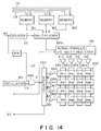
- Figure 14 is a circuit diagram showing a liquid crystal display drive control system used in the present invention.
- the memories M 1 , M 2 and M 3 are supplied with data through a data bus DB and are controlled through a control bus CB with respect to writing/readout and addressing.
- the system further includes a decoder DC to which a field switching signal FC is supplied, a multiplier MPX for selecting one of the outputs from the memories M1, M2 and M3, a monostable multi-vibrator MM supplying a gate signal GT to an AND gate to which clock signals CK are also supplied from a clock pulse oscillator FG, a counter CNT to which now-scanning clock signals F are supplied from the AND gate, a serial input/parallel output shift register SR, a column drive circuits DR 1 - DR 4 and row drive circuits DR 5 - DR 8 .
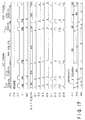
- Figure 15 shows gradation data for respective pixels for one gradational picture scanning (referred to as "one frame").
- the highest level bit HSB, the medium level but MSB and the lowest level bit LSB of each gradation data are inputted to the memories M3, M2 and M1, respectively, through the data but DB.
- one picture scanning (referred to as "one sub-frame") switching signal FC is generated at time t 1
- the decoder DC sets the multiplexer MPX to receive data from the memory M1.
- the signal FC is inputted to the monostable multi-vibrator MM to generate a gate signal GT and open the AND gate, thereby to supply four clock signals CK as a row scanning signal F to the counter CNT.
- the counter CNT turns the driver DR5 on receiving the first clock signal.
- the shift register SR is loaded with the first row data of the memory M1, and only the driver DR3 is made on.
- a liquid crystal pixel A 13 alone is set to a dark level and the other liquid crystal pixels A 11 , A 12 and A 14 are set to a bright level.
- the row scanning signal F is inputted to a controller (not shown) as a memory row scanning signal
- the memory M1 supplies subsequent second row data to the shift register
- the driver DR6 is turned on receiving a subsequent row scanning signal F
- the second row data of the memory M1 are respectively supplied to the drivers DR1 - DR4 from the shift register SR.
- the drivers DR2, DR3 and DR4 are turned on to set the pixels A 22 , A 23 and A 24 to the dark level and the pixel A 21 to the bright level.
- the above operations are repeated for the third and fourth rows.
- the counter CNT supplies a memory switching demand signal MC to a controller (not shown) to select the memory M2 to start a second sub-frame.
- the respective liquid crystal pixels set to bright or dark states retain their states because the ferroelectric liquid crystal has a memory function.
- the multiplexer MPX selects data from the memory M2 based on a sub-frame switching signal FC, and a row scanning signal F is supplied to the counter CNT and the shift register SR based on a gate signal GT. Then, row scanning is performed in a similar cycle as in the first sub-frame to set the respective liquid crystal pixels to dark or bright states.
- a third frame is performed in a similar manner.
- the periods of the first, second and third sub-frames are set to ratios of 1:2:4 in the same values as the weights of the respective bits.
- the gradation data for, e.g., the pixel A 12 is 2 as shown in Figure 16D, so that the pixel A 12 is set to the dark level only in the second sub-frame period and assumers the dark state for 2/7 of one frame period.
- the gradation data for the pixel A 24 is 5, so that the pixel A 24 is set to the dark level for the first and third sub-frame periods and assumes the dark state for 5/7 of one frame period.
- the gradation data for the pixel A 42 is 7, so that the pixel A 42 is caused to assume the dark state for all the sub-frame periods.
- gradational display at 8 levels can be performed in this embodiment.
- an apparent intermediate toner or gray scale can be displayed by controlling the proportion of a display time in one frame period, i.e., a display duty.
- an intermediate gradational display can be generally performed if one frame is divided into a plurality, i.e., two or more, of sub-frames.
- the sub-frame periods are set to have different durations corresponding to the weights of data bits in the above embodiments, but the sub-frames can also be provided with equal durations by equal division. In this case, however, it is necessary to decode gradation data.
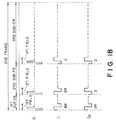
- Figure 18 shows examples of drive waveforms applied to a scanning electrode S 1 and data electrodes I 1 and I 2 in one frame and first to third sub-frames contained therein.
- the first, second and third sub-frames are set to have duration ratios of 1:2:4, respectively.
- the intersection of the scanning electrode S 1 and data electrode I 1 is provided with a gradational display corresponding to a weighted total of BR (bright) in the first sub-frame, BR in the second sub-frame and D (dark) in the third sub-frame.
- intersection of the scanning electrode S 1 and data electrode I 2 is provided with a gradational display corresponding to a weighted total of BR in the first sub-frame, D in the second sub-frame and D in the third sub-frame. Further, in this embodiment, the intersection of the scanning electrode S 1 and data electrode I 2 is set to have an area which is two times that of the intersection of the scanning electrode S 1 and data electrode I 1 , and an increased variety of gradational display is performed based on such intersectional area ratios.
- various ferroelectric liquid crystal devices can be used, including an SSFLC device as disclosed by Clark et al in U.S. Patent No. 4,367,924, a ferroelectric liquid crystal device in an alignment state retaining a helical residue as disclosed by Isogai et al in U.S. Patent No. 4,586,791 and a ferroelectric liquid crystal device in an alignment state as disclosed in U.K. Patent GB-A 2159635.
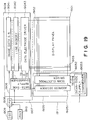
- FIG. 19 is a block diagram illustrating a structural arrangement of an embodiment of the display apparatus according to the present invention.
- a display panel 1901 is composed of scanning electrodes 1902, data electrodes 1903 and a ferroelectric liquid crystal disposed therebetween. The orientation of the ferroelectric liquid crystal is controlled by an electric field at each intersection of the scanning electrodes 1902 and data electrodes 1903 formed due to voltages applied across the electrodes.
- the display apparatus includes a data electrode driver circuit 1904, which in turn comprises an image data shift register 19041 for storing image data serially supplied from a data signal line 1906, a line memory 19042 for storing image data supplied in parallel from the image data shift register 19041, a data electrode driver 19043 for supplying voltages to data electrodes 1903 according to the image data stored in the line memory 19042, and a data side power supply changeover unit 19044 for changing over among voltages V D , 0 and -V D supplied to the data electrodes 1903 based on a signal from a changeover control line 1911.
- a data electrode driver circuit 1904 which in turn comprises an image data shift register 19041 for storing image data serially supplied from a data signal line 1906, a line memory 19042 for storing image data supplied in parallel from the image data shift register 19041, a data electrode driver 19043 for supplying voltages to data electrodes 1903 according to the image data stored in the line memory 19042, and a data side power
- the display apparatus further includes a scanning electrode driver circuit 1905, which in turn comprises a decoder 19051 for designating a scanning electrode among all the scanning electrodes based on a signal received from a scanning address data line 1907, a scanning electrode driver 19052 for applying voltages to the scanning electrodes 1902 based on a signal from the decoder 19051, and a scanning side power supply changeover unit 19053 for changing over among voltages V S , 0 and -V S supplied to the scanning electrodes 1902 based on a signal from a changeover control line 1911.
- a scanning electrode driver circuit 1905 which in turn comprises a decoder 19051 for designating a scanning electrode among all the scanning electrodes based on a signal received from a scanning address data line 1907, a scanning electrode driver 19052 for applying voltages to the scanning electrodes 1902 based on a signal from the decoder 19051, and a scanning side power supply changeover unit 19053 for changing over among voltages V S , 0
- the display apparatus further includes a CPU 19019, which receives clock pulses from an oscillator 1909, controls the image memory 1910, and controls the signal transfer over the data signal line 1906, scanning address data line 1907 and changeover control line 1911.
- a CPU 19019 which receives clock pulses from an oscillator 1909, controls the image memory 1910, and controls the signal transfer over the data signal line 1906, scanning address data line 1907 and changeover control line 1911.
- the present invention it is possible to effectively suppress the occurrence of flicker caused by scanning drive at a low frame frequency as low as 2 - 15 Hz. Particularly, the occurrence of flicker is prevented for a long scanning selection period set at a low temperature, whereby it is possible to provide a high-quality display picture over a substantially wide temperature range. According to the present invention, it is further possible to effectively prevent a phenomenon of image flow, whereby a high-quality display picture, particularly gradational display picture, can be formed also in this respect.
- a liquid crystal apparatus includes: a) a liquid crystal device comprising an electrode matrix composed of scanning electrodes and data electrodes, and a ferroelectric liquid crystal showing a first and a second orientation state; and b) a driving means including: a first drive means for applying a scanning selection signal to the scanning electrodes two or more scanning electrodes apart in one vertical scanning so as to effect one picture scanning in plural times of vertical scanning, said scanning selection signal having a voltage of one polarity and a voltage of the other polarity with respect to the voltage level of a nonselected scanning electrode, and a second drive means for applying to a selected data electrode a voltage signal which provides a voltage causing the first orientation state of the ferroelectric liquid crystal in combination with the voltage of one polarity of the scanning selection signal, and applying to another data electrode a voltage signal which provides a voltage causing the second orientation state of the ferroelectric liquid crystal in combination with the voltage of the other polarity of the scanning selection signal.
Landscapes
- Engineering & Computer Science (AREA)
- Chemical & Material Sciences (AREA)
- Crystallography & Structural Chemistry (AREA)
- Physics & Mathematics (AREA)
- Computer Hardware Design (AREA)
- General Physics & Mathematics (AREA)
- Theoretical Computer Science (AREA)
- Liquid Crystal Display Device Control (AREA)
- Liquid Crystal (AREA)
Applications Claiming Priority (13)
| Application Number | Priority Date | Filing Date | Title |
|---|---|---|---|
| JP27181288 | 1988-10-26 | ||
| JP271813/88 | 1988-10-26 | ||
| JP271812/88 | 1988-10-26 | ||
| JP27181388A JP2578490B2 (ja) | 1988-10-26 | 1988-10-26 | 表示装置の駆動法 |
| JP27181288A JP2575198B2 (ja) | 1988-10-26 | 1988-10-26 | 表示装置の駆動法 |
| JP27181388 | 1988-10-26 | ||
| JP28012388 | 1988-11-05 | ||
| JP280122/88 | 1988-11-05 | ||
| JP63280122A JP2637515B2 (ja) | 1988-11-05 | 1988-11-05 | 液晶装置及び液晶素子の駆動法 |
| JP28012388A JP2608318B2 (ja) | 1988-11-05 | 1988-11-05 | 液晶装置 |
| JP28012288 | 1988-11-05 | ||
| JP280123/88 | 1988-11-05 | ||
| EP89119844A EP0366117B1 (de) | 1988-10-26 | 1989-10-25 | Flüssigkristall-Vorrichtung |
Related Parent Applications (2)
| Application Number | Title | Priority Date | Filing Date |
|---|---|---|---|
| EP89119844A Division EP0366117B1 (de) | 1988-10-26 | 1989-10-25 | Flüssigkristall-Vorrichtung |
| EP89119844.2 Division | 1989-10-25 |
Publications (3)
| Publication Number | Publication Date |
|---|---|
| EP0726556A2 true EP0726556A2 (de) | 1996-08-14 |
| EP0726556A3 EP0726556A3 (de) | 1998-08-26 |
| EP0726556B1 EP0726556B1 (de) | 2000-06-07 |
Family
ID=27478936
Family Applications (2)
| Application Number | Title | Priority Date | Filing Date |
|---|---|---|---|
| EP95120037A Expired - Lifetime EP0726556B1 (de) | 1988-10-26 | 1989-10-25 | Flüssigkristallanzeigevorrichtung |
| EP89119844A Expired - Lifetime EP0366117B1 (de) | 1988-10-26 | 1989-10-25 | Flüssigkristall-Vorrichtung |
Family Applications After (1)
| Application Number | Title | Priority Date | Filing Date |
|---|---|---|---|
| EP89119844A Expired - Lifetime EP0366117B1 (de) | 1988-10-26 | 1989-10-25 | Flüssigkristall-Vorrichtung |
Country Status (4)
| Country | Link |
|---|---|
| US (2) | US5233447A (de) |
| EP (2) | EP0726556B1 (de) |
| AT (2) | ATE193780T1 (de) |
| DE (2) | DE68926771T2 (de) |
Cited By (1)
| Publication number | Priority date | Publication date | Assignee | Title |
|---|---|---|---|---|
| WO2019019312A1 (zh) * | 2017-07-24 | 2019-01-31 | 惠科股份有限公司 | 显示面板的驱动方法、驱动装置及显示装置 |
Families Citing this family (63)
| Publication number | Priority date | Publication date | Assignee | Title |
|---|---|---|---|---|
| US5233447A (en) * | 1988-10-26 | 1993-08-03 | Canon Kabushiki Kaisha | Liquid crystal apparatus and display system |
| US5815130A (en) * | 1989-04-24 | 1998-09-29 | Canon Kabushiki Kaisha | Chiral smectic liquid crystal display and method of selectively driving the scanning and data electrodes |
| DE4017893A1 (de) * | 1990-06-02 | 1991-12-05 | Hoechst Ag | Verfahren zur ansteuerung eines ferroelektrischen fluessigkristalldisplays |
| DE69113150T2 (de) * | 1990-06-29 | 1996-04-04 | Texas Instruments Inc | Deformierbare Spiegelvorrichtung mit aktualisiertem Raster. |
| US6097357A (en) * | 1990-11-28 | 2000-08-01 | Fujitsu Limited | Full color surface discharge type plasma display device |
| JP3259253B2 (ja) * | 1990-11-28 | 2002-02-25 | 富士通株式会社 | フラット型表示装置の階調駆動方法及び階調駆動装置 |
| US6787995B1 (en) | 1992-01-28 | 2004-09-07 | Fujitsu Limited | Full color surface discharge type plasma display device |
| JP2942092B2 (ja) * | 1993-04-20 | 1999-08-30 | キヤノン株式会社 | 液晶素子の制御方法 |
| EP0632425A1 (de) * | 1993-06-29 | 1995-01-04 | Central Research Laboratories Limited | Adressierung einer Matrix von bistabiler Pixeln |
| JP3307486B2 (ja) * | 1993-11-19 | 2002-07-24 | 富士通株式会社 | 平面表示装置及びその制御方法 |
| JP3059048B2 (ja) * | 1994-05-19 | 2000-07-04 | シャープ株式会社 | 液晶表示装置及びその駆動方法 |
| JP3653732B2 (ja) * | 1994-06-03 | 2005-06-02 | セイコーエプソン株式会社 | 液晶表示装置の駆動方法,液晶表示装置,電子機器及び駆動回路 |
| JP3897826B2 (ja) * | 1994-08-19 | 2007-03-28 | 株式会社半導体エネルギー研究所 | アクティブマトリクス型の表示装置 |
| JP3184069B2 (ja) * | 1994-09-02 | 2001-07-09 | シャープ株式会社 | 画像表示装置 |
| EP0703561A3 (de) * | 1994-09-26 | 1996-12-18 | Canon Kk | Verfahren und Einrichtung zum Steuern eines Anzeigegeräts |
| JP3058804B2 (ja) | 1994-11-16 | 2000-07-04 | キヤノン株式会社 | 液晶装置 |
| US5748164A (en) | 1994-12-22 | 1998-05-05 | Displaytech, Inc. | Active matrix liquid crystal image generator |
| US5757348A (en) * | 1994-12-22 | 1998-05-26 | Displaytech, Inc. | Active matrix liquid crystal image generator with hybrid writing scheme |
| US5808800A (en) | 1994-12-22 | 1998-09-15 | Displaytech, Inc. | Optics arrangements including light source arrangements for an active matrix liquid crystal image generator |
| US6229515B1 (en) * | 1995-06-15 | 2001-05-08 | Kabushiki Kaisha Toshiba | Liquid crystal display device and driving method therefor |
| FR2745411B1 (fr) * | 1996-02-27 | 1998-04-03 | Thomson Csf | Procede de commande d'un ecran de visualisation d'image utilisant le principe de la modulation de duree d'emission de lumiere, et dispositif de visualisation mettant en oeuvre le procede |
| JP3560756B2 (ja) * | 1997-02-13 | 2004-09-02 | アルプス電気株式会社 | 表示装置の駆動方法 |
| JP3559719B2 (ja) | 1998-01-13 | 2004-09-02 | キヤノン株式会社 | プラズマアドレス型の液晶表示装置 |
| JP3347678B2 (ja) | 1998-06-18 | 2002-11-20 | キヤノン株式会社 | 液晶素子とその駆動方法 |
| US6670937B1 (en) | 1999-03-01 | 2003-12-30 | Canon Kabushiki Kaisha | Liquid crystal display apparatus |
| US6545656B1 (en) * | 1999-05-14 | 2003-04-08 | Semiconductor Energy Laboratory Co., Ltd. | Liquid crystal display device in which a black display is performed by a reset signal during one sub-frame |
| US7348953B1 (en) | 1999-11-22 | 2008-03-25 | Semiconductor Energy Laboratory Co., Ltd. | Method of driving liquid crystal display device |
| US7129918B2 (en) * | 2000-03-10 | 2006-10-31 | Semiconductor Energy Laboratory Co., Ltd. | Electronic device and method of driving electronic device |
| US7385579B2 (en) * | 2000-09-29 | 2008-06-10 | Semiconductor Energy Laboratory Co., Ltd. | Liquid crystal display device and method of driving the same |
| JP2002201473A (ja) | 2000-10-25 | 2002-07-19 | Canon Inc | スメクチック高分子液晶及びその製造方法、これを用いた液晶素子 |
| JP2002236472A (ja) * | 2001-02-08 | 2002-08-23 | Semiconductor Energy Lab Co Ltd | 液晶表示装置およびその駆動方法 |
| JP4831892B2 (ja) * | 2001-07-30 | 2011-12-07 | 株式会社半導体エネルギー研究所 | 半導体装置 |
| US7554535B2 (en) * | 2001-10-05 | 2009-06-30 | Nec Corporation | Display apparatus, image display system, and terminal using the same |
| US20030117382A1 (en) * | 2001-12-07 | 2003-06-26 | Pawlowski Stephen S. | Configurable panel controller and flexible display interface |
| JP2005529366A (ja) * | 2002-06-11 | 2005-09-29 | コーニンクレッカ フィリップス エレクトロニクス エヌ ヴィ | ディスプレイにおけるライン走査 |
| WO2004086343A1 (ja) | 2003-03-26 | 2004-10-07 | Semiconductor Energy Laboratory Co., Ltd. | 素子基板及び発光装置 |
| US7019884B2 (en) * | 2003-03-31 | 2006-03-28 | Intel Corporation | Light modulator with bi-directional drive |
| WO2004109643A1 (en) * | 2003-06-05 | 2004-12-16 | Koninklijke Philips Electronics N.V. | Display device addressing method |
| US7683860B2 (en) * | 2003-12-02 | 2010-03-23 | Semiconductor Energy Laboratory Co., Ltd. | Display device, driving method thereof, and element substrate |
| US7706050B2 (en) | 2004-03-05 | 2010-04-27 | Qualcomm Mems Technologies, Inc. | Integrated modulator illumination |
| US20050205880A1 (en) * | 2004-03-19 | 2005-09-22 | Aya Anzai | Display device and electronic appliance |
| WO2005114630A1 (en) * | 2004-05-21 | 2005-12-01 | Semiconductor Energy Laboratory Co., Ltd. | Display device and electronic device |
| US7332742B2 (en) * | 2004-06-29 | 2008-02-19 | Semiconductor Energy Laboratory Co., Ltd. | Display device and electronic apparatus |
| US7355780B2 (en) | 2004-09-27 | 2008-04-08 | Idc, Llc | System and method of illuminating interferometric modulators using backlighting |
| US8102407B2 (en) | 2004-09-27 | 2012-01-24 | Qualcomm Mems Technologies, Inc. | Method and device for manipulating color in a display |
| US7813026B2 (en) | 2004-09-27 | 2010-10-12 | Qualcomm Mems Technologies, Inc. | System and method of reducing color shift in a display |
| US7911428B2 (en) | 2004-09-27 | 2011-03-22 | Qualcomm Mems Technologies, Inc. | Method and device for manipulating color in a display |
| US8362987B2 (en) | 2004-09-27 | 2013-01-29 | Qualcomm Mems Technologies, Inc. | Method and device for manipulating color in a display |
| US8031133B2 (en) | 2004-09-27 | 2011-10-04 | Qualcomm Mems Technologies, Inc. | Method and device for manipulating color in a display |
| US7525730B2 (en) | 2004-09-27 | 2009-04-28 | Idc, Llc | Method and device for generating white in an interferometric modulator display |
| US7710632B2 (en) | 2004-09-27 | 2010-05-04 | Qualcomm Mems Technologies, Inc. | Display device having an array of spatial light modulators with integrated color filters |
| US7932877B2 (en) | 2004-11-24 | 2011-04-26 | Semiconductor Energy Laboratory Co., Ltd. | Display device and electronic apparatus |
| JP4182100B2 (ja) * | 2004-12-15 | 2008-11-19 | キヤノン株式会社 | アクティブマトリクス液晶表示装置 |
| US7616179B2 (en) * | 2006-03-31 | 2009-11-10 | Canon Kabushiki Kaisha | Organic EL display apparatus and driving method therefor |
| US8004743B2 (en) | 2006-04-21 | 2011-08-23 | Qualcomm Mems Technologies, Inc. | Method and apparatus for providing brightness control in an interferometric modulator (IMOD) display |
| KR101315380B1 (ko) * | 2006-10-16 | 2013-10-07 | 삼성디스플레이 주식회사 | 디스플레이장치 및 그 제어방법 |
| WO2009098705A1 (en) * | 2008-02-07 | 2009-08-13 | Raman Research Institute | A method to display gray shades in rms responding matrix display |
| WO2010050511A1 (ja) * | 2008-10-30 | 2010-05-06 | シャープ株式会社 | 液晶表示駆動回路および液晶表示装置 |
| US8848294B2 (en) | 2010-05-20 | 2014-09-30 | Qualcomm Mems Technologies, Inc. | Method and structure capable of changing color saturation |
| JP5724243B2 (ja) | 2010-08-19 | 2015-05-27 | セイコーエプソン株式会社 | 液晶駆動装置、液晶表示装置、電子機器及び液晶駆動方法 |
| KR20150070683A (ko) * | 2013-12-17 | 2015-06-25 | 삼성디스플레이 주식회사 | 액정 표시 장치 및 이의 구동 방법 |
| US10916218B2 (en) * | 2016-06-30 | 2021-02-09 | Lg Display Co., Ltd. | Organic light emitting diode display |
| JP2022154077A (ja) * | 2021-03-30 | 2022-10-13 | 凸版印刷株式会社 | 表示装置 |
Citations (6)
| Publication number | Priority date | Publication date | Assignee | Title |
|---|---|---|---|---|
| JPS56107216A (en) | 1980-01-08 | 1981-08-26 | Clark Noel A | Liquid crystal electrooptical device and production thereof |
| EP0149899A2 (de) | 1983-12-09 | 1985-07-31 | Seiko Instruments Inc. | Flüssigkristallanzeigeeinrichtung |
| US4548476A (en) | 1983-01-14 | 1985-10-22 | Canon Kabushiki Kaisha | Time-sharing driving method for ferroelectric liquid crystal display |
| GB2159635A (en) | 1984-04-16 | 1985-12-04 | Canon Kk | Liquid crystal device |
| US4586791A (en) | 1982-04-07 | 1986-05-06 | Hitachi, Ltd. | Optical modulation element with surface parallel and unidirectional alignment of LC |
| US4655561A (en) | 1983-04-19 | 1987-04-07 | Canon Kabushiki Kaisha | Method of driving optical modulation device using ferroelectric liquid crystal |
Family Cites Families (13)
| Publication number | Priority date | Publication date | Assignee | Title |
|---|---|---|---|---|
| US4763995A (en) * | 1983-04-28 | 1988-08-16 | Canon Kabushiki Kaisha | Spacers with alignment effect and substrates having a weak alignment effect |
| JPS61204681A (ja) * | 1985-03-07 | 1986-09-10 | キヤノン株式会社 | 液晶パネル |
| US4778260A (en) * | 1985-04-22 | 1988-10-18 | Canon Kabushiki Kaisha | Method and apparatus for driving optical modulation device |
| US4836656A (en) * | 1985-12-25 | 1989-06-06 | Canon Kabushiki Kaisha | Driving method for optical modulation device |
| US4770502A (en) * | 1986-01-10 | 1988-09-13 | Hitachi, Ltd. | Ferroelectric liquid crystal matrix driving apparatus and method |
| GB8622717D0 (en) * | 1986-09-20 | 1986-10-29 | Emi Plc Thorn | Display device |
| JPS63225295A (ja) * | 1987-03-14 | 1988-09-20 | シャープ株式会社 | 液晶表示装置 |
| JP2670044B2 (ja) * | 1987-03-31 | 1997-10-29 | キヤノン株式会社 | 表示制御装置 |
| US5041821A (en) * | 1987-04-03 | 1991-08-20 | Canon Kabushiki Kaisha | Ferroelectric liquid crystal apparatus with temperature dependent DC offset voltage |
| JPS6442633A (en) * | 1987-08-10 | 1989-02-14 | Koito Mfg Co Ltd | Liquid crystal display device for color display |
| JP2612863B2 (ja) * | 1987-08-31 | 1997-05-21 | シャープ株式会社 | 表示装置の駆動方法 |
| JP2651204B2 (ja) * | 1988-07-14 | 1997-09-10 | キヤノン株式会社 | 液晶装置の駆動法 |
| US5233447A (en) * | 1988-10-26 | 1993-08-03 | Canon Kabushiki Kaisha | Liquid crystal apparatus and display system |
-
1989
- 1989-10-24 US US07/426,083 patent/US5233447A/en not_active Expired - Fee Related
- 1989-10-25 EP EP95120037A patent/EP0726556B1/de not_active Expired - Lifetime
- 1989-10-25 AT AT95120037T patent/ATE193780T1/de not_active IP Right Cessation
- 1989-10-25 EP EP89119844A patent/EP0366117B1/de not_active Expired - Lifetime
- 1989-10-25 DE DE68926771T patent/DE68926771T2/de not_active Expired - Fee Related
- 1989-10-25 DE DE68929223T patent/DE68929223T2/de not_active Expired - Fee Related
- 1989-10-25 AT AT89119844T patent/ATE140096T1/de not_active IP Right Cessation
-
1995
- 1995-01-18 US US08/375,181 patent/US5615027A/en not_active Expired - Fee Related
Patent Citations (7)
| Publication number | Priority date | Publication date | Assignee | Title |
|---|---|---|---|---|
| JPS56107216A (en) | 1980-01-08 | 1981-08-26 | Clark Noel A | Liquid crystal electrooptical device and production thereof |
| US4367924A (en) | 1980-01-08 | 1983-01-11 | Clark Noel A | Chiral smectic C or H liquid crystal electro-optical device |
| US4586791A (en) | 1982-04-07 | 1986-05-06 | Hitachi, Ltd. | Optical modulation element with surface parallel and unidirectional alignment of LC |
| US4548476A (en) | 1983-01-14 | 1985-10-22 | Canon Kabushiki Kaisha | Time-sharing driving method for ferroelectric liquid crystal display |
| US4655561A (en) | 1983-04-19 | 1987-04-07 | Canon Kabushiki Kaisha | Method of driving optical modulation device using ferroelectric liquid crystal |
| EP0149899A2 (de) | 1983-12-09 | 1985-07-31 | Seiko Instruments Inc. | Flüssigkristallanzeigeeinrichtung |
| GB2159635A (en) | 1984-04-16 | 1985-12-04 | Canon Kk | Liquid crystal device |
Cited By (1)
| Publication number | Priority date | Publication date | Assignee | Title |
|---|---|---|---|---|
| WO2019019312A1 (zh) * | 2017-07-24 | 2019-01-31 | 惠科股份有限公司 | 显示面板的驱动方法、驱动装置及显示装置 |
Also Published As
| Publication number | Publication date |
|---|---|
| DE68929223D1 (de) | 2000-07-13 |
| EP0726556B1 (de) | 2000-06-07 |
| EP0366117A3 (de) | 1991-05-08 |
| EP0366117A2 (de) | 1990-05-02 |
| DE68926771D1 (de) | 1996-08-08 |
| EP0366117B1 (de) | 1996-07-03 |
| EP0726556A3 (de) | 1998-08-26 |
| US5615027A (en) | 1997-03-25 |
| DE68926771T2 (de) | 1997-01-09 |
| ATE140096T1 (de) | 1996-07-15 |
| DE68929223T2 (de) | 2001-02-15 |
| US5233447A (en) | 1993-08-03 |
| ATE193780T1 (de) | 2000-06-15 |
Similar Documents
| Publication | Publication Date | Title |
|---|---|---|
| EP0726556B1 (de) | Flüssigkristallanzeigevorrichtung | |
| EP0606929B1 (de) | Flüssigkristallgerät | |
| US5929832A (en) | Memory interface circuit and access method | |
| US5136282A (en) | Ferroelectric liquid crystal apparatus having separate display areas and driving method therefor | |
| US4709995A (en) | Ferroelectric display panel and driving method therefor to achieve gray scale | |
| US6229583B1 (en) | Liquid crystal display device and method for driving the same | |
| US6252573B1 (en) | Drive method, a drive circuit and a display device for liquid crystal cells | |
| US6046717A (en) | Liquid crystal apparatus | |
| US5267065A (en) | Liquid crystal apparatus | |
| EP0581255B1 (de) | Verfahren und Einrichtung zum Steuern eines Flüssigkristallanzeigeelements | |
| US5408246A (en) | Electro-optical modulating apparatus and driving method thereof | |
| EP1410374B1 (de) | Anzeigetreibereinrichtungen und ansteuerverfahren | |
| US6597335B2 (en) | Liquid crystal display device and method for driving the same | |
| EP0607598B1 (de) | Verfahren und Einrichtung für eine Flüssigkristallanzeige | |
| US5815130A (en) | Chiral smectic liquid crystal display and method of selectively driving the scanning and data electrodes | |
| JPH10325946A (ja) | 光変調装置 | |
| US6028579A (en) | Driving method for liquid crystal devices | |
| JP2578490B2 (ja) | 表示装置の駆動法 | |
| JP2637515B2 (ja) | 液晶装置及び液晶素子の駆動法 | |
| JP2637517B2 (ja) | 液晶装置 | |
| JP2608318B2 (ja) | 液晶装置 | |
| US6118424A (en) | Method of driving antiferroelectric liquid crystal display | |
| EP0614563B1 (de) | Flüssigkristallanseigevorrichtung | |
| JP2575198B2 (ja) | 表示装置の駆動法 | |
| AU621252B2 (en) | Liquid crystal apparatus |
Legal Events
| Date | Code | Title | Description |
|---|---|---|---|
| PUAI | Public reference made under article 153(3) epc to a published international application that has entered the european phase |
Free format text: ORIGINAL CODE: 0009012 |
|
| AC | Divisional application: reference to earlier application |
Ref document number: 366117 Country of ref document: EP |
|
| AK | Designated contracting states |
Kind code of ref document: A2 Designated state(s): AT BE CH DE ES FR GB GR IT LI LU NL SE |
|
| PUAL | Search report despatched |
Free format text: ORIGINAL CODE: 0009013 |
|
| AK | Designated contracting states |
Kind code of ref document: A3 Designated state(s): AT BE CH DE ES FR GB GR IT LI LU NL SE |
|
| 17P | Request for examination filed |
Effective date: 19990108 |
|
| GRAG | Despatch of communication of intention to grant |
Free format text: ORIGINAL CODE: EPIDOS AGRA |
|
| RTI1 | Title (correction) |
Free format text: LIQUID CRYSTAL DISPLAY APPARATUS |
|
| RTI1 | Title (correction) |
Free format text: LIQUID CRYSTAL DISPLAY APPARATUS |
|
| RTI1 | Title (correction) |
Free format text: LIQUID CRYSTAL DISPLAY APPARATUS |
|
| 17Q | First examination report despatched |
Effective date: 19990805 |
|
| GRAG | Despatch of communication of intention to grant |
Free format text: ORIGINAL CODE: EPIDOS AGRA |
|
| GRAH | Despatch of communication of intention to grant a patent |
Free format text: ORIGINAL CODE: EPIDOS IGRA |
|
| GRAH | Despatch of communication of intention to grant a patent |
Free format text: ORIGINAL CODE: EPIDOS IGRA |
|
| GRAA | (expected) grant |
Free format text: ORIGINAL CODE: 0009210 |
|
| AC | Divisional application: reference to earlier application |
Ref document number: 366117 Country of ref document: EP |
|
| AK | Designated contracting states |
Kind code of ref document: B1 Designated state(s): AT BE CH DE ES FR GB GR IT LI LU NL SE |
|
| PG25 | Lapsed in a contracting state [announced via postgrant information from national office to epo] |
Ref country code: LI Free format text: LAPSE BECAUSE OF FAILURE TO SUBMIT A TRANSLATION OF THE DESCRIPTION OR TO PAY THE FEE WITHIN THE PRESCRIBED TIME-LIMIT Effective date: 20000607 Ref country code: IT Free format text: LAPSE BECAUSE OF FAILURE TO SUBMIT A TRANSLATION OF THE DESCRIPTION OR TO PAY THE FEE WITHIN THE PRE;WARNING: LAPSES OF ITALIAN PATENTS WITH EFFECTIVE DATE BEFORE 2007 MAY HAVE OCCURRED AT ANY TIME BEFORE 2007. THE CORRECT EFFECTIVE DATE MAY BE DIFFERENT FROM THE ONE RECORDED.SCRIBED TIME-LIMIT Effective date: 20000607 Ref country code: GR Free format text: LAPSE BECAUSE OF NON-PAYMENT OF DUE FEES Effective date: 20000607 Ref country code: ES Free format text: THE PATENT HAS BEEN ANNULLED BY A DECISION OF A NATIONAL AUTHORITY Effective date: 20000607 Ref country code: CH Free format text: LAPSE BECAUSE OF FAILURE TO SUBMIT A TRANSLATION OF THE DESCRIPTION OR TO PAY THE FEE WITHIN THE PRESCRIBED TIME-LIMIT Effective date: 20000607 Ref country code: BE Free format text: LAPSE BECAUSE OF FAILURE TO SUBMIT A TRANSLATION OF THE DESCRIPTION OR TO PAY THE FEE WITHIN THE PRESCRIBED TIME-LIMIT Effective date: 20000607 Ref country code: AT Free format text: LAPSE BECAUSE OF FAILURE TO SUBMIT A TRANSLATION OF THE DESCRIPTION OR TO PAY THE FEE WITHIN THE PRESCRIBED TIME-LIMIT Effective date: 20000607 |
|
| REF | Corresponds to: |
Ref document number: 193780 Country of ref document: AT Date of ref document: 20000615 Kind code of ref document: T |
|
| REG | Reference to a national code |
Ref country code: CH Ref legal event code: EP |
|
| REF | Corresponds to: |
Ref document number: 68929223 Country of ref document: DE Date of ref document: 20000713 |
|
| ET | Fr: translation filed | ||
| PG25 | Lapsed in a contracting state [announced via postgrant information from national office to epo] |
Ref country code: SE Free format text: LAPSE BECAUSE OF FAILURE TO SUBMIT A TRANSLATION OF THE DESCRIPTION OR TO PAY THE FEE WITHIN THE PRESCRIBED TIME-LIMIT Effective date: 20000907 |
|
| PG25 | Lapsed in a contracting state [announced via postgrant information from national office to epo] |
Ref country code: LU Free format text: LAPSE BECAUSE OF NON-PAYMENT OF DUE FEES Effective date: 20001025 |
|
| REG | Reference to a national code |
Ref country code: CH Ref legal event code: PL |
|
| PLBE | No opposition filed within time limit |
Free format text: ORIGINAL CODE: 0009261 |
|
| STAA | Information on the status of an ep patent application or granted ep patent |
Free format text: STATUS: NO OPPOSITION FILED WITHIN TIME LIMIT |
|
| 26N | No opposition filed | ||
| REG | Reference to a national code |
Ref country code: GB Ref legal event code: IF02 |
|
| PGFP | Annual fee paid to national office [announced via postgrant information from national office to epo] |
Ref country code: NL Payment date: 20061015 Year of fee payment: 18 |
|
| PGFP | Annual fee paid to national office [announced via postgrant information from national office to epo] |
Ref country code: DE Payment date: 20061019 Year of fee payment: 18 |
|
| PGFP | Annual fee paid to national office [announced via postgrant information from national office to epo] |
Ref country code: GB Payment date: 20061025 Year of fee payment: 18 |
|
| GBPC | Gb: european patent ceased through non-payment of renewal fee |
Effective date: 20071025 |
|
| NLV4 | Nl: lapsed or anulled due to non-payment of the annual fee |
Effective date: 20080501 |
|
| PG25 | Lapsed in a contracting state [announced via postgrant information from national office to epo] |
Ref country code: DE Free format text: LAPSE BECAUSE OF NON-PAYMENT OF DUE FEES Effective date: 20080501 |
|
| REG | Reference to a national code |
Ref country code: FR Ref legal event code: ST Effective date: 20080630 |
|
| PG25 | Lapsed in a contracting state [announced via postgrant information from national office to epo] |
Ref country code: NL Free format text: LAPSE BECAUSE OF NON-PAYMENT OF DUE FEES Effective date: 20080501 |
|
| PGFP | Annual fee paid to national office [announced via postgrant information from national office to epo] |
Ref country code: FR Payment date: 20061010 Year of fee payment: 18 |
|
| PG25 | Lapsed in a contracting state [announced via postgrant information from national office to epo] |
Ref country code: GB Free format text: LAPSE BECAUSE OF NON-PAYMENT OF DUE FEES Effective date: 20071025 |
|
| PG25 | Lapsed in a contracting state [announced via postgrant information from national office to epo] |
Ref country code: FR Free format text: LAPSE BECAUSE OF NON-PAYMENT OF DUE FEES Effective date: 20071031 |