EP0723331B1 - Contrôle de l'énergie magnétique stockée dans les transformateurs des convertisseurs de puissance - Google Patents
Contrôle de l'énergie magnétique stockée dans les transformateurs des convertisseurs de puissance Download PDFInfo
- Publication number
- EP0723331B1 EP0723331B1 EP96300150A EP96300150A EP0723331B1 EP 0723331 B1 EP0723331 B1 EP 0723331B1 EP 96300150 A EP96300150 A EP 96300150A EP 96300150 A EP96300150 A EP 96300150A EP 0723331 B1 EP0723331 B1 EP 0723331B1
- Authority
- EP
- European Patent Office
- Prior art keywords
- transformer
- reset
- switch
- primary
- capacitor
- Prior art date
- Legal status (The legal status is an assumption and is not a legal conclusion. Google has not performed a legal analysis and makes no representation as to the accuracy of the status listed.)
- Expired - Lifetime
Links
- 239000003990 capacitor Substances 0.000 claims description 103
- 238000004804 winding Methods 0.000 claims description 52
- 238000000034 method Methods 0.000 claims description 17
- 230000003071 parasitic effect Effects 0.000 claims description 13
- 230000000977 initiatory effect Effects 0.000 claims description 10
- 230000004907 flux Effects 0.000 claims description 4
- 238000007599 discharging Methods 0.000 claims description 3
- 230000002401 inhibitory effect Effects 0.000 claims description 2
- 230000015556 catabolic process Effects 0.000 description 9
- 230000000694 effects Effects 0.000 description 9
- 230000008901 benefit Effects 0.000 description 7
- 230000010355 oscillation Effects 0.000 description 6
- 238000011084 recovery Methods 0.000 description 5
- 230000002829 reductive effect Effects 0.000 description 5
- 230000004044 response Effects 0.000 description 5
- 230000008859 change Effects 0.000 description 4
- 230000009467 reduction Effects 0.000 description 4
- 230000002441 reversible effect Effects 0.000 description 4
- 238000013016 damping Methods 0.000 description 3
- 230000007423 decrease Effects 0.000 description 3
- 230000009286 beneficial effect Effects 0.000 description 2
- 230000008878 coupling Effects 0.000 description 2
- 238000010168 coupling process Methods 0.000 description 2
- 238000005859 coupling reaction Methods 0.000 description 2
- 238000004146 energy storage Methods 0.000 description 2
- 230000007246 mechanism Effects 0.000 description 2
- 102100029075 Exonuclease 1 Human genes 0.000 description 1
- 101000918264 Homo sapiens Exonuclease 1 Proteins 0.000 description 1
- XUIMIQQOPSSXEZ-UHFFFAOYSA-N Silicon Chemical compound [Si] XUIMIQQOPSSXEZ-UHFFFAOYSA-N 0.000 description 1
- 230000006978 adaptation Effects 0.000 description 1
- 230000002411 adverse Effects 0.000 description 1
- 230000002457 bidirectional effect Effects 0.000 description 1
- 230000000903 blocking effect Effects 0.000 description 1
- 238000006243 chemical reaction Methods 0.000 description 1
- 230000003292 diminished effect Effects 0.000 description 1
- 230000005284 excitation Effects 0.000 description 1
- 230000006872 improvement Effects 0.000 description 1
- 238000005259 measurement Methods 0.000 description 1
- 230000002085 persistent effect Effects 0.000 description 1
- 230000002028 premature Effects 0.000 description 1
- 238000009738 saturating Methods 0.000 description 1
- 229910052710 silicon Inorganic materials 0.000 description 1
- 239000010703 silicon Substances 0.000 description 1
- 230000002459 sustained effect Effects 0.000 description 1
- 230000001052 transient effect Effects 0.000 description 1
Images


Classifications
-
- H—ELECTRICITY
- H02—GENERATION; CONVERSION OR DISTRIBUTION OF ELECTRIC POWER
- H02M—APPARATUS FOR CONVERSION BETWEEN AC AND AC, BETWEEN AC AND DC, OR BETWEEN DC AND DC, AND FOR USE WITH MAINS OR SIMILAR POWER SUPPLY SYSTEMS; CONVERSION OF DC OR AC INPUT POWER INTO SURGE OUTPUT POWER; CONTROL OR REGULATION THEREOF
- H02M1/00—Details of apparatus for conversion
- H02M1/32—Means for protecting converters other than automatic disconnection
- H02M1/34—Snubber circuits
-
- H—ELECTRICITY
- H02—GENERATION; CONVERSION OR DISTRIBUTION OF ELECTRIC POWER
- H02M—APPARATUS FOR CONVERSION BETWEEN AC AND AC, BETWEEN AC AND DC, OR BETWEEN DC AND DC, AND FOR USE WITH MAINS OR SIMILAR POWER SUPPLY SYSTEMS; CONVERSION OF DC OR AC INPUT POWER INTO SURGE OUTPUT POWER; CONTROL OR REGULATION THEREOF
- H02M3/00—Conversion of DC power input into DC power output
- H02M3/22—Conversion of DC power input into DC power output with intermediate conversion into AC
- H02M3/24—Conversion of DC power input into DC power output with intermediate conversion into AC by static converters
- H02M3/28—Conversion of DC power input into DC power output with intermediate conversion into AC by static converters using discharge tubes with control electrode or semiconductor devices with control electrode to produce the intermediate AC
- H02M3/325—Conversion of DC power input into DC power output with intermediate conversion into AC by static converters using discharge tubes with control electrode or semiconductor devices with control electrode to produce the intermediate AC using devices of a triode or a transistor type requiring continuous application of a control signal
- H02M3/335—Conversion of DC power input into DC power output with intermediate conversion into AC by static converters using discharge tubes with control electrode or semiconductor devices with control electrode to produce the intermediate AC using devices of a triode or a transistor type requiring continuous application of a control signal using semiconductor devices only
- H02M3/33507—Conversion of DC power input into DC power output with intermediate conversion into AC by static converters using discharge tubes with control electrode or semiconductor devices with control electrode to produce the intermediate AC using devices of a triode or a transistor type requiring continuous application of a control signal using semiconductor devices only with automatic control of the output voltage or current, e.g. flyback converters
-
- H—ELECTRICITY
- H02—GENERATION; CONVERSION OR DISTRIBUTION OF ELECTRIC POWER
- H02M—APPARATUS FOR CONVERSION BETWEEN AC AND AC, BETWEEN AC AND DC, OR BETWEEN DC AND DC, AND FOR USE WITH MAINS OR SIMILAR POWER SUPPLY SYSTEMS; CONVERSION OF DC OR AC INPUT POWER INTO SURGE OUTPUT POWER; CONTROL OR REGULATION THEREOF
- H02M3/00—Conversion of DC power input into DC power output
- H02M3/22—Conversion of DC power input into DC power output with intermediate conversion into AC
- H02M3/24—Conversion of DC power input into DC power output with intermediate conversion into AC by static converters
- H02M3/28—Conversion of DC power input into DC power output with intermediate conversion into AC by static converters using discharge tubes with control electrode or semiconductor devices with control electrode to produce the intermediate AC
- H02M3/325—Conversion of DC power input into DC power output with intermediate conversion into AC by static converters using discharge tubes with control electrode or semiconductor devices with control electrode to produce the intermediate AC using devices of a triode or a transistor type requiring continuous application of a control signal
- H02M3/335—Conversion of DC power input into DC power output with intermediate conversion into AC by static converters using discharge tubes with control electrode or semiconductor devices with control electrode to produce the intermediate AC using devices of a triode or a transistor type requiring continuous application of a control signal using semiconductor devices only
- H02M3/33569—Conversion of DC power input into DC power output with intermediate conversion into AC by static converters using discharge tubes with control electrode or semiconductor devices with control electrode to produce the intermediate AC using devices of a triode or a transistor type requiring continuous application of a control signal using semiconductor devices only having several active switching elements
-
- H—ELECTRICITY
- H02—GENERATION; CONVERSION OR DISTRIBUTION OF ELECTRIC POWER
- H02M—APPARATUS FOR CONVERSION BETWEEN AC AND AC, BETWEEN AC AND DC, OR BETWEEN DC AND DC, AND FOR USE WITH MAINS OR SIMILAR POWER SUPPLY SYSTEMS; CONVERSION OF DC OR AC INPUT POWER INTO SURGE OUTPUT POWER; CONTROL OR REGULATION THEREOF
- H02M1/00—Details of apparatus for conversion
- H02M1/0003—Details of control, feedback or regulation circuits
- H02M1/0009—Devices or circuits for detecting current in a converter
-
- H—ELECTRICITY
- H02—GENERATION; CONVERSION OR DISTRIBUTION OF ELECTRIC POWER
- H02M—APPARATUS FOR CONVERSION BETWEEN AC AND AC, BETWEEN AC AND DC, OR BETWEEN DC AND DC, AND FOR USE WITH MAINS OR SIMILAR POWER SUPPLY SYSTEMS; CONVERSION OF DC OR AC INPUT POWER INTO SURGE OUTPUT POWER; CONTROL OR REGULATION THEREOF
- H02M1/00—Details of apparatus for conversion
- H02M1/32—Means for protecting converters other than automatic disconnection
- H02M1/34—Snubber circuits
- H02M1/346—Passive non-dissipative snubbers
-
- Y—GENERAL TAGGING OF NEW TECHNOLOGICAL DEVELOPMENTS; GENERAL TAGGING OF CROSS-SECTIONAL TECHNOLOGIES SPANNING OVER SEVERAL SECTIONS OF THE IPC; TECHNICAL SUBJECTS COVERED BY FORMER USPC CROSS-REFERENCE ART COLLECTIONS [XRACs] AND DIGESTS
- Y02—TECHNOLOGIES OR APPLICATIONS FOR MITIGATION OR ADAPTATION AGAINST CLIMATE CHANGE
- Y02B—CLIMATE CHANGE MITIGATION TECHNOLOGIES RELATED TO BUILDINGS, e.g. HOUSING, HOUSE APPLIANCES OR RELATED END-USER APPLICATIONS
- Y02B70/00—Technologies for an efficient end-user side electric power management and consumption
- Y02B70/10—Technologies improving the efficiency by using switched-mode power supplies [SMPS], i.e. efficient power electronics conversion e.g. power factor correction or reduction of losses in power supplies or efficient standby modes
Definitions
- This invention relates to control of stored magnetic energy in power converter transformers.
- a primary switching element 20 is used to repetitively connect an input source to the primary winding 329 of a power transformer 25 ( Figure 1) during a portion of each of a series of converter operating cycles.
- a primary switching element 20 forward energy transfer from the input source toward the load occurs during the time that the switch is closed.
- single-ended flyback converters energy is stored in the transformer during the time that the switch is closed and is transferred forward to the load after the switch is opened.
- single-ended converters a portion of the energy may be transferred during both the on and off times of the switch.
- circuitry for managing the effects of magnetic energy storage in the transformer.
- circuitry is typically included to deal with the magnetizing energy which is stored in the transformer at the time that the switch is opened (e.g., to provide means for "resetting” the transformer); more generally, the effects of magnetic energy storage in the leakage inductance of the transformer must also be managed, e.g., to prevent the energy stored in the leakage field from overstressing the switch when the switch is turned off.
- reset circuits also called core reset circuits because almost all switching power converter transformers include a magnetic core
- These circuits differ in terms of their efficiency, cost and impact on converter power density.
- One such circuit 15, shown in Figure 2 is described in Clemente, et al., "A Universal 100 KHz Power Supply Using a Single HEXFET,” International Rectifier Corporation Applications Note AN-939, December 1980.
- One of the advantages of this circuit is that it can maintain the minimal value of peak switch voltage consistent with converter input voltage and duty cycle; one of its disadvantages is that it is dissipative and therefore compromises both converter efficiency and power density.
- FIG. 3 Another circuit 30, of the kind described in Vinciarelli, "Optimal Resetting of the Transformer's Core in Single Ended Forward Converters," U. S. Patent No. 4,441,146, (incorporated by reference) is shown in Figure 3.
- This circuit has several advantages, among which are the following: (1) it, too, minimizes the peak voltage seen by the switch, (2) it provides for bipolar transformer 25 core excitation, thereby maximizing utilization of the available flux swing in the transformer's core and allowing for a smaller transformer, and (3) it is essentially lossless.
- circuits 15, 30 of the kinds shown in Figures 2 and 3 When used in single-ended forward converters, core reset circuits 15, 30 of the kinds shown in Figures 2 and 3 will also inherently control the effects of leakage energy by providing a capacitive sink which "snubs" (i.e., clamps) the effect of the release of the leakage energy on switch voltage.
- circuits 15, 30 of the kinds shown in Figures 2 and 3 may be used solely as snubber circuits to manage and control the effects of stored leakage energy.
- flyback converters all of the magnetizing energy stored in the transformer 25 during the time that the primary switch 20 is closed is magnetically coupled into the transformer secondary winding and released to the load after the switch opens.
- Circuits 15, 30 of the kinds shown in Figures 2 and 3 can be modified to correspond to a single-ended flyback topology by simply reversing the polarity of one of the transformer 25 windings) can be used to clamp the voltage which might otherwise be caused by the stored leakage energy.
- a further approach is provided by DE-A 4121942 of ANT barking GmbH in which the core is reset during the period when both a primary switch and a secondary switch are open. During this time the magnetizing energy of the transformer is used to charge a capacitor.
- the reset circuit consists of a loop formed by one of the transformer windings, a diode and the capacitor when both the switches are open.
- a switching power converter of the kind which delivers power from a DC input source to a load via a transformer and which has a primary switch for connecting said DC input source to a primary winding of said transformer during a portion of each of a succession of converter operating cycles
- the apparatus comprising reset circuitry including: a capacitor leg; a series circuit connected between said capacitor leg and said transformer; the apparatus being characterised in that said series circuit comprises controllable switch circuitry and provides the only substantial path for completing a circuit comprising said capacitor leg and said transformer, said controllable switch circuitry being adapted to enable current flow between said capacitor leg and said transformer through said series circuit during a closed state and to inhibit current flow between said capacitor leg and said transformer through said series circuit during an open state; and in comprising additional circuitry connected to said capacitor leg which allows a current having a non-zero average value to flow in said series circuit and allows magnetizing energy to be transferred between the transformer and the capacitor leg only if the voltage across the capacitor leg is of
- Embodiments may include one or more of the following features.
- the switch circuitry may enter its open and closed states at times based on switching of the primary switch.
- the switch circuitry may be connected in series with the capacitor leg.
- the additional circuitry may include circuit elements connected to inhibit voltage reversal across the capacitor leg.
- the switch circuitry may comprise a unidirectional switch (e.g., a MOSFET) in parallel with a unidirectional conducting element (e.g., the intrinsic body diode of the MOSFET), the unidirectional switch and the unidirectional conducting element being arranged to conduct in opposite directions.
- the unidirectional switch may be a MOSFET in series with a series diode, the series diode and the MOSFET being poled to conduct in the same direction.
- the circuit elements may include a reset diode connected in parallel with the capacitor leg.
- the particular polarity may be that which will result in a reversal in the polarity of transformer magnetizing current during the closed state.
- the reset circuitry may include circuit elements which inhibit voltage reversal across the capacitor leg. These circuit elements including a reset diode connected across a series circuit comprising the capacitor leg and the series diode.
- the switching power converter may be a forward power converter, a zero-current switching converter, or a PWM converter.
- the switch circuitry may be in its open state before the time period when the primary switch is in the primary closed state, may enter its closed state during the time period when the primary switch is in the primary open state, and may remain in the open state throughout the time period when the primary switch is in the primary closed state.
- the invention extends to a switching power converter of the kind which delivers power from a DC input source to a load via a transformer and which has a primary switch for connecting said DC input source to a primary winding of the transformer during a portion of each of a succession of converter operating cycles, in which an embodiment of the aforesaid apparatus is connected across one of the windings of the transformer.
- the invention provides apparatus for use in a switching power converter of the kind having a transformer for transferring energy from a DC input source to a load during a forward energy transfer portion of a succession of converter operating cycles and a primary switch for connecting said DC input source to a primary winding of said transformer during said forward energy transfer portions, the apparatus comprising a reset capacitor and a series circuit connected between said reset capacitor and said transformer; said apparatus being characterised in that said series circuit provides the only substantial path for completing a circuit comprising said reset capacitor and said transformer, in that said series circuit comprises a controllable reset switch, and in that reset circuitry is provided which co-operates with said series circuit to connect and disconnect said reset capacitor in a manner which provides for resetting a core of the transformer and allows a current having a non-zero average value to flow in said series circuit, the reset circuitry including a reset diode connected in parallel with said reset capacitor to inhibit polarity reversal of the voltage across said capacitor.
- the invention provides in a third alternative aspect thereof, a reset method for use in a switching power converter of the kind having a transformer, a primary switch for connecting a DC input source to a winding of the transformer during a portion of each of a succession of converter operating cycles, a reset capacitor, and a series circuit connected between said reset capacitor and said transformer, said series circuit providing the only substantial path for completing a circuit comprising said reset capacitor and said transformer, said series circuit comprising a controllable reset switch which enables current flow between said reset capacitor and said transformer through said series circuit in a closed state and inhibits current flow between said reset capacitor and transformer in an open state; the method comprising connecting and disconnecting said reset capacitor in a manner which provides for resetting said transformer and which allows a current having a non-zero average value to flow in said series circuit.
- switching power converter apparatus comprising: a DC input source; a transformer having a primary winding; a primary switch for connecting said DC source to said primary winding during a portion of each of a succession of converter operating cycles; a reset capacitor; and a series circuit connected between said reset capacitor and said transformer; the apparatus being characterised in that said series circuit comprises a controllable reset switch and provides the only substantial path for completing a circuit comprising said reset capacitor and said transformer; and in that reset circuitry is provided, said reset circuitry including a reset diode connected in parallel with said reset capacitor to inhibit polarity reversal of the voltage across said capacitor, said reset circuitry co-operating with said reset switch to connect and disconnect said reset capacitor in a manner which provides for resetting a core of said transformer and allows a current having a non-zero average value to flow in said series circuit.
- the invention provides a power supply method comprising the steps of: initiating energy transfer from a DC input source to a load via a transformer by connecting said DC input source to a winding of said transformer during a forward energy transfer portion of each of a succession of converter operating cycles; resetting said transformer during each of said converter cycles by providing for energy transfer between said transformer and a reset capacitor during a second portion of said converter operating cycles such that the flux in the transformer is reversed; and selectively shunting said reset capacitor to prevent polarity reversal of the voltage across said reset capacitor.
- Resonance between the transformer and the reset capacitor can be inhibited. Very low dissipation may be achieved.
- the selection of the capacitor value can be made based solely on the operating requirements of the converter.
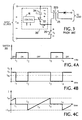
- oscillation in the reset circuit 30 may generally result in undesirable coupling of energy into the converter output in the form of noise at the frequency fr, or, as seen in Figures 5B to 5D, at a higher frequency associated with resonant ringing of the transformer leakage inductance (Ll, 123, Fig. 6) with both the reset capacitor 34 and the secondary capacitor 60 during the time period that the voltage Vc is positive.
- FIG. 7A Another characteristic of the circuit of Figure 3 is that the maximum allowable converter slew rate (e.g., the rate-of-change of duty cycle), and hence converter response time, are reduced as the value of Cr is increased.
- the damped reset circuit 230 is identical to the circuit of Figure 3 except that a passive damper, consisting of a damper resistor 39 and damper capacitor 35, has been connected across the reset capacitor 34.
- the damper resistor will dissipate energy at frequencies for which the impedance of Cd is low compared to Rd and for which the impedance of Cr is not low relative to Rd. Thus, at both very low and very high frequencies the damper creates little loss.
- waveforms are shown for the converter of Figure 6 with the undamped reset circuit 130 replaced with the damped reset circuit 230 of Figure 8.
- fr is chosen to be well below (e.g., approximately 10% of) the maximum operating frequency of the converter since this puts the "normal" operating frequency range of the converter well above fr and provides for minimum damper dissipation in this range.
- the characteristic frequency, fr, of a ZCS converter operating at frequencies up to 1 MHz would be set to be near 100 KHz. This provides effective damping with relatively little power loss at converter operating frequencies well above fr.
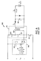
- Figure 10 shows a single-ended converter which includes an improved reset circuit 330.
- the reset switch 332 is opened when the primary switch is closed and vice versa.
- the improved reset circuit 330 differs from the circuits of Figures 3 and 8 by including a diode 350 connected across the reset capacitor 334. By poling the diode as shown, so that the reset capacitor can support positive values of the voltage Vc but cannot support negative values, the diode effectively prevents resonance (e.g., bidirectional energy transfer) from occurring between the reset capacitor 334 and the magnetizing inductance of the transformer 25.
- FIG. 11B show sustained oscillations, either at the characteristic frequency, fr, or at higher frequencies; the absence of the higher frequency oscillation is also an indicator that forward power flow from the reset circuit to the load has been eliminated.
- the decay in the current I in Figure 11B is due to the nonideal characteristics (e.g., parasitic resistances or finite voltage drops) of the diode 350, switch 332, and transformer primary winding 329 -- if all circuit elements were ideal, the current I would remain unchanged until the next operating cycle.
- the parasitic resistances of the reset switches 332, 32 is 0.1 ohm; the parasitic resistance of the transformer primary winding (e.g., primary winding 329 is 0.5 ohm; the diode 350, where used, is a silicon device).
- the average value of the capacitor voltage, Vc, in the circuit of Figure 10 will be approximately equal to Vin*D.
- the diode 350 will not become conductive and the waveforms for the reset circuit of Figure 10 will revert to those shown in Figure 4 for the prior art circuit of Figure 3.
- Preset represents the total amount of power dissipated in the reset circuit (e.g., circuits 230, 330) and Pd represents the loss in the "resonance-control" components used in the particular circuit (e.g., damper resistor 39 in circuit 230; diode 350 in circuit 330).
- loss in the passive damper circuit is strongly influenced by the values of Cr, Cd and Rd, and reductions in Cr result in lower values of Cd and increased amounts of Pd and Preset.
- the values of both Preset and Pd in the improved reset circuit 330 are seen to be much lower than the corresponding losses in the passively damped circuit 230, and the value of loss is only weakly a function of the value of Cr.
- a fundamental and important difference between the prior art reset circuit topology 30 of Figure 3 and the improved topology 330 of Figure 10 is that the average value of the current, I, in the prior art topology must be zero, whereas in the improved topology the average value of I can assume values which are nonzero and positive in the direction of the arrow. This is because all of the current, I, in the topology of Figure 3 must flow in the reset capacitor 34, and, as a result, the voltage Vc can only stabilize at an average value which is consistent with zero average flow of current I.
- the diode 350 provides a path for supporting a positive average value of I. This is how resonance is prevented.
- the improved reset circuit 330 may be placed across a transformer winding other than the primary winding 329.
- the circuit 330 is placed across the secondary winding 331 which delivers power to the load; in Figure 13B it is placed across an auxiliary winding 341.
- a benefit of "direct-coupled" reset e.g., as in Figure 10, where the reset circuit 330 is directly across the winding which is connected to the primary switch 20) is that the reset circuit 330 automatically acts as a snubber for the primary switch when the switch is turned off.
- a benefit of the use of an auxiliary winding 341 (Fig.
- a single reset circuit embodiment e.g., same value of reset capacitor, Cr; the same switch and diode
- a single reset circuit embodiment may be used within converters having widely varying values of both input and output voltage by simply adjusting the relative number of turns on the auxiliary winding to provide a predetermined value of transformer volts-per-turn.
- the reset circuit 330 is connected in other than a direct-coupled configuration, the ability of the circuit to snub the primary switch 20 will be diminished by the leakage inductances between the windings. In such cases care must be used to ensure that the coupling between windings is sufficiently high to prevent excessive voltage spikes on the switch 20.
- the reset switch 332 may, as shown in Figure 14, be embodied as a unipolar switch 339 (the direction of conduction of the current Isw being indicated by the arrow) in parallel with a diode 337. If, as shown in Figure 15A, the switch 332 is embodied as a MOSFET switching device 333, then the intrinsic body diode 337a of the MOSFET device 333 may, under appropriate circumstances, be exploited for use as the diode 337. Suitability of this approach will depend upon the reverse recovery characteristics of the intrinsic body diode (which, for a MOSFET switch, is a function of voltage rating) and the minimum required on-time of the reset switch during the converter operating cycle.
- the reverse recovery time of the intrinsic body diode of an International Rectifier IRFZ15 MOSFET, having a breakdown voltage rating of 60 Volts is 140 nanoseconds, maximum
- the reverse recovery time of the intrinsic body diode of an International Rectifier IRF710 MOSFET, having a breakdown voltage rating of 400 Volts is 520 nanoseconds, maximum.
- the relatively long recovery time of the intrinsic body diode in the cited higher voltage MOSFET would make it unsuitable for use as the diode 337 (Fig. 14) in applications in which the minimum on-time of the reset switch falls below 520 nanoseconds (e.g., in a ZCS converter with a maximum operating frequency around 1 MHz; in most PWM converters at high duty cycles).
- FIG. 15B shows a reset switch 332 embodiment using a MOSFET switch 333 and an external diode 342.
- a series diode 344 is put in series with the MOSFET switch 333.
- FIGS 16A to 16C Several embodiments of an improved reset circuit 330a, 330b, 330c are shown in Figures 16A to 16C, respectively.
- the improved reset circuit 330a incorporates the MOSFET switch 333 of Figure 15A into the circuit topology 330 of Figure 10; in Figure 16B the improved reset circuit 330b incorporates the MOSFET switch 333 and diodes 342, 344 of Figure 15B into the circuit topology 330 of Figure 10.
- the circuit of Figure 16B is modified by connecting the cathode of the reset diode 350 directly to the MOSFET switch 333, rather than to the series diode 344 as is done in Figure 16B. At times at which current is flowing in the reset diode 350, the circuit of Figure 16C will exhibit lower power loss than that of Figure 16B, since the current flow in the circuit of Figure 16C will bypass the series diode 344.
- the diode 344 (Fig. 15B, 16B, 16C) should be a device having a relatively low breakdown voltage rating (e.g., a Schottky diode having a low avalanche voltage rating, Vav).
- a relatively low breakdown voltage rating e.g., a Schottky diode having a low avalanche voltage rating, Vav.
- One reason for this is that diodes having lower breakdown voltages also have lower forward voltage drops and therefore will result in less circuit loss.
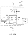
- Figures 17A and 17B show converter circuit models 10a, 10b which include, respectively, reset circuits 330a, 330c of the kind shown in Figures 16A and 16C, and inductances 127 which emulate the magnetizing inductance of a transformer.
- the drain-to-source capacitance, Cd 344, and the gate-to-drain capacitance, Cg 348, of the MOSFET 333 (the intrinsic body diode is not shown) and, in Figure 17B, the parasitic junction capacitance, Cj 346, of the external diode 342.
- Vin the converter input voltage
- Im magnetizing current
- the diode 344 has a low breakdown voltage (e.g., 20 Volts) then the diode 344 will avalanche when Im begins to flow in the reset circuit 330c and the capacitances 344, 348 will be discharged until the voltage across the MOSFET (e.g., the voltage across capacitor 344) falls below the breakdown voltage, Vav, of the diode 344, at which point the diode will come out of avalanche and cease conducting. Since Vav is much lower than Vin +Vc the amount of switching loss is substantially reduced. The same reasoning applies to the circuit embodiment of Figure 16B, which will also benefit from use of a series diode 344 having a low breakdown voltage rating.
- a low breakdown voltage e.g. 20 Volts
- the breakdown voltage rating, Vav, of the series diode 344 should not be made too low, however.
- Vs drain-source voltage
- Cd 344 equivalent gate-to-drain capacitance
- the flow of Ig can disrupt control circuitry 16 connected to the FET gate. By keeping Vav at a suitable value (e.g., 20 V) this problem can be avoided with minimal increase in switching losses.
- a suitable value e.g. 20 V
- the flow of Ig may be bypassed around the control circuitry 16 by adding a high-speed diode 347 (e.g., a Schottky diode) across the gate-to-source terminals of the MOSFET.
- Controlling the reset switch 332 (Fig. 10) in the improved reset circuit 330 is essentially the same as controlling the switch 32 in the prior art converter of Fig. 3.
- the reset switch 332 must be turned on after the primary switch 20 opens and must be off when the primary switch closes. If a reset switch of the kind shown in Figures 14 and 15 is used, the timing of the closure of the reset switch is not critical since the diode (337, Fig. 14) will begin to conduct magnetizing current Im as soon as the current commutates into the reset circuit 330.
- closure of the reset switch must not be allowed to occur while the primary switch is conductive as this can cause catastrophic failure of the converter. Therefore it is beneficial to provide means for sensing that the primary switch 20 has opened and enable closure of the reset switch only when this signal is present.
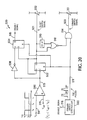
- Figures 18A and 18B Ways to sense the state of the primary switch are shown in Figures 18A and 18B.
- a reset circuit of the kind shown in Figure 16B is shown connected to a transformer 25 and a primary switch 20.
- a sense resistor 402 of a relatively small value Rs, is connected in series with the diode 342.
- the primary switch 20 opens and magnetizing current begins flowing, as a negative flow of the current I, in the diode 342 the voltage, Vm, across the resistor will go negative and this may be used to sense that the primary switch is no longer conductive.
- One drawback of the method of Figure 18A is that the use of the resistor will cause power loss.
- FIG. 18B A preferred method for sensing the state of the primary switch as a means of safely enabling the reset switch is shown in Figure 18B.
- a diode 410 a large value resistor 412 and bias source 414, of voltage Vb ⁇ Vin, are used as sensing elements.
- Vs a small voltage value
- the switch 333 begins to carry the current and the voltage Vs increases to a value Vk, which is more positive than Vz and approximately equal to the voltage drop across the switch, Vsw.
- Vk the voltage drop across the switch
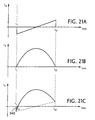
- the current which flows in the transformer primary, Ip will, as shown in Figures 21A through 21C, consist of a magnetizing current component, Im, and a forward current component, Io (e.g., in a ZCS converter, as shown in Fig. 21B, Io is the approximately sinusoidal portion of the transformer primary current which is reflected into the secondary winding).
- Io a forward current component
- the primary current, Ip is negative, and this flow of negative current will discharge the parasitic capacitance 343 of the primary switch 20 if the switch is off.
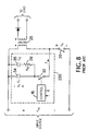
- FIG. 20 shows a reset switch controller 520 which incorporates some of the features described above.
- a primary switch controller 530 delivers Primary Switch Enable (MS) pulses 511 indicating when the primary switch 20 is to be turned on. Assuming that the reset switch 332 is turned on (e.g., the Reset Switch signal output of flip-flop 502 is high), delivery of a PSE pulse will cause both flip-flops 502, 504 to be reset via their reset inputs. This will cause the Reset Switch signal 501 to go low, initiating turn-off of the reset switch, and will also cause the Disable signal 515 to go high.
- MS Primary Switch Enable
- the Primary Switch Controller 530 will not deliver another PSE pulse unless the Disable signal 515 is low.
- the result is that the primary switch 20 is turned on a short time after the reset switch is turned off.
- the dead time is determined by circuit propagation times and the delay introduced by delay element 510 -- in a typical 1 Mhz ZCS converter the delay might be a few tens of nanoseconds. Provided that the delay is relatively short, its value is non-critical since the transformer magnetizing current which flows during the dead time will beneficially charge parasitic capacitances associated with both switches.
- This causes the output of the comparator 500 to go low, bringing the Disable signal low. This, in turn, signals the primary switch controller 530 that it is safe for it to deliver a subsequent PSE pulse 511. Some time later (e.g., at approximately time t tf) another PSE pulse is generated and the cycle is repeated.
- topologies and circuits described above may be adapted for use in other than single-ended converters (e.g.; full bridge or half-bridge converters).
Landscapes
- Engineering & Computer Science (AREA)
- Power Engineering (AREA)
- Dc-Dc Converters (AREA)
Claims (41)
- Dispositif destiné à être utilisé dans un convertisseur de puissance à commutation du type qui délivre une puissance depuis une source d'entrée DC dans une charge via un transformateur et qui a un commutateur primaire pour connecter ladite source DC à un enroulement primaire dudit transformateur pendant une partie de chaque cycle d'une succession de cycles de fonctionnement de convertisseur, le dispositif comportant un circuit de réinitialisation comportant : une branche de condensateur, un circuit série connecté entre ladite branche de condensateur et ledit transformateur, le dispositif étant caractérisé en ce que ledit circuit série comporte un circuit de commutation contrôlable et fournit le seul trajet pour achever un circuit comportant ladite branche de condensateur et ledit transformateur, ledit circuit de commutation contrôlable étant adapté pour permettre une circulation de courant entre ladite branche de condensateur et ledit transformateur à travers ledit circuit série pendant un état fermé et inhiber une circulation de courant entre ladite branche de condensateur et ledit transformateur à travers ledit circuit série pendant un état ouvert, et en ce qu'il comporte un circuit supplémentaire connecté à ladite branche de condensateur qui permet à un courant ayant une valeur moyenne non-nulle de circuler dans ledit circuit série et permet à l'énergie de magnétisation d'être transférée entre le transformateur et la branche de condensateur uniquement si la tension à travers la branche de condensateur est d'une polarité particulière, ledit circuit de réinitialisation étant efficace pour réinitialiser ledit transformateur en transférant l'énergie stockée dans ledit transformateur dans ladite branche de condensateur et en retour vers ledit transformateur sans renvoyer l'énergie dans ladite source d'entrée DC.
- Dispositif selon la revendication 1, caractérisé de plus en ce que le circuit de commutation entre dans lesdits états ouvert et fermé à des instants basés sur la commutation dudit commutateur primaire.
- Dispositif selon la revendication 1, caractérisé de plus en ce que le circuit de commutation est connecté en série à la branche de condensateur.
- Dispositif selon la revendication 1, caractérisé de plus en ce que le circuit supplémentaire comporte des éléments de circuit connectés pour inhiber une inversion de tension à travers ladite branche de condensateur.
- Convertisseur de puissance à commutation ayant un transformateur et un commutateur primaire pour connecter une source d'entrée DC et un enroulement primaire du transformateur pendant une partie de chaque cycle d'une succession de cycles de fonctionnement de convertisseur et comportant un dispositif selon l'une quelconque des revendications précédentes connecté à travers un enroulement du transformateur.
- Convertisseur de puissance à commutation selon la revendication 5, caractérisé de plus en ce que ledit enroulement comporte l'enroulement primaire.
- Convertisseur de puissance à commutation selon la revendication 5, caractérisé de plus en ce que ledit enroulement comporte un enroulement secondaire.
- Convertisseur de puissance à commutation selon la revendication 5, caractérisé de plus en ce que ledit enroulement comporte un enroulement auxiliaire.
- Dispositif selon la revendication 1, caractérisé de plus en ce que ledit circuit de commutation comporte un commutateur unidirectionnel connecté en parallèle à un élément de conduction unidirectionnel, ledit commutateur unidirectionnel et ledit élément de conduction unidirectionnel étant conçus pour établir une conduction dans des directions opposées.
- Dispositif selon la revendication 9, caractérisé de plus en ce que ledit commutateur unidirectionnel comporte un transistor MOSFET.
- Dispositif selon la revendication 9, caractérisé de plus en ce que ledit élément de conduction unidirectionnel comporte la diode de corps intrinsèque dudit transistor MOSFET.
- Dispositif selon la revendication 9, caractérisé de plus en ce que ledit commutateur unidirectionnel comporte un transistor MOSPET en série avec une diode série, ladite diode série et ledit transistor MOSFET étant polarisés pour établir une conduction dans la même direction.
- Dispositif selon la revendication 4, caractérisé de plus en ce que lesdits éléments de circuit comportent une diode de réinitialisation connectée en parallèle à ladite branche de condensateur.
- Dispositif selon la revendication 1, caractérisé de plus en ce que ladite polarité particulière est celle qui va avoir pour résultat une inversion de polarité du courant de magnétisation de transformateur pendant ledit état fermé.
- Dispositif selon la revendication 12, caractérisé de plus en ce que ledit circuit de réinitialisation inclut des éléments de circuit qui inhibent une inversion de tension à travers ladite branche de condensateur et en ce que lesdits éléments de circuit comportent une diode de réinitialisation connectée à travers un circuit série comportant ladite branche de condensateur et ladite diode série.
- Dispositif selon la revendication 1, caractérisé de plus en ce que ledit convertisseur de puissance à commutation comporte un convertisseur de puissance direct.
- Dispositif selon la revendication 1, caractérisé de plus en ce que ledit convertisseur de puissance à commutation comporte un convertisseur à commutation de courant nul.
- Dispositif selon la revendication 1, caractérisé de plus en ce que ledit convertisseur de puissance à commutation comporte un convertisseur PWM.
- Dispositif selon la revendication 1, caractérisé de plus en ce que ledit commutateur primaire permet une circulation de courant depuis ladite source d'entrée DC dans ledit enroulement primaire pendant un état fermé primaire et inhibe une circulation de courant depuis ladite source d'entrée DC dans ledit enroulement primaire pendant un état ouvert primaire, et en ce que ledit circuit de commutation est dans ledit état ouvert avant la période de temps où ledit commutateur primaire se trouve dans l'état fermé primaire.
- Dispositif selon la revendication 1, caractérisé de plus en ce que ledit commutateur primaire permet une circulation de courant depuis ladite source d'entrée DC dans ledit enroulement primaire pendant un état fermé primaire et inhibe une circulation de courant depuis ladite source d'entrée DC dans ledit enroulement primaire pendant un état ouvert primaire, et en ce que ledit circuit de commutation entre dans ledit état fermé pendant la période de temps où ledit commutateur primaire se trouve dans l'état ouvert primaire.
- Dispositif selon la revendication 1, caractérisé de plus en ce que ledit commutateur primaire permet une circulation de courant depuis ladite source d'entrée DC dans ledit enroulement primaire pendant un état fermé primaire et inhibe une circulation de courant depuis ladite source d'entrée DC dans ledit enroulement primaire pendant un état ouvert primaire, et en ce que ledit circuit de commutation reste dans ledit état ouvert tout au long de la période de temps où ledit commutateur primaire se trouve dans l'état fermé primaire.
- Dispositif selon la revendication 1, caractérisé de plus en ce qu'il comporte un circuit de commande de balayage pour inhiber l'initiation d'un cycle de fonctionnement de convertisseur sur la base de la valeur d'un courant de magnétisation dans ledit transformateur.
- Dispositif selon la revendication 1, caractérisé de plus en ce que ledit commutateur primaire permet à un courant de circuler depuis ladite source d'entrée DC dans ledit enroulement primaire essentiellement au même moment où ledit circuit de commutation entre dans ledit état ouvert.
- Dispositif selon la revendication 1, caractérisé de plus en ce que ledit commutateur primaire permet à un courant de circuler depuis ladite source d'entrée dans ledit enroulement primaire un retard fini de temps après que ledit circuit de commutation soit entré dans ledit état ouvert.
- Dispositif selon la revendication 24, caractérisé de plus en ce que ledit retard fini s'adapte au chargement et déchargement de capacités dans ledit convertisseur.
- Dispositif selon la revendication 25, caractérisé de plus en ce que lesdites capacités comportent des capacités parasites.
- Dispositif selon la revendication 25, caractérisé de plus en ce que lesdites capacités sont associées audit commutateur primaire.
- Dispositif selon la revendication 25, caractérisé de plus en ce que lesdites capacités sont associées audit circuit de commutation.
- Dispositif selon la revendication 25, caractérisé de plus en ce que lesdites capacités sont associées à des enroulements dudit transformateur.
- Dispositif destiné à être utilisé dans un convertisseur de puissance à commutation du type ayant un transformateur pour transférer de l'énergie depuis une source d'entrée DC dans une charge pendant une partie de transfert d'énergie direct d'une succession de cycles de fonctionnement de convertisseur et un commutateur primaire pour connecter ladite source d'entrée DC à un enroulement primaire dudit transformateur pendant lesdites parties de transfert d'énergie direct, le dispositif comportant un condensateur de réinitialisation et un circuit série connecté entre ledit condensateur de réinitialisation et ledit transformateur, ledit dispositif étant caractérisé en ce que ledit circuit série fournit le seul trajet pour achever un circuit comportant ledit condensateur de réinitialisation et ledit transformateur, en ce que ledit circuit série comporte un commutateur de réinitialisation contrôlable, et en ce que le circuit de réinitialisation est conçu pour coopérer avec ledit circuit série pour connecter et déconnecter ledit condensateur de réinitialisation d'une manière qui permet la réinitialisation d'un noyau du transformateur et permet à un courant ayant une valeur moyenne non-nulle de circuler dans ledit circuit série, ledit circuit de réinitialisation comportant une diode de réinitialisation connectée en parallèle audit condensateur de réinitialisation pour inhiber une inversion de polarité de la tension à travers ledit condensateur.
- Procédé de réinitialisation destiné à être utilisé dans un convertisseur de puissance à commutation du type ayant un transformateur, un enroulement primaire pour connecter une source d'entrée DC à un enroulement du transformateur pendant une partie de chaque cycle d'une succession de cycles de fonctionnement de convertisseur , un condensateur de réinitialisation, et un circuit série connecté entre ledit condensateur de réinitialisation et ledit transformateur, ledit circuit série fournissant le seul trajet pour achever un circuit comportant ledit condensateur de réinitialisation et ledit transformateur, ledit circuit série comportant un commutateur de réinitialisation contrôlable qui permet une circulation de courant entre ledit condensateur de réinitialisation et ledit transformateur à travers ledit circuit série dans un état fermé et inhibe une circulation de courant entre ledit condensateur de réinitialisation et un transformateur dans un état ouvert, le procédé comportant la connexion et la déconnexion dudit condensateur de réinitialisation d'une manière qui permet la réinitialisation dudit transformateur et qui permet à un courant ayant une valeur moyenne non-nulle de circuler dans ledit circuit série.
- Procédé selon la revendication 31, dans lequel ledit commutateur primaire permet une circulation de courant entre ladite source d'entrée DC et ledit enroulement primaire dans un état fermé primaire et ledit commutateur primaire entre dans ledit état fermé primaire essentiellement au même moment où ledit commutateur de réinitialisation entre dans ledit état ouvert.
- Procédé selon la revendication 31, dans lequel ledit commutateur primaire permet une circulation de courant entre ladite source d'entrée DC et ledit enroulement primaire dans un état fermé primaire et ledit commutateur primaire entre dans ledit état fermé primaire un retard fini de temps après que ledit commutateur de réinitialisation soit entré dans ledit état ouvert.
- Dispositif de convertisseur de puissance à commutation comportant : une source d'entrée DC, un transformateur ayant un enroulement primaire, un commutateur primaire pour connecter ladite source DC audit enroulement primaire pendant une partie de chaque cycle d'une succession de cycles de fonctionnement de convertisseur, un condensateur de réinitialisation, et un circuit série connecté entre ledit condensateur de réinitialisation et ledit transformateur, le dispositif étant caractérisé en ce que ledit circuit série comporte un commutateur de réinitialisation contrôlable et fournit le seul trajet pour achever un circuit comportant ledit condensateur de réinitialisation et ledit transformateur, et en ce que ledit circuit de réinitialisation est agencé, ledit circuit de réinitialisation comportant une diode de réinitialisation connectée en parallèle audit condensateur de réinitialisation pour inhiber une inversion de polarité de la tension à travers ledit condensateur, ledit circuit de réinitialisation coopérant avec ledit commutateur de réinitialisation pour connecter et déconnecter ledit condensateur de réinitialisation d'une manière qui permet une réinitialisation d'un noyau dudit transformateur et permet à un courant ayant une valeur moyenne non-nulle de circuler dans ledit circuit série.
- Procédé d'alimentation de puissance comportant les étapes consistant à : initier un transfert d'énergie depuis une source d'entrée DC dans une charge via un transformateur en connectant ladite source d'entrée DC à un enroulement dudit transformateur pendant une partie de transfert d'énergie direct de chaque cycle d'une succession de cycles de fonctionnement de convertisseur, réinitialiser ledit transformateur pendant chaque cycle desdits cycles de convertisseur en fournissant un transfert d'énergie entre ledit transformateur et un condensateur de réinitialisation pendant une seconde partie desdits cycles de fonctionnement de convertisseur de sorte que le flux dans le transformateur est inversé, ladite étape consistant à fournir un transfert d'énergie entre ledit transformateur et un condensateur de réinitialisation incluant la fermeture d'un commutateur de réinitialisation contrôlable, et la dérivation sélective dudit condensateur de réinitialisation pour empêcher une inversion de polarité de la tension à travers ledit condensateur de réinitialisation.
- Procédé selon la revendication 35, dans lequel l'initiation de ladite étape d'initiation d'un transfert d'énergie coïncide essentiellement avec l'achèvement de ladite étape précédente de réinitialisation dudit transformateur.
- Procédé selon la revendication 35, comportant de plus l'étape consistant à imposer un retard fini de temps après avoir effectuer ladite étape de réinitialisation dudit transformateur et avant de commencer ladite étape d'initiation de transfert d'énergie.
- Procédé selon la revendication 33 ou 37, dans lequel ledit retard fini s'adapte à un chargement et un déchargement de capacités.
- Procédé selon la revendication 38, dans lequel lesdites capacités comportent des capacités parasites.
- Procédé selon la revendication 39, dans lequel lesdites capacités sont associées à au moins un commutateur.
- Procédé selon la revendication 39, dans lequel lesdites capacités sont associées à au moins un enroulement dudit transformateur.
Priority Applications (1)
| Application Number | Priority Date | Filing Date | Title |
|---|---|---|---|
| EP02078757A EP1278295A3 (fr) | 1995-01-17 | 1996-01-09 | Contrôle de l'énérgie magnétique stockée dans les transformateurs des convertisseurs de puissance |
Applications Claiming Priority (2)
| Application Number | Priority Date | Filing Date | Title |
|---|---|---|---|
| US37311295A | 1995-01-17 | 1995-01-17 | |
| US373112 | 1999-08-11 |
Related Child Applications (1)
| Application Number | Title | Priority Date | Filing Date |
|---|---|---|---|
| EP02078757A Division EP1278295A3 (fr) | 1995-01-17 | 1996-01-09 | Contrôle de l'énérgie magnétique stockée dans les transformateurs des convertisseurs de puissance |
Publications (3)
| Publication Number | Publication Date |
|---|---|
| EP0723331A2 EP0723331A2 (fr) | 1996-07-24 |
| EP0723331A3 EP0723331A3 (fr) | 1997-04-23 |
| EP0723331B1 true EP0723331B1 (fr) | 2003-05-07 |
Family
ID=23471012
Family Applications (2)
| Application Number | Title | Priority Date | Filing Date |
|---|---|---|---|
| EP96300150A Expired - Lifetime EP0723331B1 (fr) | 1995-01-17 | 1996-01-09 | Contrôle de l'énergie magnétique stockée dans les transformateurs des convertisseurs de puissance |
| EP02078757A Withdrawn EP1278295A3 (fr) | 1995-01-17 | 1996-01-09 | Contrôle de l'énérgie magnétique stockée dans les transformateurs des convertisseurs de puissance |
Family Applications After (1)
| Application Number | Title | Priority Date | Filing Date |
|---|---|---|---|
| EP02078757A Withdrawn EP1278295A3 (fr) | 1995-01-17 | 1996-01-09 | Contrôle de l'énérgie magnétique stockée dans les transformateurs des convertisseurs de puissance |
Country Status (4)
| Country | Link |
|---|---|
| US (2) | US5805434A (fr) |
| EP (2) | EP0723331B1 (fr) |
| JP (1) | JP2781768B2 (fr) |
| DE (1) | DE69627909T2 (fr) |
Families Citing this family (43)
| Publication number | Priority date | Publication date | Assignee | Title |
|---|---|---|---|---|
| JPH1141927A (ja) * | 1997-07-16 | 1999-02-12 | Fujitsu Ltd | Dc/dcコンバータ |
| US6110213A (en) | 1997-11-06 | 2000-08-29 | Vlt Coporation | Fabrication rules based automated design and manufacturing system and method |
| FR2773013B1 (fr) * | 1997-12-23 | 2000-03-03 | Sextant Avionique | Procede de commande d'un convertisseur de tension continu-continu a stockage inductif |
| AU7093900A (en) * | 1999-09-03 | 2001-04-10 | Lambda Electronics | Inductor current sensing |
| US6282107B1 (en) * | 2000-03-07 | 2001-08-28 | Vlt Corporation | Integrated sense and switch circuitry for transformer core resetting |
| US6658051B1 (en) * | 2000-10-31 | 2003-12-02 | Centillium Communications, Inc. | Electrical isolation techniques for DSL modem |
| SE520159C2 (sv) * | 2001-01-26 | 2003-06-03 | Ericsson Telefon Ab L M | Anordning för avmagnetisering av en transformator |
| US6496392B2 (en) * | 2001-04-13 | 2002-12-17 | Power Integrations, Inc. | Dissipative clamping of an electrical circuit with a clamp voltage varied in response to an input voltage |
| JP3528921B2 (ja) * | 2001-08-29 | 2004-05-24 | サンケン電気株式会社 | スイッチング電源装置 |
| JP3839737B2 (ja) * | 2002-03-01 | 2006-11-01 | 株式会社小糸製作所 | 直流電圧変換回路 |
| EP1495532B1 (fr) * | 2002-04-12 | 2014-09-24 | DET International Holding Limited | Convertisseur a commutation souple mettant en oeuvre une correction de courant |
| AU2003283764A1 (en) * | 2003-01-14 | 2004-08-10 | Koninklijke Philips Electronics N.V. | Circuit and method for providing power to a load, especially a high-intensity discharge lamp |
| DE102004033994B4 (de) * | 2003-07-16 | 2017-07-27 | Denso Corporation | Gleichstrom-Gleichstrom-Wandler |
| FR2861916A1 (fr) * | 2003-10-31 | 2005-05-06 | St Microelectronics Sa | Commande d'un transistor mos en element de redressement |
| TWI265670B (en) * | 2004-02-20 | 2006-11-01 | Skynet Electronic Co Ltd | Flyback converter capable of performing a zero voltage switch in boundary mode |
| US7230838B2 (en) * | 2004-12-28 | 2007-06-12 | Monolithic Power Systems, Inc. | Active damping control for a switch mode power supply |
| US8036539B2 (en) * | 2005-06-28 | 2011-10-11 | Finisar Corporation | Gigabit ethernet longwave optical transceiver module having amplified bias current |
| JP4739059B2 (ja) * | 2006-02-23 | 2011-08-03 | ルネサスエレクトロニクス株式会社 | Dc/dcコンバータ用半導体装置 |
| KR101165386B1 (ko) | 2006-06-13 | 2012-07-12 | 페어차일드코리아반도체 주식회사 | 준공진형 컨버터 및 그 제어 방법 |
| KR101370650B1 (ko) | 2007-04-25 | 2014-03-10 | 페어차일드코리아반도체 주식회사 | 스위치 제어 장치, 스위치 제어 방법 및 이를 이용하는컨버터 및 그 구동방법 |
| GB2448758A (en) * | 2007-04-27 | 2008-10-29 | Cambridge Semiconductor Ltd | A switching power converter with reduced collector dv/dt |
| KR101129391B1 (ko) | 2007-08-13 | 2012-03-28 | 삼성전자주식회사 | 수동 클램프 회로를 갖는 스위칭 모드 전원공급장치 |
| JP5157987B2 (ja) * | 2009-03-25 | 2013-03-06 | 株式会社豊田自動織機 | 絶縁形dc−dcコンバータ |
| EP2244383A1 (fr) * | 2009-04-23 | 2010-10-27 | Mitsubishi Electric R&D Centre Europe B.V. | Procédé et appareil pour le contrôle du fonctionnement d'un circuit d'amortissement |
| US8385087B2 (en) * | 2009-09-17 | 2013-02-26 | Linear Technology Corporation | Extending achievable duty cycle range in DC/DC forward converter with active clamp reset |
| TWI389438B (zh) * | 2009-11-02 | 2013-03-11 | Analog Integrations Corp | 高轉換效率之電壓轉換器 |
| US8139379B2 (en) * | 2010-02-17 | 2012-03-20 | Fsp Technology Inc. | Reverse energy recovery circuit |
| US8743523B2 (en) | 2010-07-28 | 2014-06-03 | General Electric Company | Systems, methods, and apparatus for limiting voltage across a switch |
| US9112498B2 (en) * | 2011-11-01 | 2015-08-18 | Dialog Semiconductor Inc. | Dynamic MOSFET gate drivers |
| US8982584B2 (en) | 2011-11-15 | 2015-03-17 | Dialog Semiconductor Inc. | Power supply regulation for ultra-low load and no-load operation |
| US8964422B2 (en) | 2011-11-16 | 2015-02-24 | Dialog Semiconductor Inc. | EMI frequency spreading method for switching power converter |
| JP6224994B2 (ja) * | 2013-11-01 | 2017-11-01 | キヤノン株式会社 | 情報処理装置およびその制御方法 |
| US9973098B2 (en) * | 2015-08-19 | 2018-05-15 | Astec International Limited | Fixed frequency discontinuous conduction mode flyback power converters employing zero voltage switching |
| US10141853B2 (en) * | 2017-02-09 | 2018-11-27 | Delta Electronics, Inc. | Power converter and method of control thereof |
| US10333418B2 (en) * | 2017-04-10 | 2019-06-25 | Delta Electronics (Shanghai) Co., Ltd | Control device and control method |
| US20190036459A1 (en) * | 2017-04-28 | 2019-01-31 | Astec International Limited | Flyback power converters including adaptive clamp circuits for adjusting resonant frequencies |
| US10418912B2 (en) | 2017-12-21 | 2019-09-17 | Silanna Asia Pte Ltd | Power converter with active clamp |
| US10707766B2 (en) | 2018-02-02 | 2020-07-07 | Silanna Asia Pte Ltd | Integrated self-driven active clamp |
| US10461626B1 (en) | 2019-01-14 | 2019-10-29 | Silanna Asia Pte Ltd | Active clamp circuit |
| TWI709291B (zh) * | 2019-04-26 | 2020-11-01 | 全漢企業股份有限公司 | 電源轉換器及其控制電路 |
| US10673342B1 (en) | 2019-05-02 | 2020-06-02 | Silanna Asia Pte Ltd | Active clamping with bootstrap circuit |
| US11411510B2 (en) * | 2020-01-24 | 2022-08-09 | Lear Corporation | DC/AC inverter resonance topology |
| CN113852272B (zh) | 2020-06-26 | 2024-09-13 | 马克西姆综合产品公司 | 通量校正开关电源转换器 |
Family Cites Families (63)
| Publication number | Priority date | Publication date | Assignee | Title |
|---|---|---|---|---|
| US1672215A (en) | 1923-08-15 | 1928-06-05 | Western Electric Co | Wave varying and transmitting |
| US3311805A (en) | 1964-11-02 | 1967-03-28 | Kittl Emil | Asymmetrical low voltage converter |
| FR96147E (fr) | 1967-09-14 | 1972-05-19 | Ibm | Convertisseur améliore de courant continu en courant continu avec alimentation constante vers la charge. |
| US3538353A (en) | 1967-10-13 | 1970-11-03 | Gen Electric | Switching circuit |
| US3490027A (en) | 1967-12-05 | 1970-01-13 | Ibm | Transistor converter amplifier circuit |
| SE377988B (fr) | 1968-10-16 | 1975-08-04 | P E K Udden | |
| NL7309056A (fr) | 1973-06-29 | 1974-12-31 | ||
| US4063306A (en) | 1976-09-24 | 1977-12-13 | General Electric Company | Actively switched damping circuit |
| US4168477A (en) | 1978-02-21 | 1979-09-18 | Gould Advance Limited | Electric regulators |
| US4186434A (en) | 1978-03-23 | 1980-01-29 | The United States Of America As Represented By The Secretary Of The Army | Means for producing and controlling dead-time of the switching transistors DC-to-DC and DC-to-AC converters |
| US4178628A (en) | 1978-05-12 | 1979-12-11 | R & I Patent Corporation | Switching type regulated power supply |
| JPS5840913B2 (ja) | 1978-11-16 | 1983-09-08 | 横河電機株式会社 | 一般化dc/dcコンバ−タ |
| GB2050081B (en) * | 1979-03-15 | 1982-12-08 | Tokyo Shibaura Electric Co | High frequency switching regulator circuit |
| JPS5826381B2 (ja) * | 1979-04-28 | 1983-06-02 | 信越ポリマ−株式会社 | 電磁気シ−ルドガスケットおよびその製造方法 |
| JPS5911257B2 (ja) | 1979-12-19 | 1984-03-14 | 恒男 池上 | Dc−dcコンバ−タ |
| US4300191A (en) | 1980-01-31 | 1981-11-10 | Powercube Corporation | Pulse width modulated current fed inverter power supply |
| JPS605144B2 (ja) | 1980-04-01 | 1985-02-08 | 日本電信電話株式会社 | 電力転送装置 |
| SU892614A1 (ru) | 1980-04-11 | 1981-12-23 | Московский Ордена Ленина Энергетический Институт | Однотактный регул тор посто нного напр жени |
| US4347474A (en) | 1980-09-18 | 1982-08-31 | The United States Of America As Represented By The Secretary Of The Navy | Solid state regulated power transformer with waveform conditioning capability |
| SU959234A1 (ru) | 1981-02-27 | 1982-09-15 | Московский Ордена Ленина Энергетический Институт | Устройство дл регулировани напр жени |
| US4415959A (en) | 1981-03-20 | 1983-11-15 | Vicor Corporation | Forward converter switching at zero current |
| SU1003067A1 (ru) | 1981-04-01 | 1983-03-07 | Московский Ордена Ленина И Ордена Октябрьской Революции Энергетический Институт | Однотактный регул тор посто нного напр жени |
| GB2097606B (en) | 1981-04-23 | 1984-04-18 | Standard Telephones Cables Ltd | Dc to dc converter |
| SU989552A1 (ru) | 1981-07-13 | 1983-01-15 | Московский Ордена Ленина И Ордена Октябрьской Революции Энергетический Институт | Стабилизированный однотактный преобразователь |
| US4441146A (en) * | 1982-02-04 | 1984-04-03 | Vicor Corporation | Optimal resetting of the transformer's core in single ended forward converters |
| SU1107233A1 (ru) | 1983-01-03 | 1984-08-07 | Московский Ордена Ленина И Ордена Октябрьской Революции Энергетический Институт | Преобразователь посто нного напр жени |
| SU1136275A1 (ru) | 1983-01-07 | 1985-01-23 | Московский Ордена Ленина И Ордена Октябрьской Революции Энергетический Институт | Импульсный регул тор посто нного напр жени |
| US4607323A (en) | 1984-04-17 | 1986-08-19 | Sokal Nathan O | Class E high-frequency high-efficiency dc/dc power converter |
| SU1224921A1 (ru) | 1984-06-11 | 1986-04-15 | Московский Ордена Ленина И Ордена Октябрьской Революции Энергетический Институт | Преобразователь посто нного напр жени в посто нное |
| US4611267A (en) * | 1985-02-25 | 1986-09-09 | General Electric Company | Snubber arrangements with energy recovery for power converters using self-extinguishing devices |
| DE3616160A1 (de) * | 1986-05-14 | 1987-11-19 | Deutsche Automobilgesellsch | Dc/dc-eintaktdurchflusswandler |
| SU1367112A1 (ru) | 1986-07-25 | 1988-01-15 | Московский энергетический институт | Преобразователь посто нного напр жени в посто нное |
| US4928200A (en) | 1987-04-02 | 1990-05-22 | Cherry Semiconductor Corporation | Overcurrent protection for switching mode power converter |
| US4788634A (en) * | 1987-06-22 | 1988-11-29 | Massachusetts Institute Of Technology | Resonant forward converter |
| US4857822A (en) | 1987-09-23 | 1989-08-15 | Virginia Tech Intellectual Properties, Inc. | Zero-voltage-switched multi-resonant converters including the buck and forward type |
| US4809148A (en) | 1987-10-21 | 1989-02-28 | British Columbia Telephone Company | Full-fluxed, single-ended DC converter |
| US4870554A (en) * | 1987-11-12 | 1989-09-26 | Power Systems, Inc. | Active snubber forward converter |
| GB8816282D0 (en) * | 1988-07-08 | 1988-08-10 | Ogeden K | H f switch inductor power supply |
| US4931716A (en) | 1989-05-05 | 1990-06-05 | Milan Jovanovic | Constant frequency zero-voltage-switching multi-resonant converter |
| US5019957A (en) * | 1989-07-24 | 1991-05-28 | Wilkinson Bruce L | Forward converter type of switched power supply |
| US4975821A (en) * | 1989-10-10 | 1990-12-04 | Lethellier Patrice R | High frequency switched mode resonant commutation power supply |
| JPH0748944B2 (ja) * | 1989-10-14 | 1995-05-24 | 東光株式会社 | Dc―dcコンバータ |
| US4959764A (en) | 1989-11-14 | 1990-09-25 | Computer Products, Inc. | DC/DC converter switching at zero voltage |
| US5038264A (en) * | 1990-06-11 | 1991-08-06 | General Electric Company | Multiple-output, single-ended, resonant power converter |
| US5126931A (en) | 1990-09-07 | 1992-06-30 | Itt Corporation | Fixed frequency single ended forward converter switching at zero voltage |
| US5173846A (en) | 1991-03-13 | 1992-12-22 | Astec International Ltd. | Zero voltage switching power converter |
| US5291382A (en) | 1991-04-10 | 1994-03-01 | Lambda Electronics Inc. | Pulse width modulated DC/DC converter with reduced ripple current coponent stress and zero voltage switching capability |
| DE4121942A1 (de) * | 1991-07-03 | 1993-01-07 | Ant Nachrichtentech | Resonanzwandler |
| US5374857A (en) | 1992-05-29 | 1994-12-20 | Sgs-Thomson Microelectronics, Inc. | Circuit for providing drive current to a motor using a sensefet current sensing device and a fast amplifier |
| US5282123A (en) * | 1992-12-16 | 1994-01-25 | At&T Bell Laboratories | Clamped mode DC-DC converter |
| US5434768A (en) * | 1993-02-12 | 1995-07-18 | Rompower | Fixed frequency converter switching at zero voltage |
| US5303138A (en) | 1993-04-29 | 1994-04-12 | At&T Bell Laboratories | Low loss synchronous rectifier for application to clamped-mode power converters |
| EP0627810B1 (fr) * | 1993-05-31 | 1996-12-18 | STMicroelectronics S.r.l. | Régulateur à temps de montée de puissance à extinction en demi-pont utilisant un condensateur unique |
| US5424933A (en) * | 1994-01-03 | 1995-06-13 | Avionic Instruments, Inc. | Resonant forward converter circuit with control circuit for controlling switching transistor on and off times |
| US5486752A (en) * | 1994-06-17 | 1996-01-23 | Center For Innovative Technology** | Zero-current transition PWM converters |
| US5774350A (en) | 1995-04-07 | 1998-06-30 | Sgs-Thomson Microelectronics S.A. | Integrated low dissipation power controller |
| JP2795217B2 (ja) | 1995-06-01 | 1998-09-10 | 日本電気株式会社 | 同期整流方式コンバータ |
| US5973939A (en) | 1996-08-29 | 1999-10-26 | Trw Inc. | Double forward converter with soft-PWM switching |
| US5814884C1 (en) | 1996-10-24 | 2002-01-29 | Int Rectifier Corp | Commonly housed diverse semiconductor die |
| US5886383A (en) | 1997-01-10 | 1999-03-23 | International Rectifier Corporation | Integrated schottky diode and mosgated device |
| US6121545A (en) * | 1997-07-11 | 2000-09-19 | Parker-Hannifin Corporation | Low closure force EMI shielding spacer gasket |
| US5812383A (en) | 1997-07-31 | 1998-09-22 | Philips Electronics North North America Corporation | Low power stand-by for switched-mode power supply circuit with burst mode operation |
| CA2318433A1 (fr) * | 1998-02-17 | 1999-08-19 | Parker-Hannifin Corporation | Panneau de ventilation blinde contre les interferences electromagnetiques et procede associe |
-
1996
- 1996-01-09 DE DE69627909T patent/DE69627909T2/de not_active Expired - Fee Related
- 1996-01-09 EP EP96300150A patent/EP0723331B1/fr not_active Expired - Lifetime
- 1996-01-09 EP EP02078757A patent/EP1278295A3/fr not_active Withdrawn
- 1996-01-17 JP JP8005954A patent/JP2781768B2/ja not_active Expired - Fee Related
-
1997
- 1997-05-23 US US08/862,528 patent/US5805434A/en not_active Ceased
-
2000
- 2000-09-08 US US09/657,970 patent/USRE38196E1/en not_active Expired - Lifetime
Also Published As
| Publication number | Publication date |
|---|---|
| DE69627909D1 (de) | 2003-06-12 |
| EP0723331A3 (fr) | 1997-04-23 |
| EP1278295A2 (fr) | 2003-01-22 |
| US5805434A (en) | 1998-09-08 |
| EP1278295A3 (fr) | 2004-12-29 |
| JP2781768B2 (ja) | 1998-07-30 |
| DE69627909T2 (de) | 2003-11-13 |
| EP0723331A2 (fr) | 1996-07-24 |
| JPH0937548A (ja) | 1997-02-07 |
| USRE38196E1 (en) | 2003-07-22 |
Similar Documents
| Publication | Publication Date | Title |
|---|---|---|
| EP0723331B1 (fr) | Contrôle de l'énergie magnétique stockée dans les transformateurs des convertisseurs de puissance | |
| US5636114A (en) | Lossless snubber circuit for use in power converters | |
| US5430633A (en) | Multi-resonant clamped flyback converter | |
| US5539630A (en) | Soft-switching converter DC-to-DC isolated with voltage bidirectional switches on the secondary side of an isolation transformer | |
| US6788555B2 (en) | Regulation of bi-directional flyback converter | |
| US8054655B2 (en) | Tail current control of isolated converter and apparatus thereof | |
| US5126931A (en) | Fixed frequency single ended forward converter switching at zero voltage | |
| Noon | UC3855A/B high performance power factor preregulator | |
| US9716437B2 (en) | Power converter for a switching power supply and manner of operation thereof | |
| US7859859B2 (en) | Primary side sampled feedback control in power converters | |
| KR100411327B1 (ko) | 다중 전압 출력을 갖는 전원 장치를 구비하는 다중 모드모니터 | |
| Andreycak | Zero voltage switching resonant power conversion | |
| JPH0247196B2 (fr) | ||
| US11451152B2 (en) | Active clamp circuit with steering network | |
| JPH09103070A (ja) | ゼロ電流スイッチングパワーコンバータ | |
| US12062989B2 (en) | Power converter and controller for a power converter and manners of operation thereof | |
| US20040145273A1 (en) | Electronic driver circuit for high-speed actuation of high-capacitance actuators | |
| US5977754A (en) | Offset resonance zero volt switching boost converter | |
| JP2769451B2 (ja) | 量子化電力変換装置 | |
| WO2001018946A1 (fr) | Detection de courant inductif | |
| US12009754B2 (en) | Switching power converter with reduced voltage switching of the primary switch | |
| JP3610383B2 (ja) | フライバック形コンバータ | |
| US20250088118A1 (en) | Switch mode power converter with adaptive gate voltage regulation for fast turn-off of synchronous rectifier | |
| TW202527451A (zh) | 用於控制諧振電源轉換器之轉換控制電路及其控制方法 | |
| JP2024543662A (ja) | 共振網用デュアルパスアクティブダンパー |
Legal Events
| Date | Code | Title | Description |
|---|---|---|---|
| PUAI | Public reference made under article 153(3) epc to a published international application that has entered the european phase |
Free format text: ORIGINAL CODE: 0009012 |
|
| AK | Designated contracting states |
Kind code of ref document: A2 Designated state(s): DE FR GB |
|
| PUAL | Search report despatched |
Free format text: ORIGINAL CODE: 0009013 |
|
| AK | Designated contracting states |
Kind code of ref document: A3 Designated state(s): DE FR GB |
|
| 17P | Request for examination filed |
Effective date: 19970825 |
|
| 17Q | First examination report despatched |
Effective date: 19990407 |
|
| GRAG | Despatch of communication of intention to grant |
Free format text: ORIGINAL CODE: EPIDOS AGRA |
|
| GRAG | Despatch of communication of intention to grant |
Free format text: ORIGINAL CODE: EPIDOS AGRA |
|
| GRAG | Despatch of communication of intention to grant |
Free format text: ORIGINAL CODE: EPIDOS AGRA |
|
| GRAH | Despatch of communication of intention to grant a patent |
Free format text: ORIGINAL CODE: EPIDOS IGRA |
|
| GRAH | Despatch of communication of intention to grant a patent |
Free format text: ORIGINAL CODE: EPIDOS IGRA |
|
| GRAA | (expected) grant |
Free format text: ORIGINAL CODE: 0009210 |
|
| AK | Designated contracting states |
Designated state(s): DE FR GB |
|
| REG | Reference to a national code |
Ref country code: GB Ref legal event code: FG4D |
|
| REF | Corresponds to: |
Ref document number: 69627909 Country of ref document: DE Date of ref document: 20030612 Kind code of ref document: P |
|
| ET | Fr: translation filed | ||
| PLBE | No opposition filed within time limit |
Free format text: ORIGINAL CODE: 0009261 |
|
| STAA | Information on the status of an ep patent application or granted ep patent |
Free format text: STATUS: NO OPPOSITION FILED WITHIN TIME LIMIT |
|
| 26N | No opposition filed |
Effective date: 20040210 |
|
| PGFP | Annual fee paid to national office [announced via postgrant information from national office to epo] |
Ref country code: GB Payment date: 20050105 Year of fee payment: 10 |
|
| PGFP | Annual fee paid to national office [announced via postgrant information from national office to epo] |
Ref country code: FR Payment date: 20050117 Year of fee payment: 10 |
|
| PGFP | Annual fee paid to national office [announced via postgrant information from national office to epo] |
Ref country code: DE Payment date: 20050228 Year of fee payment: 10 |
|
| PG25 | Lapsed in a contracting state [announced via postgrant information from national office to epo] |
Ref country code: GB Free format text: LAPSE BECAUSE OF NON-PAYMENT OF DUE FEES Effective date: 20060109 |
|
| PG25 | Lapsed in a contracting state [announced via postgrant information from national office to epo] |
Ref country code: FR Free format text: LAPSE BECAUSE OF NON-PAYMENT OF DUE FEES Effective date: 20060131 |
|
| PG25 | Lapsed in a contracting state [announced via postgrant information from national office to epo] |
Ref country code: DE Free format text: LAPSE BECAUSE OF NON-PAYMENT OF DUE FEES Effective date: 20060801 |
|
| GBPC | Gb: european patent ceased through non-payment of renewal fee |
Effective date: 20060109 |
|
| REG | Reference to a national code |
Ref country code: FR Ref legal event code: ST Effective date: 20060929 |