EP0716550A2 - Schwingungssignalgeneratoranordnung - Google Patents
Schwingungssignalgeneratoranordnung Download PDFInfo
- Publication number
- EP0716550A2 EP0716550A2 EP95308459A EP95308459A EP0716550A2 EP 0716550 A2 EP0716550 A2 EP 0716550A2 EP 95308459 A EP95308459 A EP 95308459A EP 95308459 A EP95308459 A EP 95308459A EP 0716550 A2 EP0716550 A2 EP 0716550A2
- Authority
- EP
- European Patent Office
- Prior art keywords
- value
- signal
- video signals
- phase
- accumulator
- Prior art date
- Legal status (The legal status is an assumption and is not a legal conclusion. Google has not performed a legal analysis and makes no representation as to the accuracy of the status listed.)
- Granted
Links
Images


Classifications
-
- H—ELECTRICITY
- H04—ELECTRIC COMMUNICATION TECHNIQUE
- H04N—PICTORIAL COMMUNICATION, e.g. TELEVISION
- H04N9/00—Details of colour television systems
- H04N9/44—Colour synchronisation
- H04N9/45—Generation or recovery of colour sub-carriers
Definitions
- the present invention relates to oscillatory signal generator arrangements, and particularly to such arrangements for generating colour subcarrier signals for use with digitally generated or computer generated video signals.
- a digital phase locked loop which is arranged to be clocked by clock pulses locked in frequency to the line frequency of said incoming video signals comprises a digital accumulator, means to add an incremental digital value to the count registered by said accumulator in response to each clock pulse such that said count follows a periodic sawtooth waveform with a period, determined by the maximum count value of said accumulator and by said incremental digital value, defining the period of said colour subcarrier signal, phase comparator means to compare the phase of said periodic sawtooth waveform with the phase of a reference waveform derived from said incoming video signals, and means to determine the value of said incremental digital value in dependence upon an output signal of said phase comparator means.
- said incremental digital value is the sum of a seed value, a value proportional to the instantaneous value of the output signal of said phase comparator and a value proportional to the integral of the output signal of said phase comparator.
- the phase comparator may comprise a two-input exclusive-OR gating means to one input of which are applied binary values dependent upon the instantaneous value of said reference waveform on the occurrence of said clock pulses and to the other input of which are applied binary values dependent upon the most-significant-bit state of said accumulator.
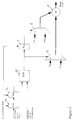
- an arrangement for genlocking digitally generated video signals to incoming video signals, on an input 1, derived from a video cassette recorder (VCR) or from a cable or broadcast television system (not shown), so that the images represented by the digitally generated video signals may be displayed with or overlaid on the VCR or television images, comprises a digital phase-locked-loop signal generator 2.
- This signal generator 2 comprises a digital accumulator 3, a digital phase detector or comparator 4, an integrating up/down counter 5, gain units 6 and 7 and summing circuits 8 and 9.
- the generator 2 operates under the control of clock pulses from a line-locked clock generator 10, at a nominal frequency of, say, 27 MHz, such that an incremental digital value, consisting of a'seed' value entered at the summing circuit 8 plus or minus contributions by way of the gain units 6 and 7 which depend in value upon the output of the phase comparator 4, is added on the occurrence of each clock pulse to the count state registered by the accumulator 3.
- This count state therefore increases in a series of steps until an overflow occurs, whereupon the increase begins again from the remainder count state.
- a periodic output signal may then be derived from, say, the count state of the two most significant bit stages of the accumulator 3. For an output signal having a periodicity or frequency of the order of 3.5 MHz each cycle of the accumulator count state will be completed in some seven or eight steps at the clock rate of 27MHz.
- the periodic output signal from the accumulator 3, with a 90° phase offset added in a summing circuit 11, is applied as a two-state signal to one input of the phase comparator 4, to the other input of which is applied a reference square wave signal derived in a phase-locked loop circuit 12 from the colour burst of the incoming video signals on the input 1.
- the reference square wave signal is clocked through register stages 13 and 14 to one input of an exclusive -OR gate 15, the periodic output signal from the summing circuit 11 being applied to the other input of this gate.
- the output of the exclusive-OR gate 15 is applied to a multiplexer or selector stage 16 and to a register stage 17, the output of which in turn is applied to a selector circuit 18. Outputs from the two selector stages are combined in a summing circuit 19 to provide the output of the phase comparator 4.
- the reference square wave 20, Figure 3(a) is effectively retimed by the line locked clock pulses, Figure 3(b), to produce a slightly delayed waveform Figure 3(d), the output of the summing circuit 11 being shown as Figure 3(c).
- the output of the exclusive-OR gate 15 is a two-state signal which in dependence upon its value, 0 or 1, on the occurrence of a clock pulse contributes a value of -1 or +1 respectively to the summing circuit 19.
- the output signal of the register stage 17,in dependence upon whether its value is 0 or 1, contributes a value of -16 or +16 to the summing circuit 19.
- These values may for example be represented in twos-complement arithmetical form.
- the inverse of the retimed reference square wave, shown as Figure 3(e), is the waveform which is compared with the waveform of Figure 3(c), producing an output signal value from the summing circuit 19, Figure 3(f), which varies between -17 and +17.
- the output signal values from the comparator 4 are applied to the integrator 5, which may for example be a fourteen-bit integrator, supporting an integral of the phase error value of between -8192 and +8191.
- the value represented by the states of the three most significant bit stages of the integrator 5 is applied by way of gain unit 7, which multiplies that value by a predetermined power of two, to the summing citcuit 9.
- the output signal values from the comparator 4 are mulitplied by a power of two in the gain unit 6 and the result added to the seed value in the summing circuit 8.
- the total value at the output of the summing circuit 9 finally is applied, at each clock pulse, as the incremental value to step the accumulator 3.
- ROM read-only memory
- any short term and long term variations respectively in the frequency of the line-locked clock will be countered, such that, say, if the clock frequency increases a smaller mean value will be applied to the input of accumulator 3 and vice versa.
- Values of n may be from 12 to 26, experiments indicating that for values below 12 the quality of lock deteriorates markedly.
- the factors G1 and G2 are set to zero and a value of n of at least 24 is used.
Landscapes
- Engineering & Computer Science (AREA)
- Multimedia (AREA)
- Signal Processing (AREA)
- Processing Of Color Television Signals (AREA)
- Electrophonic Musical Instruments (AREA)
- Slot Machines And Peripheral Devices (AREA)
- Investigating Or Analyzing Materials By The Use Of Ultrasonic Waves (AREA)
- Apparatuses For Generation Of Mechanical Vibrations (AREA)
- Stabilization Of Oscillater, Synchronisation, Frequency Synthesizers (AREA)
Applications Claiming Priority (2)
| Application Number | Priority Date | Filing Date | Title |
|---|---|---|---|
| GB9424839 | 1994-12-09 | ||
| GB9424839A GB2295935B (en) | 1994-12-09 | 1994-12-09 | Oscillatory signal generator arrangement |
Publications (3)
| Publication Number | Publication Date |
|---|---|
| EP0716550A2 true EP0716550A2 (de) | 1996-06-12 |
| EP0716550A3 EP0716550A3 (de) | 1997-06-11 |
| EP0716550B1 EP0716550B1 (de) | 2002-07-10 |
Family
ID=10765648
Family Applications (1)
| Application Number | Title | Priority Date | Filing Date |
|---|---|---|---|
| EP95308459A Expired - Lifetime EP0716550B1 (de) | 1994-12-09 | 1995-11-24 | Schwingungssignalgeneratoranordnung |
Country Status (7)
| Country | Link |
|---|---|
| US (1) | US5815214A (de) |
| EP (1) | EP0716550B1 (de) |
| JP (1) | JPH08237675A (de) |
| AT (1) | ATE220489T1 (de) |
| DE (1) | DE69527341T2 (de) |
| ES (1) | ES2177613T3 (de) |
| GB (1) | GB2295935B (de) |
Families Citing this family (2)
| Publication number | Priority date | Publication date | Assignee | Title |
|---|---|---|---|---|
| JP3815854B2 (ja) * | 1997-06-20 | 2006-08-30 | 富士通株式会社 | ディジタルpll回路およびmpegデコーダ |
| US6317161B1 (en) * | 1997-07-31 | 2001-11-13 | Texas Instruments Incorporated | Horizontal phase-locked loop for video decoder |
Family Cites Families (8)
| Publication number | Priority date | Publication date | Assignee | Title |
|---|---|---|---|---|
| DE3027828A1 (de) * | 1980-07-23 | 1982-03-04 | Deutsche Itt Industries Gmbh, 7800 Freiburg | Frequenz/phasenregelschleife |
| DE3432314A1 (de) * | 1984-09-03 | 1986-03-13 | Philips Patentverwaltung Gmbh, 2000 Hamburg | Schaltungsanordnung zum ableiten digitaler farbsignale aus einem analogen fernsehsignal |
| US4694326A (en) * | 1986-03-28 | 1987-09-15 | Rca Corporation | Digital phase locked loop stabilization circuitry including a secondary digital phase locked loop which may be locked at an indeterminate frequency |
| US4686560A (en) * | 1986-05-30 | 1987-08-11 | Rca Corporation | Phase locked loop system including analog and digital components |
| DE69114411T2 (de) * | 1990-08-09 | 1996-05-02 | Victor Company Of Japan | Schaltung zur Erzeugung eines Taktsignals, das auf einer spezifischen Phase eines in einem Videosignal enthaltenen Farbsynchronsignals synchronisiert ist. |
| GB9311953D0 (en) * | 1993-06-10 | 1993-07-28 | Snell & Wilcox Ltd | Demodulation |
| US5515108A (en) * | 1993-08-18 | 1996-05-07 | Samsung Electronics Corporation | Digital automatic frequency control method and circuit therefor |
| US5621472A (en) * | 1994-04-01 | 1997-04-15 | Apple Computer, Inc. | System for inexpensive phase coherent subcarrier generation |
-
1994
- 1994-12-09 GB GB9424839A patent/GB2295935B/en not_active Expired - Fee Related
-
1995
- 1995-11-24 EP EP95308459A patent/EP0716550B1/de not_active Expired - Lifetime
- 1995-11-24 ES ES95308459T patent/ES2177613T3/es not_active Expired - Lifetime
- 1995-11-24 AT AT95308459T patent/ATE220489T1/de not_active IP Right Cessation
- 1995-11-24 DE DE69527341T patent/DE69527341T2/de not_active Expired - Fee Related
- 1995-12-04 US US08/566,976 patent/US5815214A/en not_active Expired - Fee Related
- 1995-12-08 JP JP7345590A patent/JPH08237675A/ja active Pending
Non-Patent Citations (1)
| Title |
|---|
| None |
Also Published As
| Publication number | Publication date |
|---|---|
| EP0716550B1 (de) | 2002-07-10 |
| GB2295935B (en) | 1999-05-12 |
| ATE220489T1 (de) | 2002-07-15 |
| DE69527341T2 (de) | 2003-01-23 |
| DE69527341D1 (de) | 2002-08-14 |
| GB9424839D0 (en) | 1995-02-08 |
| JPH08237675A (ja) | 1996-09-13 |
| EP0716550A3 (de) | 1997-06-11 |
| ES2177613T3 (es) | 2002-12-16 |
| US5815214A (en) | 1998-09-29 |
| GB2295935A (en) | 1996-06-12 |
Similar Documents
| Publication | Publication Date | Title |
|---|---|---|
| FI94691B (fi) | Kellosignaalin generointijärjestelmä | |
| FI79224C (fi) | Videosignalbehandlingssystem. | |
| US5844622A (en) | Digital video horizontal synchronization pulse detector and processor | |
| EP0794525A2 (de) | Bildelementumwandlungsgerät | |
| US6385267B1 (en) | System and method for locking disparate video formats | |
| JP2895369B2 (ja) | テレビジョン装置 | |
| KR920003164B1 (ko) | 편향 출력 신호 발생 장치 | |
| US4531147A (en) | Digital memory color framing circuit | |
| US6380980B1 (en) | Method and apparatus for recovering video color subcarrier signal | |
| US5068717A (en) | Method and apparatus for synchronization in a digital composite video system | |
| US5043799A (en) | Color image display control apparatus with correction of phase difference in sampling clock | |
| US5815214A (en) | Oscillatory signal generator arrangement | |
| US4562456A (en) | Analog-to-digital conversion apparatus including a circuit to substitute calculated values when the dynamic range of the converter is exceeded | |
| US4600937A (en) | Digital television receiver with digital sync/reproduction circuit | |
| KR100642083B1 (ko) | 표준ㆍ비표준신호 판정회로 | |
| CA1099403A (en) | Vertical synchronizing signal detector for television video signal reception | |
| US4701800A (en) | Scanning line position control system for shifting the position of scanning lines to improve photographic reproduction quality | |
| JP3070053B2 (ja) | デジタルpll回路 | |
| JP2723856B2 (ja) | のこぎり波信号データ生成回路 | |
| EP0328207A1 (de) | Farbfernsehsignaldecoder | |
| GB2229890A (en) | Teletext broadcasting signal generating and receiving apparatus | |
| JP2636951B2 (ja) | 画像処理装置の動画領域判定装置 | |
| JP3523147B2 (ja) | 標準・非標準信号判定回路 | |
| JPS6129290A (ja) | クロツク信号発生回路 | |
| JPH0851553A (ja) | テレビ装置の同期処理装置 |
Legal Events
| Date | Code | Title | Description |
|---|---|---|---|
| PUAI | Public reference made under article 153(3) epc to a published international application that has entered the european phase |
Free format text: ORIGINAL CODE: 0009012 |
|
| AK | Designated contracting states |
Kind code of ref document: A2 Designated state(s): AT DE ES FR IT |
|
| PUAL | Search report despatched |
Free format text: ORIGINAL CODE: 0009013 |
|
| AK | Designated contracting states |
Kind code of ref document: A3 Designated state(s): AT DE ES FR GB IT |
|
| 17P | Request for examination filed |
Effective date: 19971205 |
|
| RAP1 | Party data changed (applicant data changed or rights of an application transferred) |
Owner name: MITEL SEMICONDUCTOR LIMITED |
|
| 17Q | First examination report despatched |
Effective date: 19990818 |
|
| GRAG | Despatch of communication of intention to grant |
Free format text: ORIGINAL CODE: EPIDOS AGRA |
|
| GRAG | Despatch of communication of intention to grant |
Free format text: ORIGINAL CODE: EPIDOS AGRA |
|
| GRAH | Despatch of communication of intention to grant a patent |
Free format text: ORIGINAL CODE: EPIDOS IGRA |
|
| RBV | Designated contracting states (corrected) |
Designated state(s): AT DE ES FR IT |
|
| GRAH | Despatch of communication of intention to grant a patent |
Free format text: ORIGINAL CODE: EPIDOS IGRA |
|
| GRAA | (expected) grant |
Free format text: ORIGINAL CODE: 0009210 |
|
| AK | Designated contracting states |
Kind code of ref document: B1 Designated state(s): AT DE ES FR IT |
|
| REF | Corresponds to: |
Ref document number: 220489 Country of ref document: AT Date of ref document: 20020715 Kind code of ref document: T |
|
| REF | Corresponds to: |
Ref document number: 69527341 Country of ref document: DE Date of ref document: 20020814 |
|
| ET | Fr: translation filed | ||
| REG | Reference to a national code |
Ref country code: ES Ref legal event code: FG2A Ref document number: 2177613 Country of ref document: ES Kind code of ref document: T3 |
|
| PLBE | No opposition filed within time limit |
Free format text: ORIGINAL CODE: 0009261 |
|
| STAA | Information on the status of an ep patent application or granted ep patent |
Free format text: STATUS: NO OPPOSITION FILED WITHIN TIME LIMIT |
|
| 26N | No opposition filed |
Effective date: 20030411 |
|
| PGFP | Annual fee paid to national office [announced via postgrant information from national office to epo] |
Ref country code: FR Payment date: 20031110 Year of fee payment: 9 |
|
| PGFP | Annual fee paid to national office [announced via postgrant information from national office to epo] |
Ref country code: AT Payment date: 20031112 Year of fee payment: 9 |
|
| PGFP | Annual fee paid to national office [announced via postgrant information from national office to epo] |
Ref country code: ES Payment date: 20031209 Year of fee payment: 9 |
|
| PGFP | Annual fee paid to national office [announced via postgrant information from national office to epo] |
Ref country code: DE Payment date: 20041118 Year of fee payment: 10 |
|
| PG25 | Lapsed in a contracting state [announced via postgrant information from national office to epo] |
Ref country code: AT Free format text: LAPSE BECAUSE OF NON-PAYMENT OF DUE FEES Effective date: 20041124 |
|
| PG25 | Lapsed in a contracting state [announced via postgrant information from national office to epo] |
Ref country code: ES Free format text: LAPSE BECAUSE OF NON-PAYMENT OF DUE FEES Effective date: 20041125 |
|
| PG25 | Lapsed in a contracting state [announced via postgrant information from national office to epo] |
Ref country code: FR Free format text: LAPSE BECAUSE OF NON-PAYMENT OF DUE FEES Effective date: 20050729 |
|
| REG | Reference to a national code |
Ref country code: FR Ref legal event code: ST |
|
| PG25 | Lapsed in a contracting state [announced via postgrant information from national office to epo] |
Ref country code: IT Free format text: LAPSE BECAUSE OF NON-PAYMENT OF DUE FEES Effective date: 20051124 |
|
| REG | Reference to a national code |
Ref country code: ES Ref legal event code: FD2A Effective date: 20041125 |
|
| PG25 | Lapsed in a contracting state [announced via postgrant information from national office to epo] |
Ref country code: DE Free format text: LAPSE BECAUSE OF NON-PAYMENT OF DUE FEES Effective date: 20060601 |